

Page 1
HC4020 14 STAGE BINARY COUNTER
HC4040 12 STAGEBINARY COUNTER
.HIGH SPEED
f
= 73 MHz (TYP.) at VCC=5V
MAX
.LOWPOWER DISSIPATION
ICC=4µA(MAX.) at TA=25oC
.HIGH NOISE IMMUNITY
V
NIH=VNIL
=28%VCC(MIN.)
.OUTPUT DRIVE CAPABILITY
10 LSTTL LOADS
.SYMMETRICAL OUTPUT IMPEDANCE
|IOH|=IOL=4 mA (MIN.)
.BALANCEDPROPAGATION DELAYS
t
PLH=tPHL
.WIDE OPERATING VOLTAGE RANGE
VCC(OPR)= 2 V to 6 V
.PIN AND FUNCTION COMPATIBLE WITH
4020B/4040B
DESCRIPTION
The M54/74HC4020/HC4040 are high speed
CMOS 14/12-STAGE BINARY COUNTER
fabricated in silicon gate C2MOStechnology. They
have the same high speed performance of LSTTL
combined with true CMOSlow consumption.
A clear input is used to reset the counter to the all
lowlevelstate.Ahighlevelon CLEARaccomplishes
the reset function. A negative transition on the
CLOCKinput incrementsthe counterby one.
For HC4020 twelve kind od divided output are
provided; 1st and 4th stage to 14th stage.
M54/74HC4020
M54/74HC4040
B1R
(PlasticPackage)
M1R
(MicroPackage)
ORDER CODES :
M54HC X XXF1R M74HC XXXM1R
M74HC X XXB1R M74HCXXXC1R
The maximum division available at last stage is
1/16384 x fINatclock.
For HC4040 each division stage has an output; the
final frequency is 1/4096 xfIN.
All inputs are equipped with protection circuits
against static discharge and transient excess
voltage.
F1R
(CeramicPackage)
C1R
(Chip Carrier)
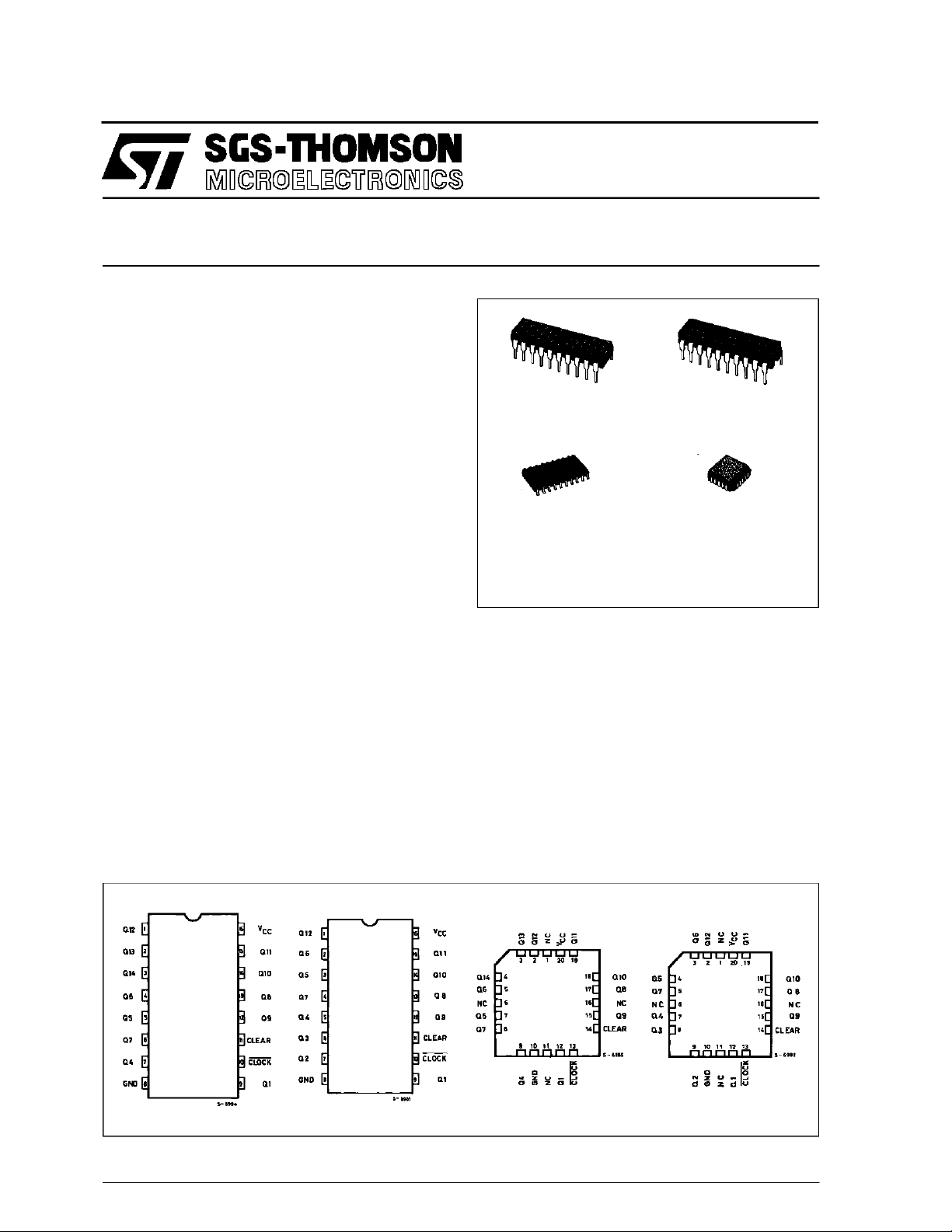
PIN CONNECTION (top view)
HC4 020 HC4 040 HC4020 HC4040
March1993
1/13
Page 2
M54/M74HC4020/4040
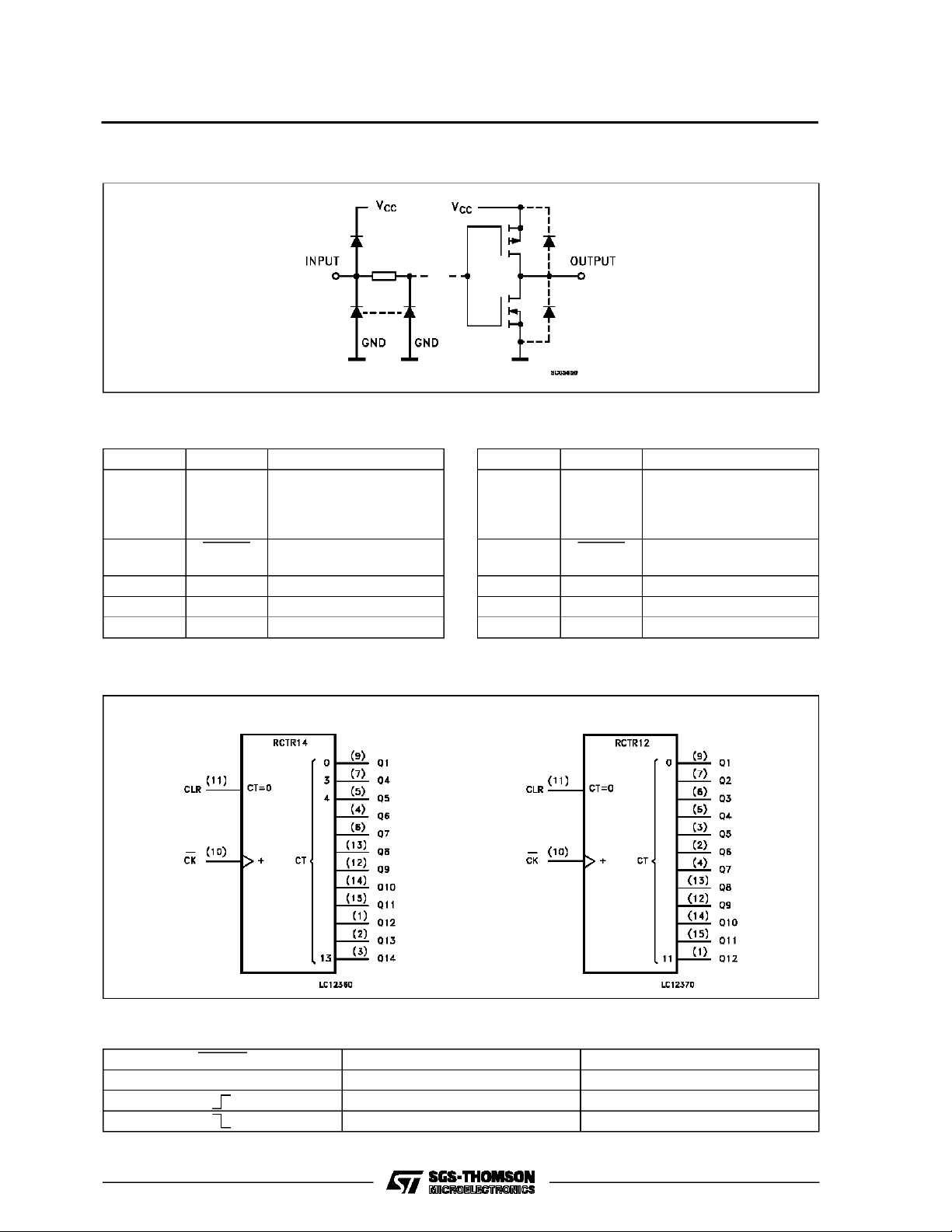
INPUT AND OUTPUT EQUIVALENT CIRCUIT
PIN DESCRIPTION (HC4020)
PIN No SYMBOL NAME AND FUNCTION
9, 7, 6, 5,
3, 2, 4, 13,
12, 14, 15,
1
10 CLOCK Clock Input (LOW to
11 CLEAR Reset Inputs
8 GND Ground (0V)
16 V
Q1, Q4 to
Q14
CC
Parallel Outputs
HIGH, edge triggered)
Positive Supply Voltage
IEC LOGIC SYMBOLS
HC4020 HC404 0
PIN DESCRIPTION (HC 4040)
PIN No SYMBOL NAME AND FUNCTION
9, 7, 6, 5,
3, 2, 4, 13,
12, 14, 15,
1
10 CLOCK Clock Input (LOW to
11 CLEAR Reset Inputs
8 GND Ground (0V)
16 V
Q1 to Q12 Parallel Outputs
HIGH, edge triggered)
CC
Positive Supply Voltage
TRUTH TABLE
CLOCK CLEAR OUTPUT STATE
2/13
X H ALL OUTPUTS = ”L”
L NO CHANGE
L ADVANCE TO NEXT STATE
Page 3
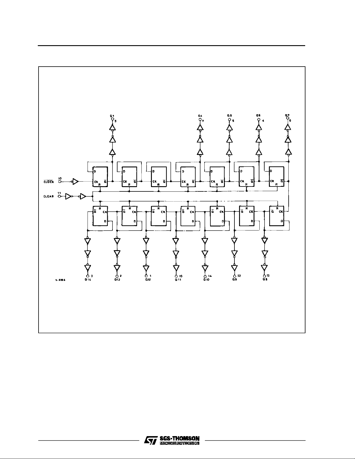
LOGIC DIAGRAM (HC4020)
M54/M74HC4020/4040
3/13
Page 4
M54/M74HC4020/4040
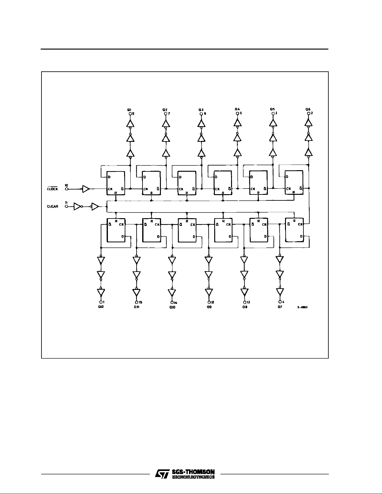
LOGIC DIAGRAM (HC4040)
4/13
Page 5

M54/M74HC4020/4040
ABSOLU TE M AXI MU M R AT INGS
Symbol Parameter Value Unit
V
CC
V
V
O
I
IK
I
OK
I
O
I
or I
CC
P
D
T
stg
T
AbsoluteMaximumRatings arethose valuesbeyond whichdamage tothedevice mayoccur. Functionaloperationunder these conditionisnotimplied.
(*)500 mW:≅ 65oC derate to 300mW by 10mW/oC: 65oCto85oC
RECO MM ENDED OPERAT I N G CO NDITIO NS
Symbol Parameter Value Unit
V
CC
V
I
V
O
T
op
t
r,tf
Supply Voltage -0.5 to +7 V
DC Input Voltage -0.5 to VCC+ 0.5 V
I
DC Output Voltage -0.5 to VCC+ 0.5 V
DC Input Diode Current ± 20 mA
DC Output Diode Current ± 20 mA
DC Output Source Sink Current Per Output Pin ± 25 mA
DC VCCor Ground Current ± 50 mA
GND
Power Dissipation 500 (*) mW
Storage Temperature -65 to +150
Lead Temperature (10 sec) 300
L
Supply Voltage 2 to 6 V
Input Voltage 0 to V
Output Voltage 0 to V
Operating Temperature: M54HC Series
M74HC Series
CC
CC
-55 to +125
-40 to +85
Input Rise and Fall Time VCC= 2 V 0 to 1000 ns
V
= 4.5 V 0 to 500
CC
V
= 6 V 0 to 400
CC
o
C
o
C
V
V
o
C
o
C
5/13
Page 6

M54/M74HC4020/4040
DC SPECIFICATIO NS
Symbol Parameter
V
V
V
V
I
High Level Input
IH
Voltage
Low Level Input
IL
Voltage
High Level
OH
Output Voltage
Low Level Output
OL
Voltage
I
Input Leakage
I
Current
Quiescent Supply
CC
Current
Test Conditions Value
V
(V)
CC
=25oC
A
54HC and 74HC
Min. Typ. Max. Min. Max. Min. Max.
-40 to 85oC
74HC
-55 to 125oC
54HC
Unit
T
2.0 1.5 1.5 1.5
4.5 3.15 3.15 3.15
6.0 4.2 4.2 4.2
2.0 0.5 0.5 0.5
4.5 1.35 1.35 1.35
6.0 1.8 1.8 1.8
2.0
4.5 4.4 4.5 4.4 4.4
6.0 5.9 6.0 5.9 5.9
4.5 I
6.0 I
2.0
4.5 0.0 0.1 0.1 0.1
6.0 0.0 0.1 0.1 0.1
4.5 I
6.0 I
6.0
=
V
I
IO=-20 µA
V
IH
or
V
IL
=-4.0 mA 4.18 4.31 4.13 4.10
O
=-5.2 mA 5.68 5.8 5.63 5.60
O
V
=
I
IO=20µA
V
IH
or
V
IL
= 4.0 mA 0.17 0.26 0.33 0.40
O
= 5.2 mA 0.18 0.26 0.33 0.40
O
VI=VCCor GND ±0.1 ±1 ±1 µA
1.9 2.0 1.9 1.9
0.0 0.1 0.1 0.1
6.0 VI=VCCor GND 4 40 80 µA
V
V
V
V
6/13
Page 7

M54/M74HC4020/4040
AC ELECTRICAL CHARACTERISTICS (CL=50pF,Inputtr=tf=6ns)
Test Conditions Value
T
=25oC
Symbol Parameter
t
t
TLH
THL
Output Transition
Time
V
CC
(V)
2.0 30 75 95 110
4.5 8151922
A
54HC and 74HC
Min. Typ. Max. Min. Max. Min. Max.
6.0 7131619
t
PLH
t
PHL
Propagation
Delay Time
(Qn - Qn+1)
t
t
PLH
PHL
Propagation
Delay Time
(CLOCK Q1)
t
t
PLH
PHL
Propagation
Delay Time
(CLOCK Q1)
t
PHL
Propagation
Delay Time
(CLEAR - Qn)
t
PHL
Propagation
Delay Time
(CLEAR - Qn)
f
MAX
Maximum Clock
Frequency
2.0 20 50 65 75
4.5 5101315
6.0 4 9 11 13
2.0
4.5 21 29 36 44
for HC4020
76 145 180 220
6.0 18 25 31 38
2.0
4.5 17 29 36 44
for HC4040
48 145 180 220
6.0 13 25 31 38
2.0
4.5 18 28 35 42
for HC4020
60 140 175 210
6.0 15 24 30 36
2.0
4.5 18 28 35 42
for HC4040
56 140 175 210
6.0 15 24 30 36
2.0 6.0 15 4.8 4
4.5 30 65 24 20
6.0 35 70 28 24
t
W(H)
t
W(L)
t
W(H)
t
W(H)
t
REM
Minimum Pulse
Width
(CLOCK)
Minimum Pulse
Width
(CLEAR)
Minimum Pulse
Width
(CLEAR)
Minimum
Removal Time
2.0 40 75 95 110
4.5 8151922
6.0 7131619
2.0
4.5 8151922
for HC4020
32 75 95 110
6.0 7131619
2.0
4.5 19 35 44 53
for HC4040
70 175 220 265
6.0 16 30 37 45
2.0
4.5 0 0 0
for HC4020
6.0 0 0 0
t
REM
Minimum
Removal Time
2.0
4.5 5 6 8
for HC4040
6.0 5 5 7
C
C
PD
Input Capacitance 5 10 10 pF
IN
(*) Power Dissipation
34
Capacitance
(*) CPDisdefined as the valueofthe IC’s internal equivalent capacitance which is calculated from the operating current consumption withoutload.
(RefertoTest Circuit).Average operting currentcan be obtained bythe followingequation. ICC(opr) = CPD•VCC•fIN+ICC/2(per FLIP/FLOP)
-40 to 85oC
74HC
-55 to 125oC
54HC
Unit
ns
ns
ns
ns
ns
ns
MHz
ns
ns
ns
000
ns
25 30 40
ns
pF
7/13
Page 8

M54/M74HC4020/4040
SWITCHING CHARACTERISTICS TEST WAVEFORM
TEST CIRCUIT ICC(Opr.)
INPUT WAVEFORMIS THE SAMEAS THAT IN CASE OF SWITCHINGCHARACTERISTICS TEST.
8/13
Page 9

M54/M74HC4020/4040
Plastic DIP16 (0.25) MECHANICAL DATA
DIM.
MIN. TYP. MAX. MIN. TYP. MAX.
a1 0.51 0.020
B 0.77 1.65 0.030 0.065
b 0.5 0.020
b1 0.25 0.010
D 20 0.787
E 8.5 0.335
e 2.54 0.100
e3 17.78 0.700
F 7.1 0.280
I 5.1 0.201
L 3.3 0.130
Z 1.27 0.050
mm inch
P001C
9/13
Page 10

M54/M74HC4020/4040
Ceramic DIP16/1 MECHANICAL DATA
DIM.
MIN. TYP. MAX. MIN. TYP. MAX.
A 20 0.787
B 7 0.276
D 3.3 0.130
E 0.38 0.015
e3 17.78 0.700
F 2.29 2.79 0.090 0.110
G 0.4 0.55 0.016 0.022
H 1.17 1.52 0.046 0.060
L 0.22 0.31 0.009 0.012
M 0.51 1.27 0.020 0.050
N 10.3 0.406
P 7.8 8.05 0.307 0.317
Q 5.08 0.200
mm inch
10/13
P053D
Page 11

SO16 (Narrow) MECHANICAL DATA
M54/M74HC4020/4040
DIM.
MIN. TYP. MAX. MIN. TYP. MAX.
A 1.75 0.068
a1 0.1 0.2 0.004 0.007
a2 1.65 0.064
b 0.35 0.46 0.013 0.018
b1 0.19 0.25 0.007 0.010
C 0.5 0.019
c1 45° (typ.)
D 9.8 10 0.385 0.393
E 5.8 6.2 0.228 0.244
e 1.27 0.050
e3 8.89 0.350
F 3.8 4.0 0.149 0.157
G 4.6 5.3 0.181 0.208
L 0.5 1.27 0.019 0.050
M 0.62 0.024
S8°(max.)
mm inch
P013H
11/13
Page 12

M54/M74HC4020/4040
PLCC20 MECHANICAL DATA
DIM.
MIN. TYP. MAX. MIN. TYP. MAX.
A 9.78 10.03 0.385 0.395
B 8.89 9.04 0.350 0.356
D 4.2 4.57 0.165 0.180
d1 2.54 0.100
d2 0.56 0.022
E 7.37 8.38 0.290 0.330
e 1.27 0.050
e3 5.08 0.200
F 0.38 0.015
G 0.101 0.004
M 1.27 0.050
M1 1.14 0.045
mm inch
12/13
P027A
Page 13

M54/M74HC4020/4040
Information furnished is believed to be accurate and reliable. However, SGS-THOMSON Microelectronics assumes no responsability for the
consequences of use of such information nor for any infringement of patents or other rights of third parties which may results from its use. No
license isgranted by implication orotherwise underany patentor patent rights ofSGS-THOMSON Microelectronics. Specificationsmentioned
in this publication are subject to change without notice. This publication supersedes and replaces all information previously supplied.
SGS-THOMSON Microelectronicsproducts are not authorizedforuse ascritical componentsinlife support devices or systems without express
written approval of SGS-THOMSON Microelectonics.
1994 SGS-THOMSON Microelectronics- All Rights Reserved
Australia - Brazil - France - Germany - Hong Kong - Italy - Japan - Korea - Malaysia - Malta - Morocco - The Netherlands -
Singapore - Spain - Sweden- Switzerland - Taiwan - Thailand - United Kingdom - U.S.A
SGS-THOMSON Microelectronics GROUP OF COMPANIES
13/13
 Loading...