

Page 1
M54/74HC40102
M54/74HC40103
8 STAGE PRE SETTABLE SYNCHR ONOUS DOWN COUNTE RS
.HIGH SPEED
f
= 40 MHz (TYP.) at VCC=5V
MAX
.LOWPOWER DISSIPATION
ICC=4µA(MAX.) at TA=25°C
.HIGH NOISE IMMUNITY
V
NIH=VNIL
.OUTPUT DRIVE CAPABILITY
10 LSTTLLOADS
=28%VCC(MIN.)
B1R
(PlasticPackage)
F1R
(CeramicPackage)
.SYMMETRICAL OUTPUT IMPEDANCE
|IOH|=IOL=4 mA (MIN.)
.BALANCEDPROPAGATION DELAYS
t
PLH=tPHL
.WIDE OPERATINGVOLTAGERANGE
VCC(OPR)= 2 V to 6 V
.PIN AND FUNCTION COMPATIBLE WITH
40102B/40103B
M1R
(MicroPackage)
ORDER CODES :
M54HCXXXXXF1R M74HCXXXXXM1 R
M74HCXXXXXB1R M74HCXXXXX C1R
C1R
(Chip Carrier)
DESCRIPTION
The M54/74HC40102/40103 are highspeedCMOS
8-STAGE PRESETTABLE SYNCHRONOUS
DOWN COUNTERS fabricated with silicon gate
C2MOS technology. They achieve the high speed
operation similar to equivalent LSTTL while maintainingthe CMOS low powerdissipation.
The HC40102,and HC40103 consistof an 8-stage
synchronous down counter with a single output
which is activewhen the internalcountis zero. The
HC40102is configured as two cascaded 4-bit BCD
counters, and the HC40103 contains a single 8-bit
binarycounter. Eachtype hascontrol inputs for enablingordisabling theclock,forclearing thecounter
toitsmaximum count,andforpresettingthecounter
eithersynchronously or asynchronously. All control
inputs and the CARRY-OUT/ZERO-DETECT output are active-low logic. In normal operation, the
counter isdecremented byonecount on eachpositive transition of the CLOCK. Counting is inhibited
when the CARRY-IN/COUNTER ENABLE (CI/CE)
input is high. The CARRY-OUT/ZERO-DETECT
(CO/ZD) output goes low when the count reaches
zero if the CI/CE input is low, and remains low for
one full clock period. When the SYNCHRONOUS
PRESET-ENABLE (SPE) input is low,data at the J
inputis clockedintothe counteron the nextpositive
clocktransition regardless of the state of the CI/CE
input.
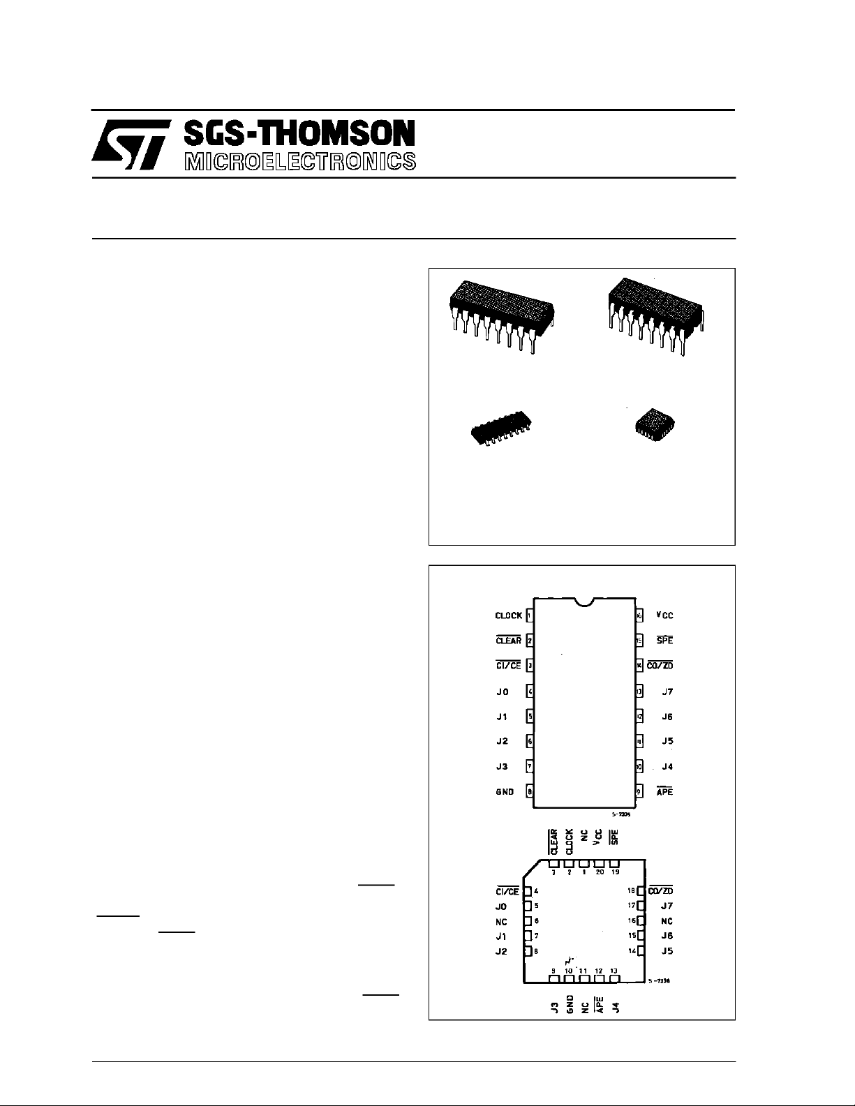
PIN CONNECTIONS (top view)
NC =
No Internal
Connection
March1993
1/14
Page 2
M54/M74HC40102/40103
DESCRIPTION (Continued)
When the ASYNCHRONOUS PRESET-ENABLE
(APE)input islow,data attheJ inputsisasynchronouslyforced into the counter regardless ofthe state
of theSPE, CI/CE, or CLOCK inputs.J Inputs J0-J7
representtwo4-bit BCDwordsfortheHC40102and
a single 8-bit binary word for the HC40103. When
the CLEAR (CLR input is low, the counter is asynchronously cleared to its maximum count (9910for
the HC40102 and 25510for the HC40103 regard-
relationship between control inputis indicated in the
truthtable. Ifall control inputsarehighat thetime of
zero count, the counters will jump to the maximum
count, giving a counting sequence of 100 pr 256
clockpulseslong. The HC40102and HC40103 may
be cascaded usingthe CI/CEinput and the CO/ZD
output, in either a synchronous or ripple mode. All
inputs are equipped with protection circuits against
static discharge and transient excessvoltage.
less of thestateof any other input. The precedence
TRUTH TABLE
CONTROL INPUTS
CLEAR APE SPE CI/CE
H H H H COUNT INHIBIT EVEN IF CLOCK IS GIVEN, NO COUNT IS
H H H L REGULAR COUNT DOWN COUNT AT RISING EDGE OF CLOCK
H H L X SYNCHRONOUS PRESET DATA OF PI TERMINAL IS PRESET AT
H L X X ASYNCRONOUS PRESET DATA PF PI TERMINAL IS
L X X X CLEAR COUNTER IS SET TO MAXIMUM COUNT
X: DON’TCARE - MAXIMUM COUNT:”99” FOR HC40102 AND ”255”: FOR HC40103
MODE FUNCTIONAL DESCRIPTION
MADE
RISING EDGE OF CLOCK
ASYNCHRONOUSLY PRESET TO CLOCK
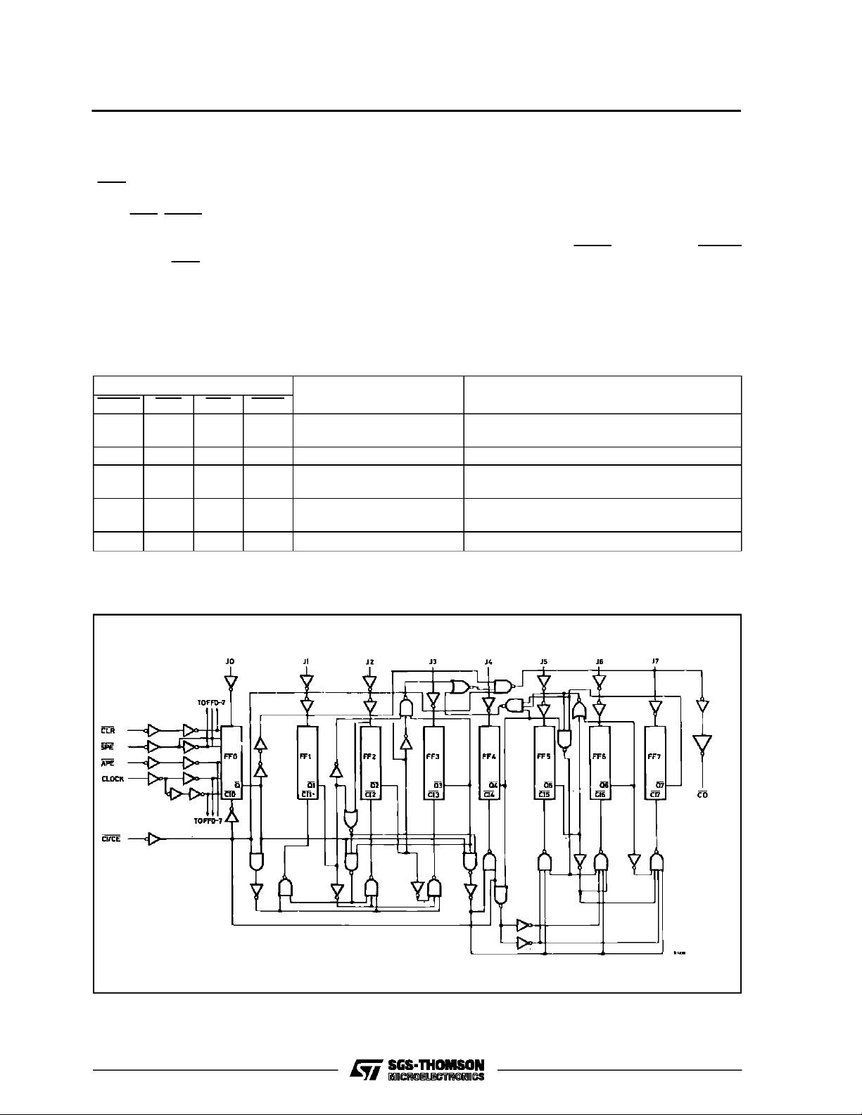
LOGIC DIAGRAM (HC40102)
2/14
Page 3
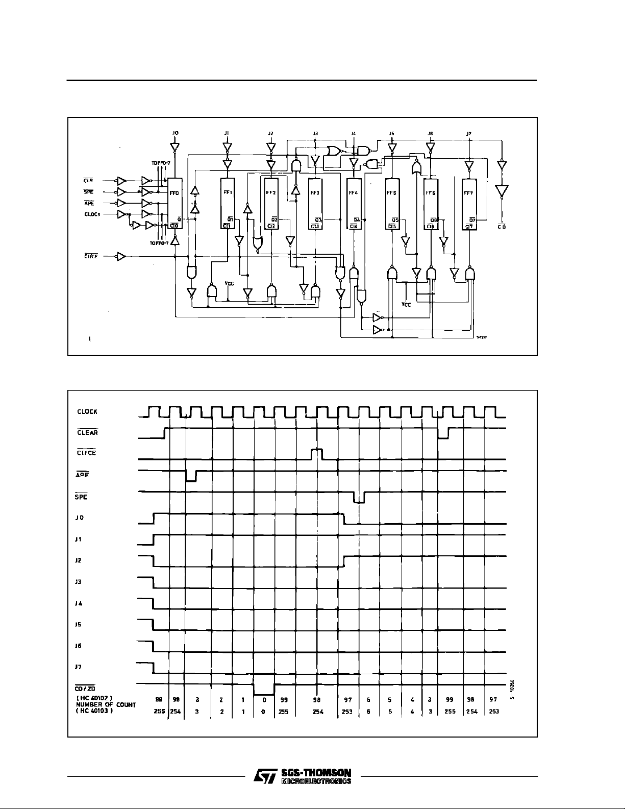
LOGIC DIAGRAM (HC40103)
M54/M74HC40102/40103
TIMING CHART
3/14
Page 4
M54/M74HC40102/40103
PIN No SYMBOL NAME AND FUNCTION
1 CLOCK CLock Input (LOW to
HIGH edge triggered)
2 CLEAR Asynchronous Master
Reset Input (Active LOW)
3 CI/CE Terminal Enable Input
4, 5, 6, 7, 10,
11, 12, 13
9 APE Asynchronous Preset
14 CO/ZD Terminal Count Output
15 SPE Synchronous Preset
8 GND Ground (0V)
16 V
IEC LOGIC SYMBOLS
J0 to J9 Jam Inputs
Enable Input (Active LOW)
(Active LOW)
Enable Input (Active LOW)
CC
Positive Supply Voltage
HC4 0102 HC401 03
INPUT AND OUTPUT EQUIVALENT CIRCUITPIN DESCRIPTION
ABSOLU TE M AXI MUM R AT I NG S
Symbol Parameter Value Unit
V
CC
V
V
O
I
IK
I
OK
I
O
I
or I
CC
P
D
T
stg
T
AbsoluteMaximumRatingsarethosevalues beyondwhichdamage tothedevicemayoccur.Functionaloperationunder thesecondition isnotimplied.
(*)500 mW:≅ 65oC derate to 300 mWby 10mW/oC: 65oCto85oC
4/14
Supply Voltage -0.5 to +7 V
DC Input Voltage -0.5 to VCC+ 0.5 V
I
DC Output Voltage -0.5 to VCC+ 0.5 V
DC Input Diode Current ± 20 mA
DC Output Diode Current ± 20 mA
DC Output Source Sink Current Per Output Pin ± 25 mA
DC VCCor Ground Current ± 50 mA
GND
Power Dissipation 500 (*) mW
Storage Temperature -65 to +150
Lead Temperature (10 sec) 300
L
o
C
o
C
Page 5
M54/M74HC40102/40103
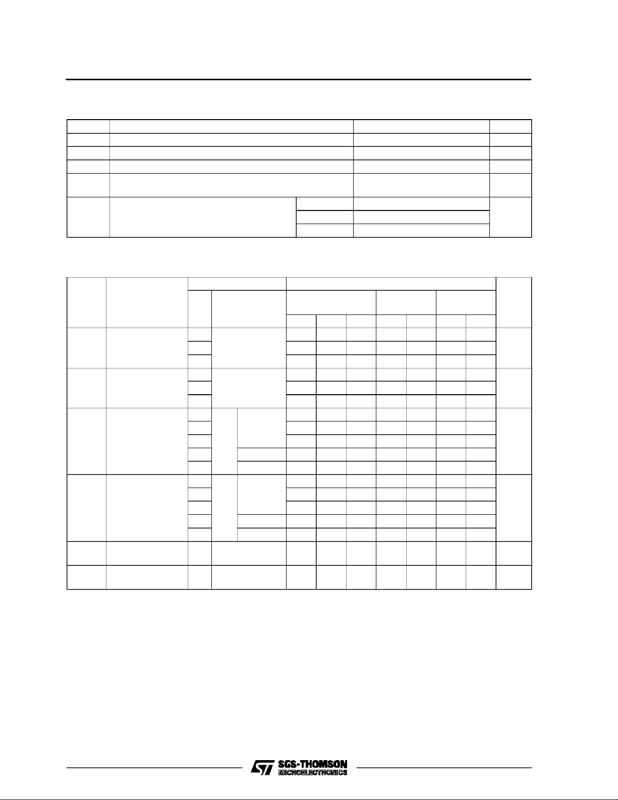
RECO MM ENDED OPERAT IN G CO NDITIO NS
Symbol Parameter Value Unit
V
V
V
T
t
r,tf
DC SPECIFICATIONS
Symbol Parameter
V
IH
V
V
OH
V
OL
I
I
CC
Supply Voltage 2 to 6 V
CC
Input Voltage 0 to V
I
Output Voltage 0 to V
O
Operating Temperature: M54HC Series
op
M74HC Series
CC
CC
-55 to +125
-40 to +85
Input Rise and Fall Time VCC= 2 V 0 to 1000 ns
V
= 4.5 V 0 to 500
CC
V
= 6 V 0 to 400
CC
Test Conditions Value
V
(V)
CC
=25oC
T
A
54HC and 74HC
-40 to 85oC
74HC
-55 to 125oC
Min. Typ. Max. Min. Max. Min. Max.
High Level Input
Voltage
2.0 1.5 1.5 1.5
4.5 3.15 3.15 3.15
6.0 4.2 4.2 4.2
Low Level Input
IL
Voltage
2.0 0.5 0.5 0.5
4.5 1.35 1.35 1.35
6.0 1.8 1.8 1.8
High Level
Output Voltage
Low Level Output
Voltage
Input Leakage
I
Current
Quiescent Supply
2.0
V
=
I
4.5 4.4 4.5 4.4 4.4
6.0 5.9 6.0 5.9 5.9
4.5 I
6.0 I
2.0
4.5 0.0 0.1 0.1 0.1
6.0 0.0 0.1 0.1 0.1
4.5 I
6.0 I
6.0
IO=-20 µA
V
IH
or
V
IL
=-4.0 mA 4.18 4.31 4.13 4.10
O
=-5.2 mA 5.68 5.8 5.63 5.60
O
V
=
I
IO=20µA
V
IH
or
V
IL
= 4.0 mA 0.17 0.26 0.33 0.40
O
= 5.2 mA 0.18 0.26 0.33 0.40
O
VI=VCCor GND ±0.1 ±1 ±1 µA
1.9 2.0 1.9 1.9
0.0 0.1 0.1 0.1
6.0 VI=VCCor GND 4 40 80 µA
Current
54HC
V
V
o
C
o
C
Unit
V
V
V
V
5/14
Page 6

M54/M74HC40102/40103
AC ELECTRICAL CHARACTERISTICS (CL=50pF,Inputtr=tf=6ns)
Test Conditions Value
T
=25oC
Symbol Parameter
t
t
TLH
THL
Output Transition
Time
V
CC
(V)
2.0 30 75 95 110
4.5 8151922
A
54HC and 74HC
Min. Typ. Max. Min. Max. Min. Max.
6.0 7131619
t
PLH
t
PHL
Propagation
Delay Time
(CK - CO/ZD)
t
t
PLH
PHL
Propagation
Delay Time
(APE- CO/ZD)
t
t
PLH
PHL
Propagation
Delay Time
(CL -CO/ZD)
t
t
PLH
PHL
Propagation
Delay Time
(CI/CE - CO/ZD)
f
MAX
Propagation
Delay Time
2.0 96 185 230 280
4.5 24 37 46 56
6.0 20 31 39 47
2.0 116 225 280 340
4.5 29 45 56 68
6.0 25 38 48 57
2.0 104 200 250 300
4.5 26 40 50 60
6.0 22 34 43 51
2.0 48 95 120 145
4.5 12 19 24 29
6.0 10 16 20 24
2.0 4 8 3 2.6
4.5 20 32 16 13
6.0 24 38 19 15
C
C
PD
Input Capacitance 5 10 10 10 pF
IN
(*) Power Dissipation
60
Capacitance
(*) CPDisdefined as the valueof the IC’sinternal equivalent capacitance which is calculated from the operatingcurrent consumption withoutload.
(RefertoTest Circuit).Average opertingcurrentcan be obtained bythe followingequation. ICC(opr) = CPD•VCC•fIN+I
-40 to 85oC
74HC
-55 to 125oC
54HC
CC
Unit
ns
ns
ns
ns
ns
pF
pF
TEST CIRCUIT ICC(Opr.)
INPUT TRANSITIONTIME ISTHE SAME AS THAT INCASE OF SWITCHINGCHARACTERISTICSTEST.
6/14
Page 7

FUNCTIONAL DESCRIPTION
The HC40102 and HC40103 are 8-stage presettable synchronous down counters. Carry Out/Zero
Detect (CO/ZD) is output at the ”L” level for the
periodof 1 bit when the readoutbecomes ”0”. The
HC40102 adopts binary coded decimal notation,
making setting up to 99 counts possible. While the
HC40103adopts8-bitbinary counterand canset up
to 255counts.
COUNT OPERATION
At the”H” level of controlinputof CLEAR, SPE and
APE,the counter carriersoutdown count operation
onebyoneattheriseofpulsegiventoCLOCKinput.
Count operation can be inhibited by setting Carry
Input/Clock Enable CI/CEto the”H” level.
CO/ZD is output at the ”L” level when the readout
becomes ”0” but is not output even if the readout
becomes ”0” when CI/CE is at the ”H” level, thus
maintaining the”H” level.
Synchronous cascade operation can be carried out
by using CI/CEinput and CO/ZD output.
M54/M74HC40102/40103
The contents of countjump to maximum count (99
for the HC40102 and 225 for theHC40103) if clock
is given when the readout is ”0”. Therefore, operation of100-frequency division and that of 256-frequencydivisionare carriedoutfortheHC40102and
HC40103, respectively, when clock input alone is
givenwithout variouskinds of preset operation.
PRESETOPERATIONAND RESET OPERATION
WhenClear(CLEAR) inputis settothe”L” level,the
readout is set to the maximum count independetly
of other inputs. When Asynchronous PresetEnable
(APE)input isset to the”L” level,readouts givenon
J0toJ7can be presetasynchronously tocounterindependently of inputs other than CLEAR input.
When Synchronous Preset Enable (SPE) is set to
the ”L” level,the readouts givenon J0to J7 can be
preset to counter synchronously with the rise of
clock.
Astotheseoperation modes,referto the truthtable.
Input Output
CLEAR APE SPE J T E CLO CK Qn+1
LXXXXX L
HLXLXX L
HLXHXX H
HHLLX
HHLHX
HHLXX
HHHXL
HHHXHX
_
▲
_L
_
▲
_H
_
▼
_
_
▲
_Qn
__
Q
__
Q
n
n
7/14
Page 8

M54/M74HC40102/40103
SWITCHING CHARACTERISTICS TEST WAVEFORM
WAVEFORM 1 WAVEFORM 2
WAVEFORM 3 WAVEFORM 4
WAVEFORM 5 WAVEFORM 6
(**F/F outputis internal signal of IC)
8/14
Page 9

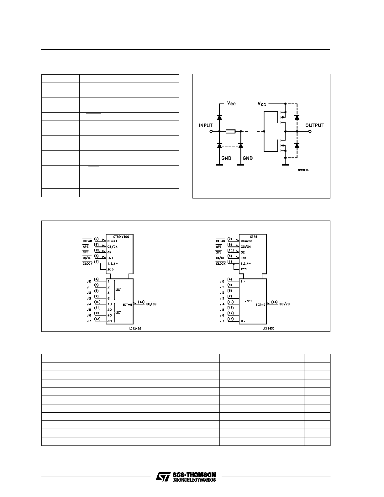
EXAMPLE OF TYPICAL APPLICATION
M54/M74HC40102/40103
PROGRAMMABLE DIVIDE-BY-N COUNTER
PARALLEL CARRY CASCADING
f
• f
•Timingchartwhen N = ”3”
• HC40102... 1/2to1/100are dividable
• HC40103... 1/2to1/256are dividable
IN
=
OUT
N
+ 1
(J0, J1 = VCC, J2– J7 = GND)
*Atsynchronous cascade connection, huzzerd occurs atC0 outputafteritssecondstagewhen digitplacechanges, duetodelayarrival.Therefore,
takegatefromHC32or the like,notfromC0output at the rearstagedirectly.
PROGRAMMABLE TIMER
Note :The above formula does not take into account the phase of clock input. Therefore, the real pulse width is the distance between the
above formula-1/fIN ∼ the above formula.
9/14
Page 10

M54/M74HC40102/40103
Plastic DIP16 (0.25) MECHANICAL DATA
DIM.
MIN. TYP. MAX. MIN. TYP. MAX.
a1 0.51 0.020
B 0.77 1.65 0.030 0.065
b 0.5 0.020
b1 0.25 0.010
D 20 0.787
E 8.5 0.335
e 2.54 0.100
e3 17.78 0.700
F 7.1 0.280
I 5.1 0.201
L 3.3 0.130
Z 1.27 0.050
mm inch
10/14
P001C
Page 11

M54/M74HC40102/40103
Ceramic DIP16/1 MECHANICAL DATA
DIM.
MIN. TYP. MAX. MIN. TYP. MAX.
A 20 0.787
B 7 0.276
D 3.3 0.130
E 0.38 0.015
e3 17.78 0.700
F 2.29 2.79 0.090 0.110
G 0.4 0.55 0.016 0.022
H 1.17 1.52 0.046 0.060
L 0.22 0.31 0.009 0.012
M 0.51 1.27 0.020 0.050
N 10.3 0.406
P 7.8 8.05 0.307 0.317
Q 5.08 0.200
mm inch
P053D
11/14
Page 12

M54/M74HC40102/40103
SO16 (Narrow) MECHANICAL DATA
DIM.
MIN. TYP. MAX. MIN. TYP. MAX.
A 1.75 0.068
a1 0.1 0.2 0.004 0.007
a2 1.65 0.064
b 0.35 0.46 0.013 0.018
b1 0.19 0.25 0.007 0.010
C 0.5 0.019
c1 45° (typ.)
D 9.8 10 0.385 0.393
E 5.8 6.2 0.228 0.244
e 1.27 0.050
e3 8.89 0.350
F 3.8 4.0 0.149 0.157
G 4.6 5.3 0.181 0.208
L 0.5 1.27 0.019 0.050
M 0.62 0.024
S8°(max.)
mm inch
12/14
P013H
Page 13

PLCC20 MECHANICAL DATA
M54/M74HC40102/40103
DIM.
MIN. TYP. MAX. MIN. TYP. MAX.
A 9.78 10.03 0.385 0.395
B 8.89 9.04 0.350 0.356
D 4.2 4.57 0.165 0.180
d1 2.54 0.100
d2 0.56 0.022
E 7.37 8.38 0.290 0.330
e 1.27 0.050
e3 5.08 0.200
F 0.38 0.015
G 0.101 0.004
M 1.27 0.050
M1 1.14 0.045
mm inch
P027A
13/14
Page 14

M54/M74HC40102/40103
Information furnished is believed to be accurate and reliable. However, SGS-THOMSON Microelectronicsassumes no responsability for the
consequences of use of such information nor for any infringement of patents or other rightsof thirdparties which mayresults from itsuse. No
license isgranted by implication orotherwise underany patentor patentrights of SGS-THOMSON Microelectronics. Specificationsmentioned
in this publication are subject to changewithout notice.This publication supersedes and replaces all information previouslysupplied.
SGS-THOMSON Microelectronicsproducts are notauthorizedforuse ascritical componentsinlife support devicesor systemswithout express
written approval of SGS-THOMSON Microelectonics.
1994 SGS-THOMSON Microelectronics- All RightsReserved
Australia - Brazil - France- Germany- HongKong - Italy - Japan- Korea - Malaysia - Malta - Morocco- The Netherlands-
Singapore - Spain - Sweden- Switzerland -Taiwan - Thailand - UnitedKingdom - U.S.A
SGS-THOMSON Microelectronics GROUP OF COMPANIES
14/14
 Loading...