

Page 1
M74HC374
OCTAL D-TYPE FLIP FLOP
WITH 3 STATE OUTPUT NON INVERTING
■ HIGH SPEED:
f
= 90MHz (TYP.) at VCC = 6V
MAX
■ LOW POWER DISSIPATION:
I
= 4µA(MAX.) at TA=25°C
CC
■ HIGH NOISE IMMUNITY:
V
= V
NIH
■ SYMMETRICAL OUTPUT IMPEDANCE:
|I
| = IOL = 6mA (MIN)
OH
■ BALANCED PROPAGATION DELAYS:
t
≅ t
PLH
■ WIDE OPERATING VOLTAGE RANGE:
V
(OPR) = 2V to 6V
CC
■ PIN AND FUNCTION COMPATIBLE WITH
= 28 % VCC (MIN.)
NIL
PHL
74 SERIES 374
DESCRIPTION
The M74HC374 is an high speed CMOS OCTAL
D-TYPE FLIP FLOP WITH 3-STATE OUTPUTS
NON INVERTING fabricated with sub-micron
silicon gate C
2
MOS technology.
This 8 bit D-TYPE FLIP FLOP is con trolled by a
clock input (CK) and an o utpu t enable input (OE
On the positive transition of the clock, the Q
outputs will be set to the logic state that were
setup at the D inputs.
While the OE
input is at low level, the eight outputs
will be in a norm al logic state (high or low logic
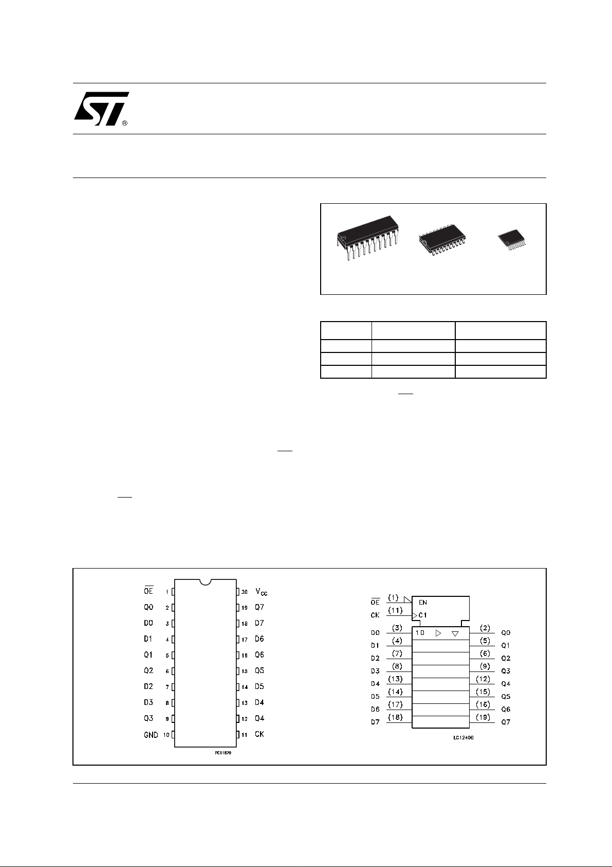
ORDER CODES
PACKAGE TUBE T & R
DIP M74HC374B1R
SOP M74HC374M1R M74HC374RM13TR
TSSOP M74HC374TTR
level) and while OE
is high the outputs will be in
a high impedance state.
The output control does not affect the internal
operation of flip-flops; that is, the old data can be
retained or the new data can be entered even
).
while the outputs are off.
All inputs are equipped with protection circuits
against static discharge and transient excess
voltage.
TSSOPDIP SOP
PIN CONNECTION AND IEC LOGIC SYMBOLS
1/11July 2001
Page 2
M74HC374
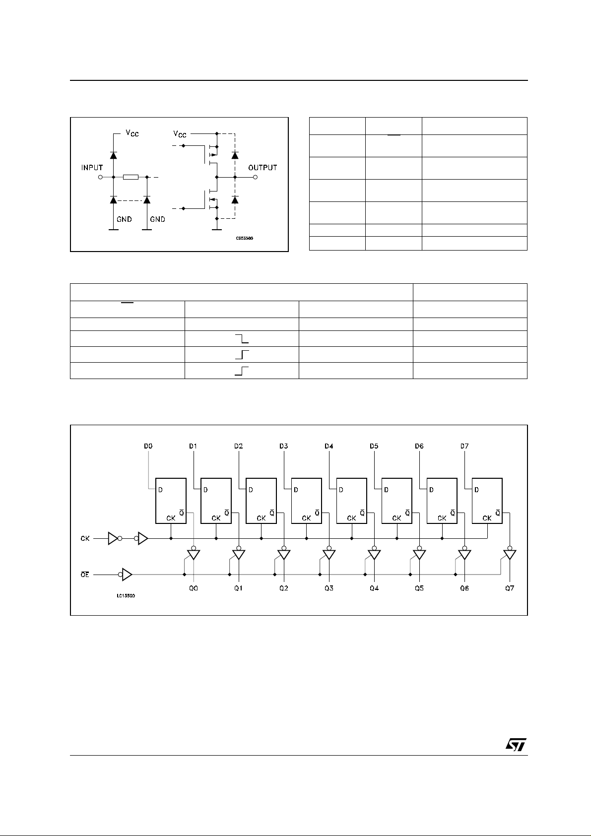
INPUT AND OUTPUT EQUIVALENT CIRCUIT PIN DESCRIPTION
PIN No SYMBOL NAME AND FUNCTION
1OE
2, 5, 6, 9, 12,
15, 16, 19
3, 4, 7, 8, 13,
14, 17, 18
11 CK Clock Input (LOW to
10 GND Ground (0V)
20 V
TRUTH TABLE
INPUTS OUTPUT
Q0 to Q7 3 State Outputs
D0 to D7 Data Inputs
CC
3 State Output Enable
Input (Active LOW)
HIGH, edge triggered)
Positive Supply Voltage
OE
HXXZ
L X NO CHANGE
LLL
LHH
X: Don’t Care
Z: High Impedance
LOGIC DIAGRAM
CK D Q
This log i c diagram has not be used to est i m at e propagation delays
2/11
Page 3
M74HC374
ABSOLUTE MAXIMUM RATINGS
Symbol Parameter Value Unit
V
V
V
I
I
OK
I
I
or I
CC
P
T
T
Absolute Maximum Ratings are those values beyond which damage to the device may occur. Functional operation under these conditions is
not implied
(*) 500mW at 65
RECOMMENDED OPERATING CONDITIONS
Symbol Parameter Value Unit
V
V
V
T
t
r
Supply Voltage
CC
DC Input Voltage -0.5 to VCC + 0.5
I
DC Output Voltage -0.5 to VCC + 0.5
O
DC Input Diode Current
IK
DC Output Diode Current
DC Output Current
O
DC VCC or Ground Current
GND
Power Dissipation
D
Storage Temperature
stg
Lead Temperature (10 sec)
L
°C; derate to 300mW by 10mW/°C from 65°C to 85°C
Supply Voltage
CC
Input Voltage 0 to V
I
Output Voltage 0 to V
O
Operating Temperature
op
Input Rise and Fall Time VCC = 2.0V
, t
f
V
V
CC
CC
= 4.5V
= 6.0V
-0.5 to +7 V
± 20 mA
± 20 mA
± 35 mA
± 70 mA
500(*) mW
-65 to +150 °C
300 °C
2 to 6 V
CC
CC
-55 to 125 °C
0 to 1000 ns
0 to 500 ns
0 to 400 ns
V
V
V
V
3/11
Page 4
M74HC374
DC SPECIFICATIONS
Symbol Parameter
V
V
V
V
I
I
High Level Input
IH
Voltage
Low Level Input
IL
Voltage
High Level Output
OH
Voltage
Low Level Output
OL
Voltage
I
Input Leakage
I
Current
High Impedance
OZ
Output Leakage
Current
Quiescent Supply
CC
Current
Test Condition Value
V
(V)
CC
= 25°C
A
Min. Typ. Max. Min. Max. Min. Max.
-40 to 85°C -55 to 125°C
T
2.0 1.5 1.5 1.5
6.0 4.2 4.2 4.2
2.0 0.5 0.5 0.5
6.0 1.8 1.8 1.8
2.0
4.5
6.0
4.5
6.0
2.0
4.5
6.0
4.5
6.0
6.0
6.0
6.0
IO=-20 µA
I
=-20 µA
O
I
=-20 µA
O
I
=-6.0 mA
O
I
=-7.8 mA
O
IO=20 µA
I
=20 µA
O
I
=20 µA
O
I
=6.0 mA
O
I
=7.8 mA
O
= VCC or GND
V
I
= VIH or V
V
I
IL
VO = VCC or GND
= VCC or GND
V
I
1.9 2.0 1.9 1.9
4.4 4.5 4.4 4.4
5.9 6.0 5.9 5.9
4.18 4.31 4.13 4.10
5.68 5.8 5.63 5.60
0.0 0.1 0.1 0.1
0.0 0.1 0.1 0.1
0.0 0.1 0.1 0.1
0.17 0.26 0.33 0.40
0.18 0.26 0.33 0.40
± 0.1 ± 1 ± 1 µA
± 0.5 ± 5 ± 10 µA
44080µA
Unit
V4.5 3.15 3.15 3.15
V4.5 1.35 1.35 1.35
V
V
4/11
Page 5
AC ELECTRICAL CHARACTERISTICS (CL = 50 pF, Input tr = tf = 6ns)
Test Condition Value
T
Symbol Parameter
t
TLH tTHL
t
PLH tPHL
Output Transition
Time
Propagation Delay
Time
(CLOCK - Q)
t
PZL tPZH
High Impedance
Output Enable
Time
t
PLZ tPHZ
High Impedance
Output Disable
Time
f
MAX
t
W(L)
t
W(H)
Maximum Clock
Frequency
Minimum Pulse
Width (CLOCK)
Minimum Set-up
t
s
Time
Minimum Hold
t
h
Time
C
V
CC
(V)
L
(pF)
2.0
50
6.0 6101315
2.0
50
6.0 13 24 30 36
2.0
150
6.0 17 32 41 48
2.0
R
50
= 1 KΩ
L
6.0 11 23 29 35
2.0
150
L
= 1 KΩ
R
6.0 15 31 39 48
2.0
R
50
= 1 KΩ
L
6.0 13 21 26 32
2.0
50
6.0 37 90 30 25
2.0
50
6.0 6131619
2.0
50
6.0 4131619
2.0
50
6.0 0 0 0
= 25°C
A
Min. Typ. Max. Min. Max. Min. Max.
25 60 75 90
45 140 175 210
60 190 240 285
39 135 170 205
54 185 230 280
30 125 155 190
6.2 18 5 4.2
15 75 95 110
25 75 95 110
000
M74HC374
-40 to 85°C -55 to 125°C
Unit
ns4.5 7121518
ns4.5 15 28 35 42
ns4.5 20 38 48 57
ns4.5 13 27 34 41
ns4.5 18 37 46 56
ns4.5 14 25 31 38
MHz4.5 31 75 25 21
ns4.5 6151922
ns4.5 6151922
ns4.5 0 0 0
CAPACITIVE CHARACTERISTICS
Test Condition Value
= 25°C
Symbol Parameter
C
C
C
Input Capacitance
IN
Output
OUT
Capacitance
Power Dissipation
PD
Capacitance (note
V
CC
(V)
T
A
Min. Typ. Max. Min. Max. Min. Max.
5101010pF
10 pF
47 pF
1)
1) CPD is defined as the value of the IC’s internal equivalent capacitance which is calculated from the operating current consumption without
load. (Refer to Test Circuit). Average operating current can be obtained by the following equation. I
Flop) and the C
when n pcs of F lip Flop opera te, can be gained by the following equation: C
PD
-40 to 85°C -55 to 125°C
= CPD x VCC x fIN + ICC/8 (per Flip
CC(opr)
PD(TOTAL)
= 30 + 17 x n (pF)
Unit
5/11
Page 6

M74HC374
TEST CIRCUIT
TEST SWITCH
t
, t
PLH
PHL
, t
t
PZL
PLZ
t
, t
PZH
PHZ
CL = 50pF/150pF or equivalent (includes jig and probe capacitance)
= 1KΩ or equivalent
R
1
R
= Z
of pulse generator (typically 50Ω)
T
OUT
Open
V
CC
GND
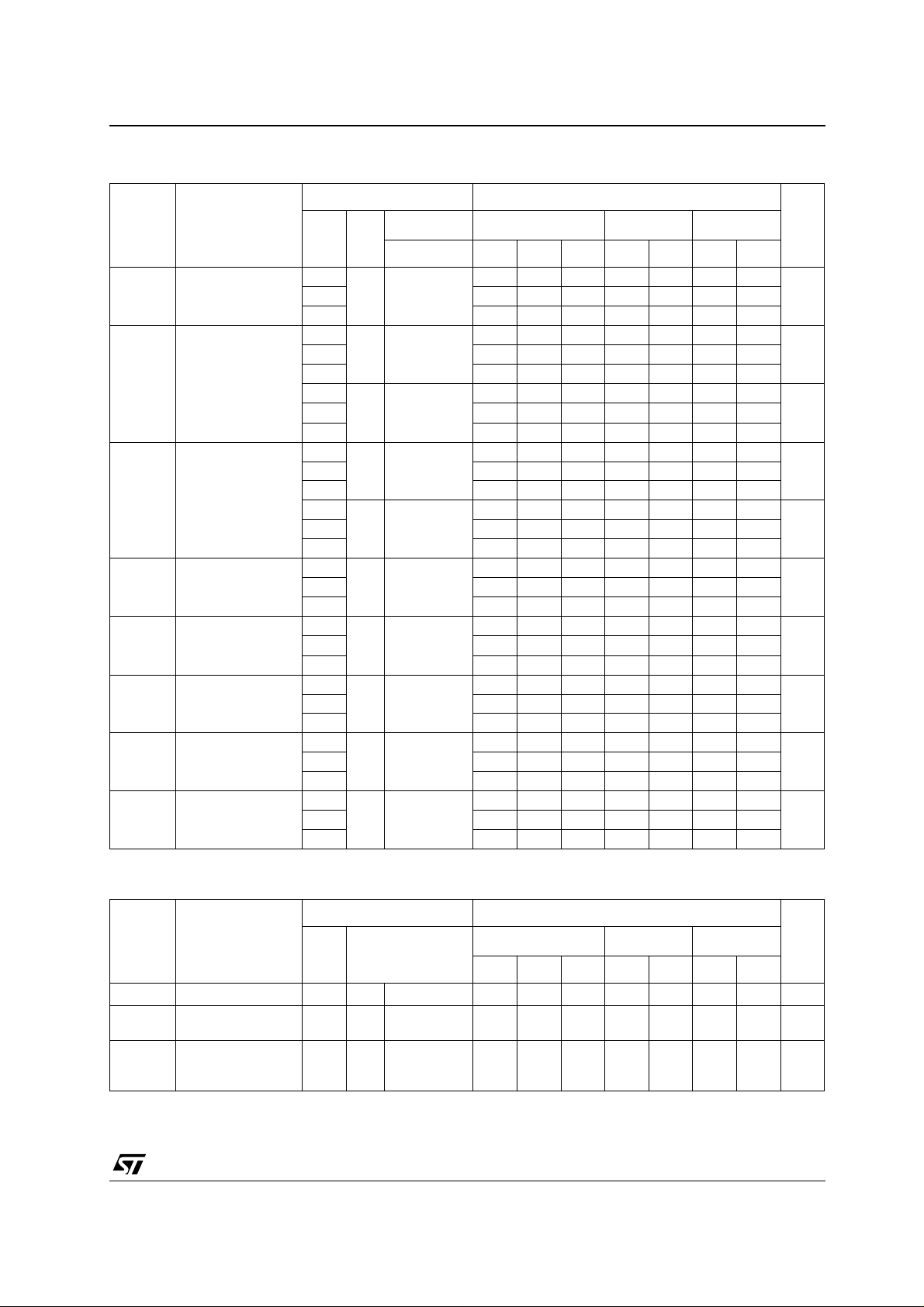
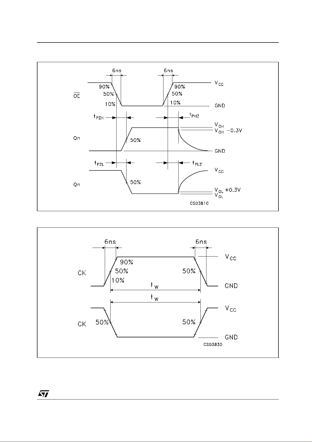
WAVEFORM 1: CK TO Qn PROPAGATION DELAYS, CK FMAX, Dn TO CK SETUP AND HOLD
TIMES (f=1MHz; 50% duty cycle)
6/11
Page 7
WAVEFORM 2: OUTPUT ENABLE AND DISABLE TIMES (f=1MHz; 50% duty cycl e )
M74HC374
WAVEFORM 3: MINIMUM PULSE WIDTH (CK) (f=1MHz; 50% duty cycle)
7/11
Page 8

M74HC374
Plastic DIP-20 (0.25) MECHANICAL DATA
mm. inch
DIM.
MIN. TYP MAX. MIN. TYP. MAX.
a1 0.254 0.010
B 1.39 1.65 0.055 0.065
b 0.45 0.018
b1 0.25 0.010
D 25.4 1.000
E 8.5 0.335
e 2.54 0.100
e3 22.86 0.900
F 7.1 0.280
I 3.93 0.155
L 3.3 0.130
Z 1.34 0.053
8/11
P001J
Page 9

SO-20 MECHANICAL DATA
M74HC374
DIM.
MIN. TYP MAX. MIN. TYP. MAX.
A 2.65 0.104
a1 0.1 0.2 0.004 0.008
a2 2.45 0.096
b 0.35 0.49 0.014 0.019
b1 0.23 0.32 0.009 0.012
C 0.5 0.020
c1 45° (typ.)
D 12.60 13.00 0.496 0.512
E 10.00 10.65 0.393 0.419
e 1.27 0.050
e3 11.43 0.450
F 7.40 7.60 0.291 0.300
L 0.50 1.27 0.020 0.050
M 0.75 0.029
S8° (max.)
mm. inch
PO13L
9/11
Page 10

M74HC374
TSSOP20 MECHANICAL DATA
mm. inch
DIM.
MIN. TYP MAX. MIN. TYP. MAX.
A 1.2 0.047
A1 0.05 0.15 0.002 0.004 0.006
A2 0.8 1 1.05 0.031 0.039 0.041
b 0.19 0.30 0.007 0.012
c 0.09 0.20 0.004 0.0089
D 6.4 6.5 6.6 0.252 0.256 0.260
E 6.2 6.4 6.6 0.244 0.252 0.260
E1 4.3 4.4 4.48 0.169 0.173 0.176
e 0.65 BSC 0.0256 BSC
K0° 8°0° 8°
L 0.45 0.60 0.75 0.018 0.024 0.030
A2
A
A1
b
e
K
c
L
E
D
E1
PIN 1 IDENTIFICATION
10/11
1
0087225C
Page 11

M74HC374
Information furnished is bel ieved to be accurate and reliable. However, STMicroe lectronics assumes no responsibility for the
consequences of use of such information nor for any infringement of patents or other rights of third parties which may result from
its use. No li cense is granted by imp lication or otherwise under a ny patent or patent rig hts of STMicroelectronics. Spec ific at ions
mentioned in this publication ar e subject to change without notice. This publication supersedes and replaces all information
previously supplied. S TMicroelectronics products are not authorized for use as critica l components in life suppo rt devices or
systems without express written approval of STMicroelectronics.
Australi a - Brazil - Chi na - Finland - F rance - Germany - Hong Kon g - I ndia - Italy - Japan - Malay sia - Malta - Morocco
© The ST logo is a registered trademark of STMicroelectronics
© 2000 STM icroelectronics - Printed in Ital y - All Rights Reserved
STMicr o el ectronics GROUP OF COMPANIES
Singapo re - Spain - Sweden - Switzerland - Uni ted Kingdom
© http://www.st.com
11/11
 Loading...