

Page 1
OCTAL D-TYPE LATCH WITH 3 STATE OUTPUT
HC373 NON INVERTING - HC533 INVERTING
.HIGH SPEED
tPD= 11 ns(TYP.) AT VCC=5V
.LOWPOWERDISSIPATION
ICC=4µA(MAX.) AT TA=25°C
.HIGH NOISEIMMUNITY
V
NIH=VNIL
=28%VCC(MIN.)
.OUTPUT DRIVE CAPABILITY
15 LSTTL LOADS
.SYMMETRICALOUTPUT IMPEDANCE
IOL=IOH= 6 mA (MIN.)
.BALANCEDPROPAGATION DELAYS
t
PLH=tPHL
.WIDE OPERATINGVOLTAGE RANGE
VCC(OPR)= 2V TO6 V
.PIN ANDFUNCTION COMPATIBLE
WITH 54/74LS373/533
DESCRIPTION
The M54/74HC373/533 are high speed CMOS
OCTAL LATCH WITH 3-STATE OUTPUTS
fabricated within silicon gateC2MOS technology.
These ICs achive the high speed operation similar
to equivalent LSTTL while maintaning the CMOS
low power dissipation.
These8bit D-Type latches are controlled bya latch
enable input (LE) and aoutput enable input (OE).
While the LE input is held at a high level, the Q
outputs will follow the data input precisely or
inversely. When the LE is taken low, theQ outputs
willbelatchedpreciselyorinversely atthelogiclevel
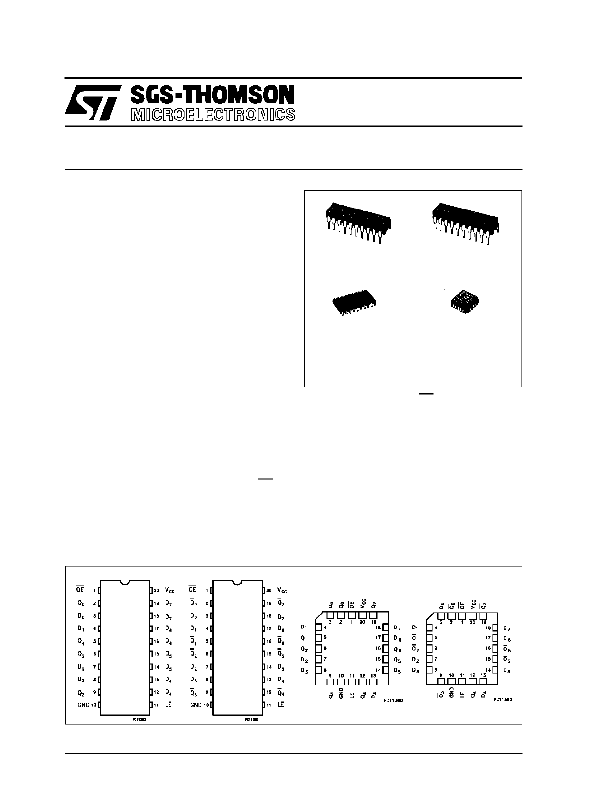
M54/74HC373
M54/ 74 HC5 33
B1R
(PlasticPackage)
M1R
(MicroPackage)
ORDER CODE S :
M54HC XXXF1R M74HC XXXM1R
M74HC XXXB1R M74H CXXXC1R
of D input data. While the OE input is at low level,
the eightoutputs willbe in anormal logic state(high
or lowlogiclevel) andwhile high levelthe outpts will
be in a high impedance state.
The application designer has a choise of
combination of inverting andnon invertingoutputs.
The three state output configuration and the wide
choise of outline make bus organized system
simple.
All inputs are equipped with protection circuits
against discharge andtransient excessvoltage.
F1R
(CeramicPackage)
C1R
(Chip Carrier)
PIN CONNECTION (top view)
HC373 HC533 HC373 HC533
October 1993
1/13
Page 2
M54/M74HC373/533
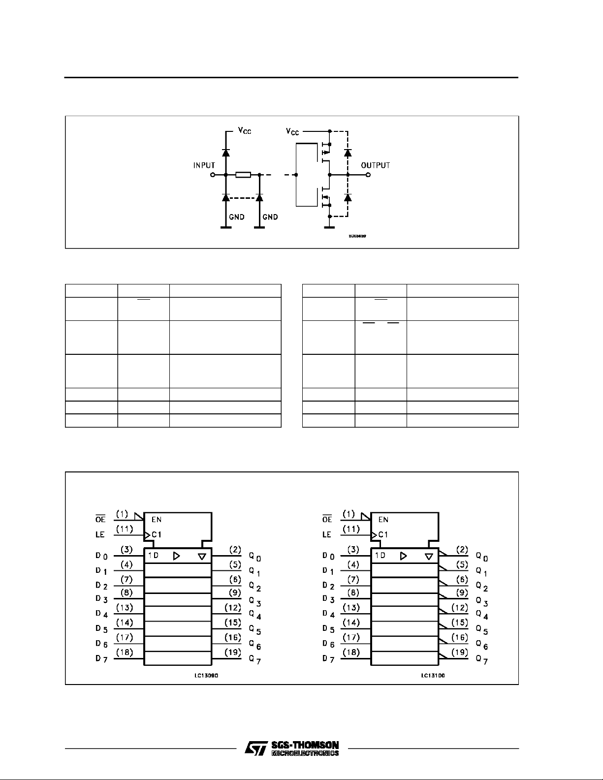
INPUT AND OUTPUT EQUIVALENT CIRCUIT
PIN DESC RIPTION (H C373)
PIN No SYMBOL NAME AND FUNCTION
1 OE 3 State output Enable
Input (Active LOW)
2, 5, 6, 9,
12, 15, 16,
19
3, 4, 7, 8,
13, 14, 17,
18
11 LE Latch Enable Input
10 GND Ground (0V)
20 V
Q0 to Q7 3 State outputs
D0 to D7 Data Inputs
CC
Positive Supply Voltage
IEC LOGIC SYMBOLS
HC373 HC533
PIN DESCRIPTION (HC533)
PIN No SYMBOL NAME AND FUNCTION
1 OE 3 State output Enable
Input (Active LOW)
2, 5, 6, 9,
12, 15, 16,
19
3, 4, 7, 8,
13, 14, 17,
18
11 LE Latch Enable Input
10 GND Ground (0V)
20 V
Q0 to Q7 3 State outputs
D0 to D7 Data Inputs
CC
Positive Supply Voltage
2/13
Page 3
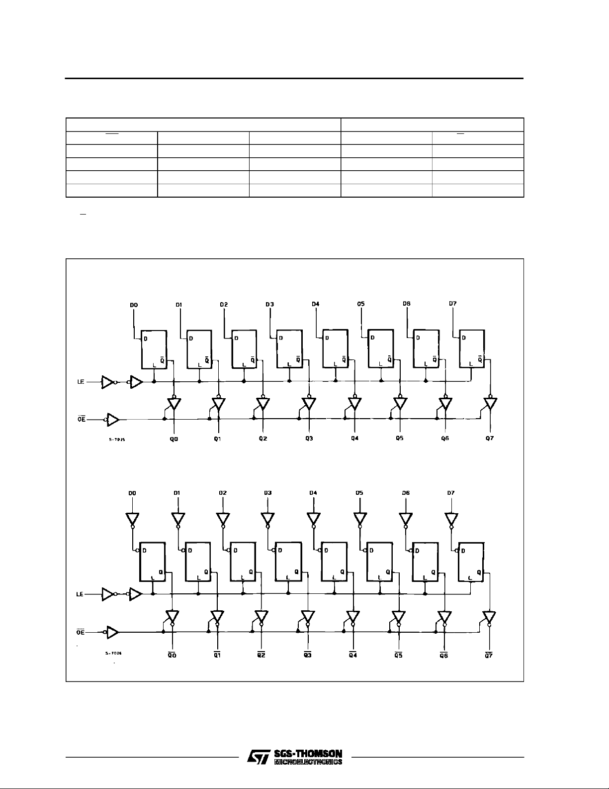
TRUTH TABLE
INPUTS OUTPUTS
OE LE D Q (HC373) Q (HC533)
HXXZZ
L L X NO CHANGE * NO CHANGE *
LHLLH
LHHHL
X: DON’T CARE
Z: HIGH IMPEDANCE
*: Q/Q OUTPUTS ARE LATCHED AT THETIMEWHENTHE LE INPUTIS TAKEN LOW LOGIC LEVEL.
LOGIC DIAGRAMS
HC373
M54/M74HC373/533
HC533
3/13
Page 4
M54/M74HC373/533
ABSOLU TE M AXIMU M R AT ING S
Symbol Parameter Value Unit
V
CC
V
V
O
I
IK
I
OK
I
O
I
or I
CC
P
D
T
stg
T
AbsoluteMaximumRatingsarethosevalues beyondwhichdamage tothedevice mayoccur.Functionaloperation under these conditionsisnot implied.
(*)500 mW: ≅ 65oC derateto300 mWby 10mW/oC: 65oCto85oC
RECO MM ENDED OPERAT I N G CO NDI TI O NS
Symbol Parameter Value Unit
V
CC
V
I
V
O
T
op
t
r,tf
Supply Voltage -0.5 to +7 V
DC Input Voltage -0.5 to VCC+ 0.5 V
I
DC Output Voltage -0.5 to VCC+ 0.5 V
DC Input Diode Current ± 20 mA
DC Output Diode Current ± 20 mA
DC Output Source Sink Current Per Output Pin ± 35 mA
DC VCCor Ground Current ± 70 mA
GND
Power Dissipation 500 (*) mW
Storage Temperature -65 to +150
Lead Temperature (10sec) 300
L
Supply Voltage 2 to 6 V
Input Voltage 0 to V
Output Voltage 0 to V
Operating Temperature: M54HC Series
M74HC Series
CC
CC
-55 to +125
-40 to +85
Input Rise and Fall Time VCC= 2 V 0 to 1000 ns
V
= 4.5 V 0 to 500
CC
V
= 6 V 0 to 400
CC
o
C
o
C
V
V
o
C
o
C
4/13
Page 5
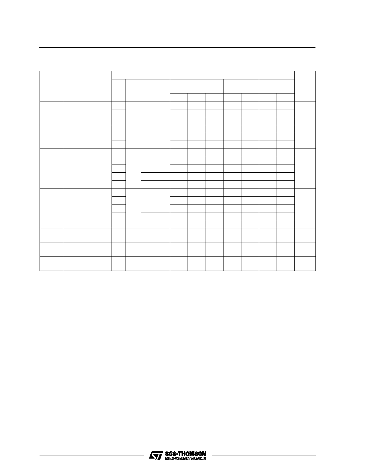
DC SPECIFICATIONS
Symbol Parameter
V
V
V
V
I
I
High Level Input
IH
Voltage
Low Level Input
IL
Voltage
High Level
OH
Output Voltage
Low Level Output
OL
Voltage
I
Input Leakage
I
Current
3 State Output
OZ
Off State Current
Quiescent Supply
CC
Current
M54/M74HC373/533
Test Conditions Value
T
=25oC
V
(V)
CC
A
54HC and 74HC
Min. Typ. Max. Min. Max. Min. Max.
2.0 1.5 1.5 1.5
4.5 3.15 3.15 3.15
6.0 4.2 4.2 4.2
2.0 0.5 0.5 0.5
4.5 1.35 1.35 1.35
6.0 1.8 1.8 1.8
2.0
4.5 4.4 4.5 4.4 4.4
6.0 5.9 6.0 5.9 5.9
4.5 I
6.0 I
2.0
4.5 0.0 0.1 0.1 0.1
6.0 0.0 0.1 0.1 0.1
4.5 I
6.0 I
6.0
=
V
I
IO=-20 µA
V
IH
or
V
IL
=-6.0 mA 4.18 4.31 4.13 4.10
O
=-7.8 mA 5.68 5.8 5.63 5.60
O
V
=
I
IO=20µA
V
IH
or
V
IL
= 6.0 mA 0.17 0.26 0.33 0.40
O
= 7.8 mA 0.18 0.26 0.33 0.40
O
VI=VCCor GND ±0.1 ±1 ±1 µA
6.0 VI=VIHor V
1.9 2.0 1.9 1.9
0.0 0.1 0.1 0.1
IL
VO=VCCor GND
6.0 VI=VCCor GND 4 40 80 µA
-40 to 85oC
74HC
-55 to 125oC
54HC
Unit
±0.5 ±5.0 ±10 µA
V
V
V
V
5/13
Page 6
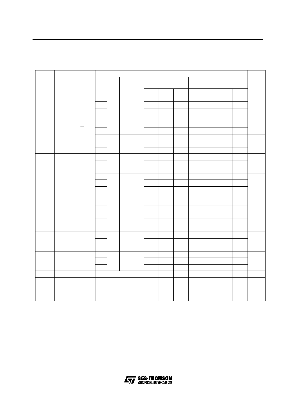
M54/M74HC373/533
AC ELECTRICAL CHARACTERISTICS (CL=50pF,Inputtr=tf=6ns)
Test Conditions Value
T
=25oC
Symbol Parameter
t
t
TLH
THL
Output Transition
Time
C
V
CC
(V)
L
(pF)
2.0
50
4.5 7121518
A
54HC and 74HC
Min. Typ. Max. Min. Max. Min. Max.
25 60 75 90
6.0 6101315
t
PLH
t
PHL
Propagation
Delay Time
(LE, D - Q, Q)
2.0
50
4.5 14 25 31 38
42 125 155 190
6.0 12 21 26 32
2.0
150
4.5 19 35 44 53
57 175 220 265
6.0 16 30 37 45
t
t
PZL
PZH
3 State Output
Enable Time
2.0
50 RL=1KΩ
4.5 13 25 31 38
39 125 155 190
6.0 11 21 26 32
2.0
150 R
4.5 18 35 44 53
=1KΩ
L
54 175 220 265
6.0 15 30 37 45
t
t
PLZ
PHZ
3 State Output
Disable Time
2.0
50 RL=1KΩ
4.5 14 25 31 38
30 125 155 190
6.0 13 21 26 32
t
W(H)
Minimum Pulse
Width (LE)
2.0
50
4.5 6151922
15 75 95 110
6.0 6131619
Minimum Set-up
t
s
Time
2.0
50
4.5 4101315
16 50 65 75
6.0 3 9 11 13
t
h
Minimum Hold
Time
2.0
50
4.5 5 5 5
6.0 5 5 5
C
C
Input Capacitance 5 10 10 10 pF
IN
OUT
Out put
10
Capacitance
(*) Power Dissipation
C
PD
38
Capacitance
(*) CPDisdefined as thevalueof the IC’sinternal equivalent capacitance which is calculated from the operating current consumption withoutload.
(Refer to TestCircuit).Averageoperting current can be obtainedby thefollowingequation. ICC(opr) = CPD• VCC•fIN+ICC/8(per Flip Flop) andthe
CPDwhenn pcsofFlip Flopoperate, canbe gainedby following equation: CPD(TOTAL) =22 +16 x n [pF]
-40 to 85oC
74HC
-55 to 125oC
54HC
Unit
ns
ns
ns
ns
ns
ns
ns
ns
555
ns
pF
pF
6/13
Page 7

SWITCHING CHARACTERISTICS TEST WAVEFORM
M54/M74HC373/533
t
PLH,tPHL
t
PLZ,tPZL
, (D - Q, Q) t
The 1KΩ load resistors should be connected between
outputs and VCCline and the 50pF load capacitors
should be connected between outputsand GND line.
All inputs except OE input should be connected to V
CC
line or GND line such that outputs will be in low logic
level while OE input is held low.
PLH,tPHL
t
PHZ,tPZH
(LE - Q, Q), ts,th,t
W
The 1KΩ load resistors and the 50pF load capacitors
should be connected between each output and GND
line.
All inputs except OE input should be connected to V
CC
or GND line such that output will be in high logic level
while OE input is held low.
7/13
Page 8

M54/M74HC373/533
TEST CIRCUIT ICC(Opr.)
INPUTWAVEFORM ISTHE SAME AS THATIN CASEOF SWITCHINGCHARACTERISTICSTEST.
8/13
Page 9

Plastic DIP20 (0.25) MECHANICAL DATA
M54/M74HC373/533
DIM.
MIN. TYP. MAX. MIN. TYP. MAX.
a1 0.254 0.010
B 1.39 1.65 0.055 0.065
b 0.45 0.018
b1 0.25 0.010
D 25.4 1.000
E 8.5 0.335
e 2.54 0.100
e3 22.86 0.900
F 7.1 0.280
I 3.93 0.155
L 3.3 0.130
Z 1.34 0.053
mm inch
P001J
9/13
Page 10

M54/M74HC373/533
Ceramic DIP20 MECHANICAL DATA
DIM.
MIN. TYP. MAX. MIN. TYP. MAX.
A 25 0.984
B 7.8 0.307
D 3.3 0.130
E 0.5 1.78 0.020 0.070
e3 22.86 0.900
F 2.29 2.79 0.090 0.110
G 0.4 0.55 0.016 0.022
I 1.27 1.52 0.050 0.060
L 0.22 0.31 0.009 0.012
M 0.51 1.27 0.020 0.050
N1 4° (min.), 15° (max.)
P 7.9 8.13 0.311 0.320
Q 5.71 0.225
mm inch
10/13
P057H
Page 11

SO20 MECHANICAL DATA
M54/M74HC373/533
DIM.
MIN. TYP. MAX. MIN. TYP. MAX.
A 2.65 0.104
a1 0.10 0.20 0.004 0.007
a2 2.45 0.096
b 0.35 0.49 0.013 0.019
b1 0.23 0.32 0.009 0.012
C 0.50 0.020
c1 45° (typ.)
D 12.60 13.00 0.496 0.512
E 10.00 10.65 0.393 0.419
e 1.27 0.050
e3 11.43 0.450
F 7.40 7.60 0.291 0.299
L 0.50 1.27 0.19 0.050
M 0.75 0.029
S8°(max.)
mm inch
P013L
11/13
Page 12

M54/M74HC373/533
PLCC20 MECHANICAL DATA
DIM.
MIN. TYP. MAX. MIN. TYP. MAX.
A 9.78 10.03 0.385 0.395
B 8.89 9.04 0.350 0.356
D 4.2 4.57 0.165 0.180
d1 2.54 0.100
d2 0.56 0.022
E 7.37 8.38 0.290 0.330
e 1.27 0.050
e3 5.08 0.200
F 0.38 0.015
G 0.101 0.004
M 1.27 0.050
M1 1.14 0.045
mm inch
12/13
P027A
Page 13

M54/M74HC373/533
Information furnishedis believed to be accurate and reliable. However, SGS-THOMSON Microelectronicsassumes no responsabilityfor the
consequences of useof suchinformation nor for any infringementof patents or other rightsof third parties which may results from its use. No
license is granted byimplication or otherwiseunder any patentor patentrights ofSGS-THOMSON Microelectronics. Specificationsmentioned
in thispublication are subjectto changewithout notice. This publicationsupersedes andreplaces all information previouslysupplied.
SGS-THOMSON Microelectronicsproducts are not authorized foruse ascritical componentsin life supportdevices or systems without express
written approval of SGS-THOMSON Microelectonics.
1994SGS-THOMSON Microelectronics- All Rights Reserved
Australia -Brazil - France - Germany - Hong Kong - Italy -Japan - Korea -Malaysia - Malta - Morocco - The Netherlands -
Singapore -Spain - Sweden- Switzerland - Taiwan - Thailand - UnitedKingdom -U.S.A
SGS-THOMSON Microelectronics GROUP OFCOMPANIES
13/13
 Loading...