

Page 1
HC365 NON INVERTING - HC366 INVERTING
.HIGH SPEED
tPD= 9 ns (TYP) AT VCC=5V
.LOWPOWER DISSIPATION
ICC=4µA(MAX.) AT TA=25°C
.HIGH NOISEIMMUNITY
V
NIH=VNIL
=28%VCC(MIN.)
.OUTPUT DRIVE CAPABILITY
15 LSTTL LOADS
.SYMMETRICAL OUTPUT IMPEDANCE
|IOH|=IOL=6 mA (MIN.)
.BALANCEDPROPAGATION DELAYS
t
PLH=tPHL
.WIDE OPERATING VOLTAGE RANGE
VCC(OPR)= 2 V TO 6 V
.PIN AND FUNCTION COMPATIBLE WITH
54/74LS365/366
M54/M74HC365
M54/M74HC366
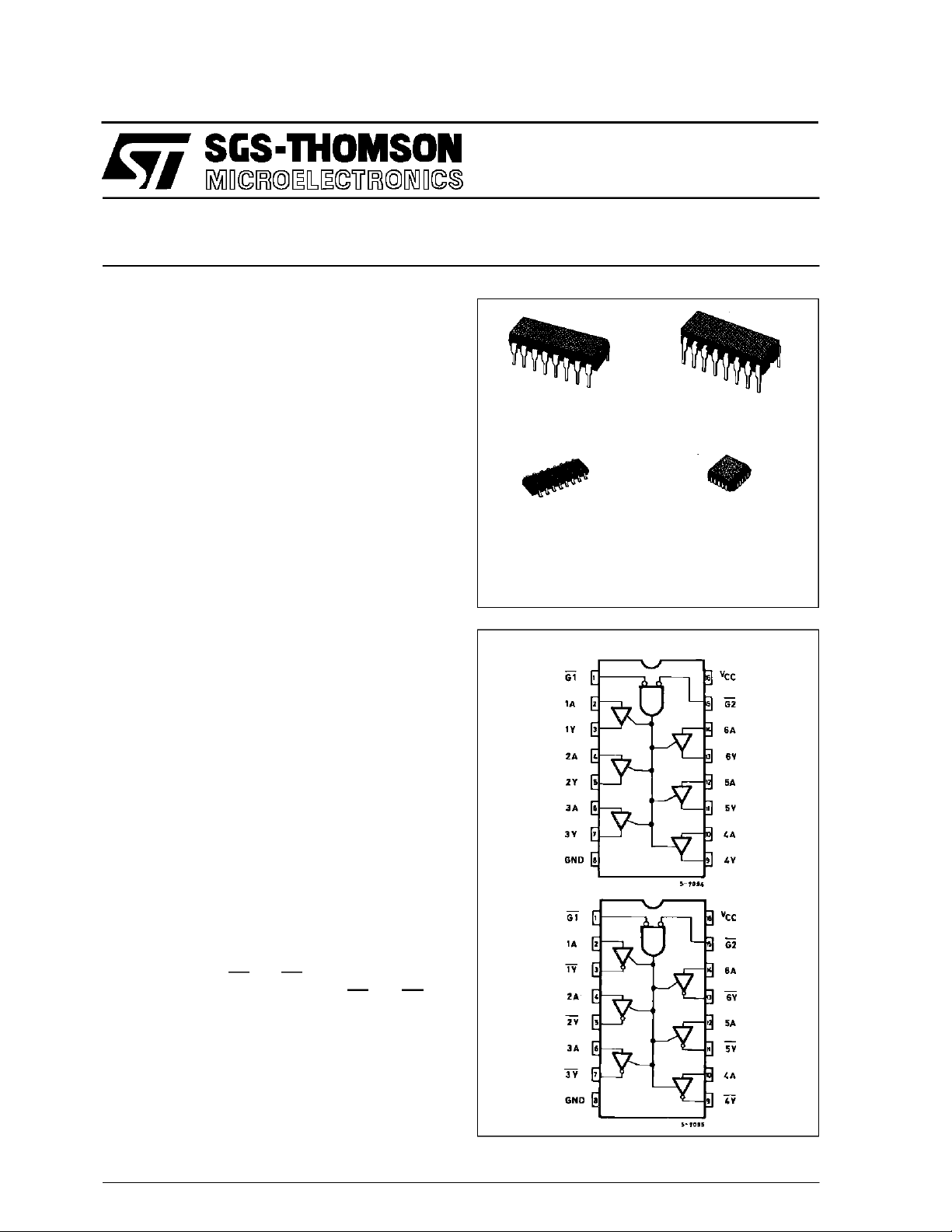
HEX BUS BUFFER (3-STATE)
B1R
(PlasticPackage)
M1R
(MicroPackage)
ORDER CODES :
M54HC X XXF1R M74H CXXXM1R
M74HC X XXB1R M 74H CXXXC1R
F1R
(CeramicPackage)
C1R
(Chip Carrier)
DESCRIPTION
The M54/74HC365 andtheM54/74HC366arehigh
speedCMOS HEX BUSBUFFER fabricated in silicon gate C2MOS technology. Theyhave the same
high speed performance of LSTTL combined with
true CMOS low power consumption.
All six buffers are controlled by the combination of
two enable inputs(G1 and G2); alloutputs of these
buffers areenabled only when both G1 and G2 inputs are held low, under all other conditions these
outputare disabled to be high-impedance.
Theseoutputsarecapableofdriving upto15LSTTL
loads. The designer has a choice of non-inverting
outputs(HC365)and inverting outputs (HC366).All
inputs areequipped with protection circuits against
staticdischarge andtransient excess voltage.
PIN CONNECTIONS(top view)
HC365
HC366
October 1992
1/11
Page 2
M54/M74HC365/366
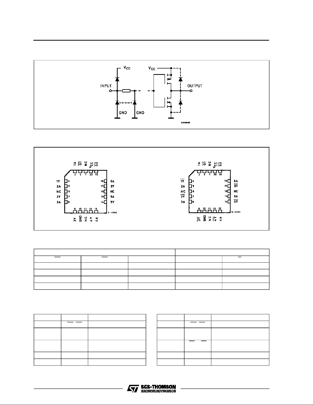
INPUT AND OUTPUT EQUIVALENT CIRCUIT
CHIP CARRIER
HC365 HC366
TRUTH TABLE
INPUTS OUTPUTS
G1 G2 An Y (365) Y (366)
LLLLH
LLHHL
HXXZZ
XHXZZ
X = DON’TCARE Z= HIGHIMPEDANCE
PIN DESCRIPTION (HC365)
PIN No SYMBOL NAME AND FUNCTION
1, 15 G1, G2 Output Enable Inputs
2, 4, 6, 10,
12, 14
3, 5, 7, 9,
11, 13
8 GND Ground (0V)
16 V
1A to 6A Data Inputs
1Y to 6Y Data Outputs
CC
Positive Supply Voltage
NC = No Internal Connection
PIN DESCRIPTION (HC366)
PIN No SYMBOL NAME AND FUNCTION
1, 15 G1, G2 Output Enable Inputs
2, 4, 6, 10,
12, 14
3, 5, 7, 9,
11, 13
8 GND Ground (0V)
16 V
1A to 6A Data Inputs
1Y to 6Y Data Outputs
CC
Positive Supply Voltage
2/11
Page 3
M54/M74HC365/366
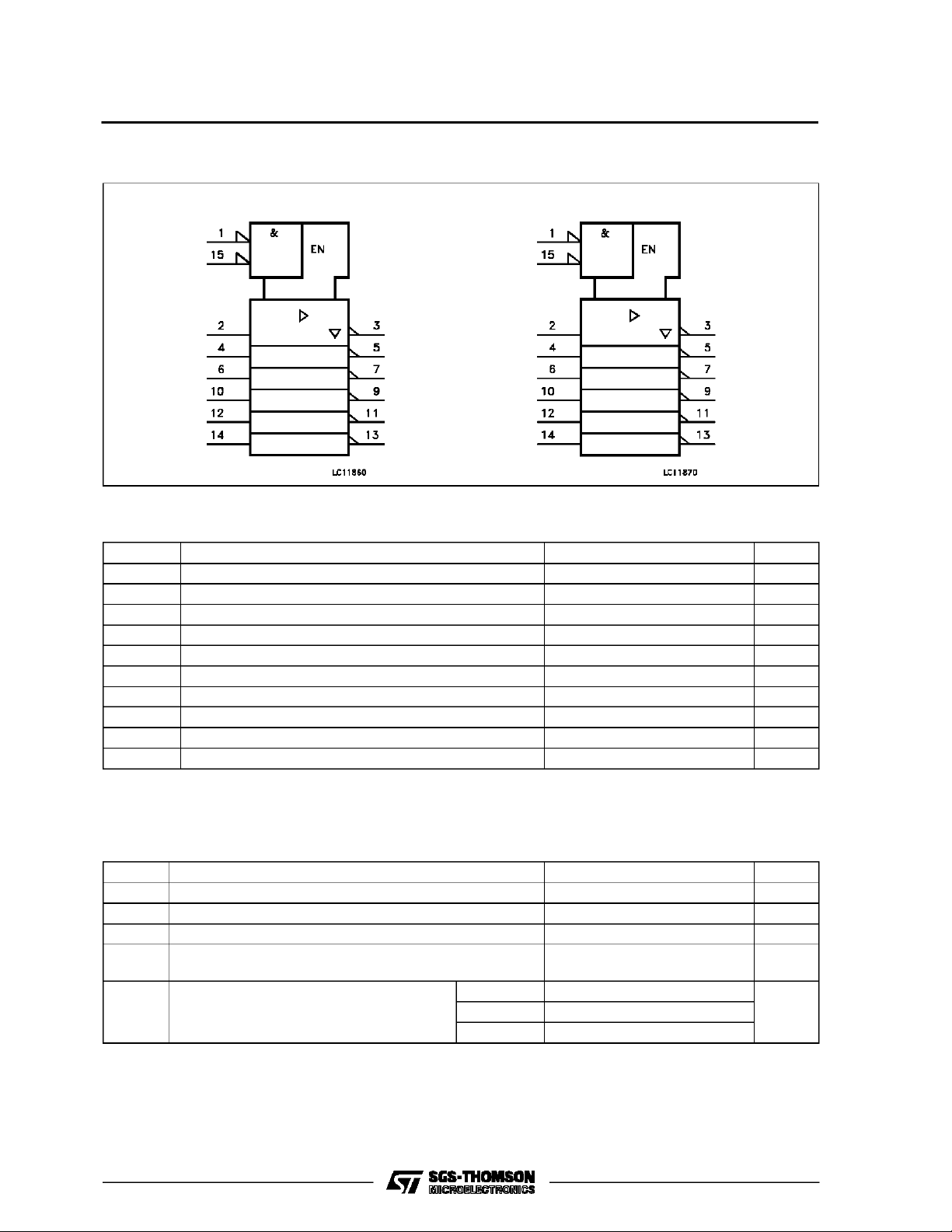
IEC LOGIC SYMBOL
HC365 HC366
ABSOLU TE MAXI MU M RAT I NG S
Symbol Parameter Value Unit
V
CC
V
V
O
I
IK
I
OK
I
O
I
or I
CC
P
D
T
stg
T
AbsoluteMaximumRatingsarethosevalues beyond whichdamage tothedevicemayoccur.Functional operationunder theseconditionisnotimplied.
(*)500 mW: ≅ 65oC derate to300mW by 10mW/oC: 65oCto85oC
Supply Voltage -0.5 to +7 V
DC Input Voltage -0.5 to VCC+ 0.5 V
I
DC Output Voltage -0.5 to VCC+ 0.5 V
DC Input Diode Current ± 20 mA
DC Output Diode Current ± 20 mA
DC Output Source Sink Current Per Output Pin ± 35 mA
DC VCCor Ground Current ± 70 mA
GND
Power Dissipation 500 (*) mW
Storage Temperature -65 to +150
Lead Temperature (10 sec) 300
L
o
C
o
C
RECO MM ENDED OPERATIN G CO NDI TIONS
Symbol Parameter Value Unit
V
T
t
V
V
r,tf
Supply Voltage 2 to 6 V
CC
Input Voltage 0 to V
I
Output Voltage 0 to V
O
Operating Temperature: M54HC Series
op
M74HC Series
CC
CC
-55 to +125
-40 to +85
Input Rise and Fall Time VCC= 2 V 0 to 1000 ns
V
= 4.5 V 0 to 500
CC
V
= 6 V 0 to 400
CC
V
V
o
C
o
C
3/11
Page 4
M54/M74HC365/366
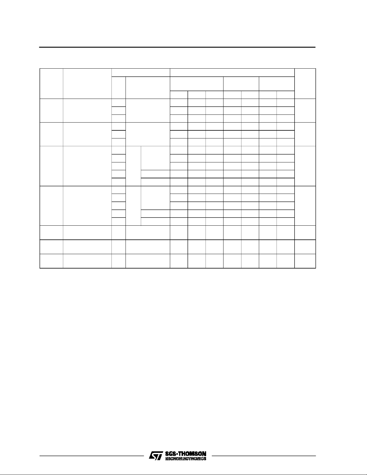
DC SPECIFICATIONS
Symbol Parameter
V
V
V
V
I
I
High Level Input
IH
Voltage
Low Level Input
IL
Voltage
High Level
OH
Output Voltage
Low Level Output
OL
Voltage
I
Input Leakage
I
Current
3 State Output
OZ
Off State Current
Quiescent Supply
CC
Current
Test Conditions Value
V
(V)
CC
=25oC
A
54HC and 74HC
Min. Typ. Max. Min. Max. Min. Max.
-40 to 85oC
74HC
-55 to 125oC
54HC
Unit
T
2.0 1.5 1.5 1.5
4.5 3.15 3.15 3.15
6.0 4.2 4.2 4.2
2.0 0.5 0.5 0.5
4.5 1.35 1.35 1.35
6.0 1.8 1.8 1.8
2.0
4.5 4.4 4.5 4.4 4.4
6.0 5.9 6.0 5.9 5.9
4.5 I
6.0 I
2.0
4.5 0.0 0.1 0.1 0.1
6.0 0.0 0.1 0.1 0.1
4.5 I
6.0 I
6.0
6.0
=
V
I
IO=-20 µA
V
IH
or
V
IL
=-6.0 mA 4.18 4.31 4.13 4.10
O
=-7.8 mA 5.68 5.8 5.63 5.60
O
=
V
I
IO=20µA
V
IH
or
V
IL
= 6.0 mA 0.17 0.26 0.33 0.40
O
= 7.8 mA 0.18 0.26 0.33 0.40
O
VI=VCCor GND ±0.1 ±1 ±1 µA
VI=VIHor V
VO=VCCor GND
1.9 2.0 1.9 1.9
0.0 0.1 0.1 0.1
IL
±0.5 ±5 ±10 µA
6.0 VI=VCCor GND 4 40 80 µA
V
V
V
V
4/11
Page 5

M54/M74HC365/366
AC ELECTRICAL CHARACTERISTICS (CL=50pF,Inputtr=tf=6ns)
Test Conditions Value
T
=25oC
Symbol Parameter
t
t
TLH
THL
Output Transition
Time
V
C
CC
(V)
L
(pF)
2.0
50
4.5 7121518
A
54HC and 74HC
Min. Typ. Max. Min. Max. Min. Max.
25 60 75 90
6.0 6101315
t
PLH
t
PHL
Propagation
Delay Time
2.0
50
4.5 12 18 23 27
38 90 115 135
6.0 10 15 20 23
2.0
150
4.5 17 26 33 39
51 130 165 195
6.0 14 22 28 33
t
t
PZH
PZL
Output Enable
Time
2.0
50 RL=1KΩ
4.5 16 26 33 39
64 130 165 195
6.0 14 22 28 33
2.0
150 R
4.5 19 30 38 45
=1KΩ
L
76 150 190 225
6.0 16 26 32 38
t
t
PHZ
PLZ
Output Disable
Time
2.0
50 RL=1KΩ
4.5 18 26 33 39
42 130 165 195
6.0 15 22 28 33
C
C
PD
(*) CPDisdefined asthe valueof the IC’s internal equivalent capacitance whichis calculated fromthe operating current consumption withoutload.
(Referto TestCircuit). Average operting current can be obtained bythe followingequation. ICC(opr) = CPD•VCC•fIN+ICC/6(per Gate)
Input Capacitance 5 10 10 10 pF
IN
(*) Power Dissipation
Capacitance
for HC365
for HC366
27
25
-40 to 85oC
74HC
-55 to 125oC
54HC
Unit
ns
ns
ns
ns
ns
ns
pF
TEST CIRCUIT ICC(Opr.)
INPUT WAVEFORM IS THE SAME AS THAT IN CASE OF
SWITCHINGCHARACTERISTICSTEST.
CPDCALCULATION
CPDis to be calculated with the following
formula by using the measured value of
ICC (opr.) in the testcircuit opposite.
I
(
opr
CPD=
f
CC
IN
)
×
V
CC
In determining the typicalvalue of CPD a
relatvelyhigh frequency of 1MHzwas appliedto fIN, in order to eliminate any error
causedby the quiescent supplycurrent.
5/11
Page 6

M54/M74HC365/366
SWITCHING CHARACTERISTICS TEST WAVEFORM
GND
V
CC
Note: Sucha logic level shallbeapplied toeach inputthatthe outputvoltagestaysin theapposite side to the switch connection level, when
the output is enable.
6/11
Page 7

Plastic DIP16 (0.25) MECHANICAL DATA
M54/M74HC365/366
DIM.
MIN. TYP. MAX. MIN. TYP. MAX.
a1 0.51 0.020
B 0.77 1.65 0.030 0.065
b 0.5 0.020
b1 0.25 0.010
D 20 0.787
E 8.5 0.335
e 2.54 0.100
e3 17.78 0.700
F 7.1 0.280
I 5.1 0.201
L 3.3 0.130
Z 1.27 0.050
mm inch
P001C
7/11
Page 8

M54/M74HC365/366
Ceramic DIP16/1 MECHANICAL DATA
DIM.
MIN. TYP. MAX. MIN. TYP. MAX.
A 20 0.787
B 7 0.276
D 3.3 0.130
E 0.38 0.015
e3 17.78 0.700
F 2.29 2.79 0.090 0.110
G 0.4 0.55 0.016 0.022
H 1.17 1.52 0.046 0.060
L 0.22 0.31 0.009 0.012
M 0.51 1.27 0.020 0.050
N 10.3 0.406
P 7.8 8.05 0.307 0.317
Q 5.08 0.200
mm inch
8/11
P053D
Page 9

SO16 (Narrow) MECHANICAL DATA
M54/M74HC365/366
DIM.
MIN. TYP. MAX. MIN. TYP. MAX.
A 1.75 0.068
a1 0.1 0.2 0.004 0.007
a2 1.65 0.064
b 0.35 0.46 0.013 0.018
b1 0.19 0.25 0.007 0.010
C 0.5 0.019
c1 45° (typ.)
D 9.8 10 0.385 0.393
E 5.8 6.2 0.228 0.244
e 1.27 0.050
e3 8.89 0.350
F 3.8 4.0 0.149 0.157
G 4.6 5.3 0.181 0.208
L 0.5 1.27 0.019 0.050
M 0.62 0.024
S8°(max.)
mm inch
P013H
9/11
Page 10

M54/M74HC365/366
PLCC20 MECHANICAL DATA
DIM.
MIN. TYP. MAX. MIN. TYP. MAX.
A 9.78 10.03 0.385 0.395
B 8.89 9.04 0.350 0.356
D 4.2 4.57 0.165 0.180
d1 2.54 0.100
d2 0.56 0.022
E 7.37 8.38 0.290 0.330
e 1.27 0.050
e3 5.08 0.200
F 0.38 0.015
G 0.101 0.004
M 1.27 0.050
M1 1.14 0.045
mm inch
10/11
P027A
Page 11

M54/M74HC365/366
Information furnished isbelieved tobe accurate and reliable.However, SGS-THOMSON Microelectronicsassumes no responsability for the
consequences of use of such information nor for any infringementof patents or other rights of third partieswhich may results from its use. No
license is granted byimplication or otherwiseunderany patentor patent rights ofSGS-THOMSON Microelectronics. Specificationsmentioned
in this publicationare subject to changewithout notice. This publication supersedes and replaces all informationpreviously supplied.
SGS-THOMSON Microelectronicsproductsare notauthorizedforuse ascritical componentsinlife support devices orsystemswithout express
written approval of SGS-THOMSONMicroelectonics.
1994SGS-THOMSON Microelectronics- All RightsReserved
Australia - Brazil- France - Germany - HongKong - Italy- Japan - Korea - Malaysia -Malta - Morocco - The Netherlands-
Singapore - Spain - Sweden - Switzerland - Taiwan - Thailand - United Kingdom - U.S.A
SGS-THOMSON Microelectronics GROUP OF COMPANIES
11/11
 Loading...