

Page 1
8 CHANNEL MULTIPLEXER/REGISTER (3 STATE)
.HIGH SPEED
tPD= 24 ns(TYP.) AT VCC=5V
.LOWPOWER DISSIPATION
ICC=4µA(MAX.) AT TA=25°C
.HIGH NOISEIMMUNITY
V
NIH=VNIL
=28%VCC(MIN.)
.OUTPUT DRIVE CAPABILITY
15 LSTTL LOADS
.SYMMETRICAL OUTPUT IMPEDANCE
|IOH|=IOL=6 mA (MIN.)
.BALANCEDPROPAGATION DELAYS
t
PLH=tPHL
.WIDE OPERATING VOLTAGE RANGE
VCC(OPR)= 2 V TO 6 V
.PIN AND FUNCTION COMPATIBLE
WITH 54/74LS354
M54HC354
M74HC354
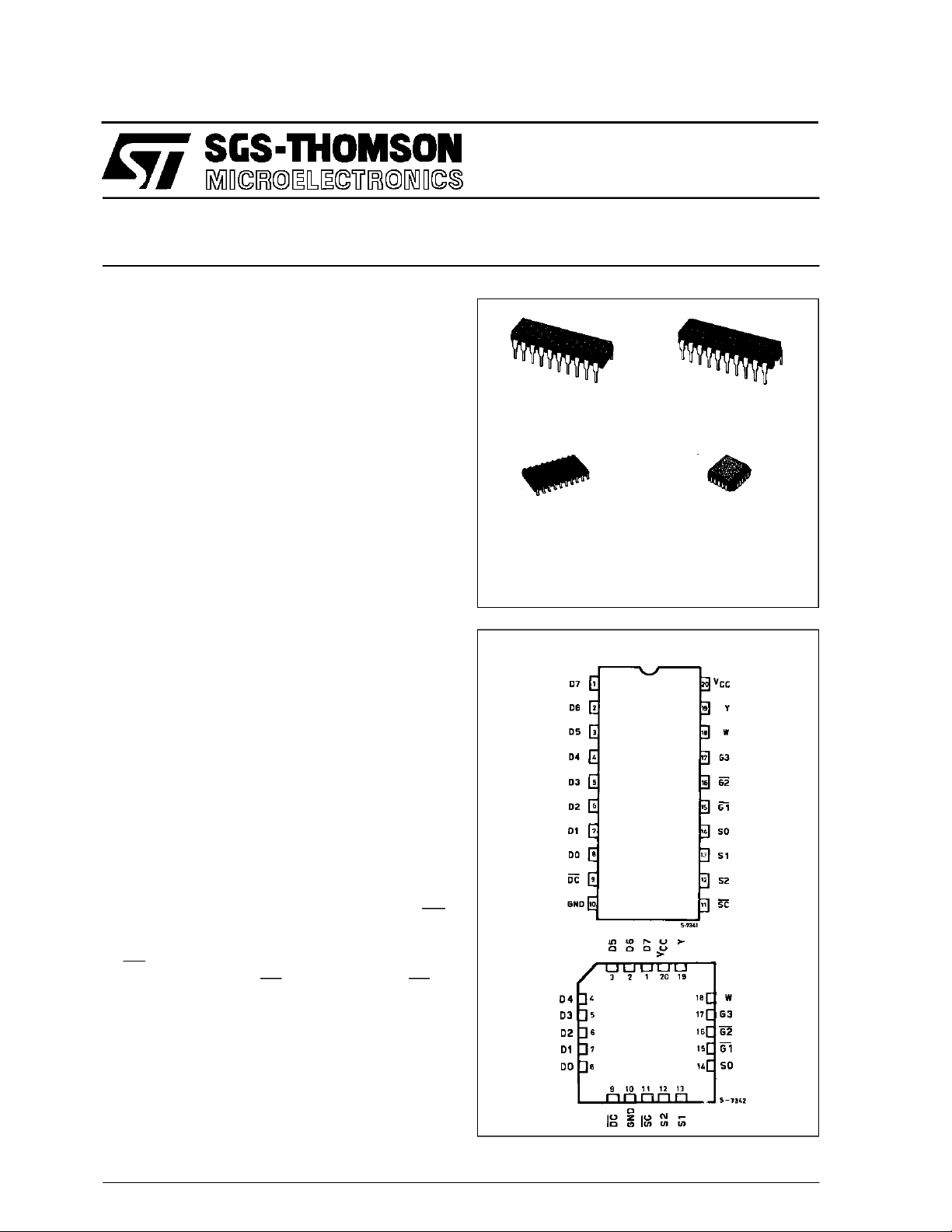
B1R
(PlasticPackage)
M1R
(MicroPackage)
ORDER CODES :
M54HC 354F1R M74H C354M1R
M74HC 354B1R M74HC3 54C1R
F1R
(CeramicPackage)
C1R
(Chip Carrier)
DESCRIPTION
TheM54/74HC354is ahighspeed CMOS8-CHANNEL MULTIPLEXER/REGISTER (3-state) fabricated in silicongate C2MOS technology. It has the
same high speed performance of LSTTL combined
with trueCMOS low consumption.
Thisdevicecontains an 8channeldigitalmultiplexer
with an8-bit inputdata registerand a 3-bit address
inputregisterwith 3-state outputs. The one of eight
inputdata will be provided on the Y output pin (noninverted output) and W output pin(inverted output)
determined by the addressdata.
The information at the data inputs (D0 to D7) is
storedin the 8-bit latchat the negative pulse on DC
input. The informationat the address inputs (S0 to
S2) isstored in the 3-bitlatch at the negative pulse
on SCinput. Theseoutputsare disabled to behighimpedance when input G1 is heldhigh, input G2 is
heldhigh orinputG3 is held low.Thisdeviceissuitablefor interfacing withbuslinesin a busorganized
system.
The M54/74HC354 is similar in function to the
M54/74HC356, which has an 8-bit flip-flop as the
data register instead of an 8-bit latch.All inputs are
equipped with protection circuits against static discharge and transientexcess voltage.
PIN CONNECTIONS(top view)
NC =
No Internal
Connection
April1993
1/12
Page 2
M54/M74HC354
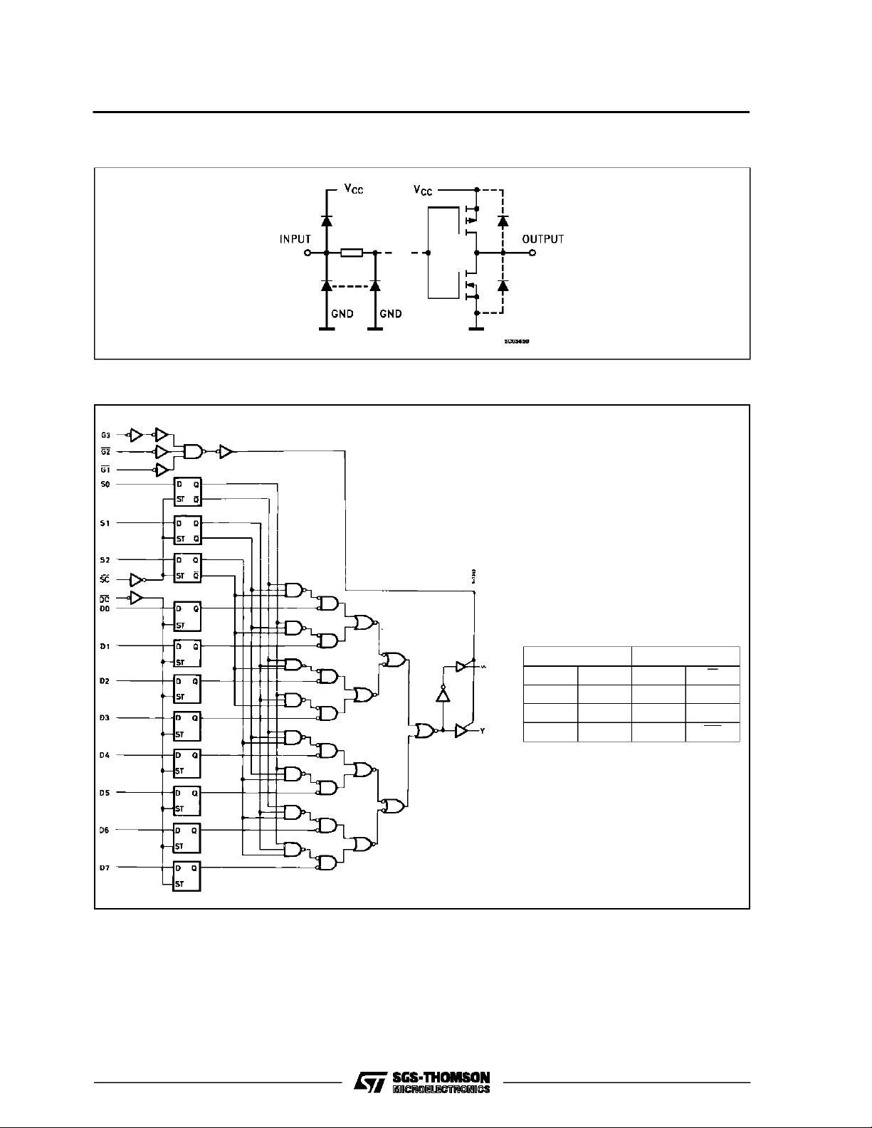
INPUT AND OUTPUT EQUIVALENT CIRCUIT
LOGIC DIAGRAM
TRUT H TABLE OF INTERNAL LAT CH
INPUTS OUTPUTS
DSTQ Q
LHLH
HHHL
X L Qn Qn
X:DON’TCARE
Qn:DATA STORED AT THE TRAILINGEDGE
OFTHE MOSTRECENTST PULSE.
2/12
Page 3
M54/M74HC354
TRUTH TABLE
INPUTS OUTPUTS
SELECT *
S2 S1 S0 G1 G2 G3
XXXXHXXZZ
XXXXXHXZZ
XXXXXXLZZ
LLLLLLHD0D0
L L L H L L H D0n D0n
LLHLLLHD1D1
L L H H L L H D1n D1n
L H L L L L H D2 D2
LHLHLLHD2nD2n
LHHLLLHD3D3
L H H H L L H D3n D3n
HLLLLLHD4D4
H L L H L L H D4n D4n
HLHLLLHD5D5
H L H H L L H D5n D5n
HHLLLLHD6D6
HHLHLLHD6nD6n
HHHLL LHD7D7
H H H H L L H D7n D7n
X:DON’TCARE Z:HIGHIMPEDANCE *:THISCOLUMNSHOWSTHEINPUTADDRESSSETUPWITHSC LOW
D0n....D7n:THELEVELOFSTEADY-STATEINPUTSAT INPUTDOTHROUGH D7,RESPECTIVELY,BEFORETHEMOSTRECENT LOWTO
HIGHTRANSITIONOFDATA CONTROL.
DC
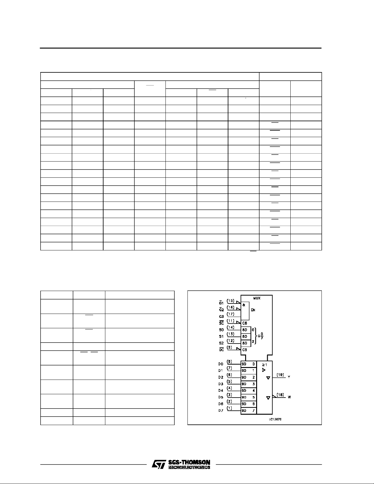
OUTPUT ENABLES
WY
PIN DESCRIPTION
PIN No SYMBOL NAME AND FUNCTION
8, 7, 6, 5,
4, 3, 2, 1
9 DC Data Enable Input (Active
11 SC Latch Enable Input
14, 13, 12 SO, S1, S2 Select Inputs
15, 16 G1, G2 Output Enable Inputs
17 G3 Output Enable Input
18 W 3 State Multiplexer Output
19 Y 3 State Multiplexer Output
10 GND Ground (0V)
20 V
D0 to D7 Data Inputs
LOW)
(Active LOW)
(Active LOW)
(Active HIGH)
(Active LOW)
(Active HIGH)
CC
Positive Supply Voltage
IEC LOGIC SYMBOL
3/12
Page 4
M54/M74HC354
ABSOLU TE M AXIMU M R AT ING
Symbol Parameter Value Unit
V
CC
V
V
O
I
IK
I
OK
I
O
I
or I
CC
P
D
T
stg
T
AbsoluteMaximumRatingsarethose values beyond whichdamage tothedevicemayoccur.Functional operationunder theseconditionisnotimplied.
(*)500 mW:≅ 65oC derate to300 mW by 10mW/oC: 65oCto85oC
RECO MM ENDED OPERATI N G CO NDI TIONS
Symbol Parameter Value Unit
V
CC
V
I
V
O
T
op
t
r,tf
Supply Voltage -0.5 to +7 V
DC Input Voltage -0.5 to VCC+ 0.5 V
I
DC Output Voltage -0.5 to VCC+ 0.5 V
DC Input Diode Current ± 20 mA
DC Output Diode Current ± 20 mA
DC Output Source Sink Current Per Output Pin ± 35 mA
DC VCCor Ground Current ± 70 mA
GND
Power Dissipation 500 (*) mW
Storage Temperature -65 to +150
Lead Temperature (10 sec) 300
L
Supply Voltage 2 to 6 V
Input Voltage 0 to V
Output Voltage 0 to V
Operating Temperature: M54HC Series
M74HC Series
CC
CC
-55 to +125
-40 to +85
Input Rise and Fall Time VCC= 2 V 0 to 1000 ns
V
= 4.5 V 0 to 500
CC
V
= 6 V 0 to 400
CC
o
C
o
C
V
V
o
C
o
C
4/12
Page 5

DC SPECIFICATIONS
Symbol Parameter
V
V
V
V
I
I
High Level Input
IH
Voltage
Low Level Input
IL
Voltage
High Level
OH
Output Voltage
Low Level Output
OL
Voltage
I
Input Leakage
I
Current
3 State Output
OZ
Off State Current
Quiescent Supply
CC
Current
M54/M74HC354
Test Conditions Value
T
=25oC
V
(V)
CC
A
54HC and 74HC
Min. Typ. Max. Min. Max. Min. Max.
2.0 1.5 1.5 1.5
4.5 3.15 3.15 3.15
6.0 4.2 4.2 4.2
2.0 0.5 0.5 0.5
4.5 1.35 1.35 1.35
6.0 1.8 1.8 1.8
2.0
4.5 4.4 4.5 4.4 4.4
6.0 5.9 6.0 5.9 5.9
4.5 I
6.0 I
2.0
4.5 0.0 0.1 0.1 0.1
6.0 0.0 0.1 0.1 0.1
4.5 I
6.0 I
6.0
=
V
I
IO=-20 µA
V
IH
or
V
IL
=-6.0 mA 4.18 4.31 4.13 4.10
O
=-7.8 mA 5.68 5.8 5.63 5.60
O
V
=
I
IO=20µA
V
IH
or
V
IL
= 6.0 mA 0.17 0.26 0.33 0.40
O
= 7.8 mA 0.18 0.26 0.33 0.40
O
VI=VCCor GND ±0.1 ±1 ±1 µA
6.0 VI=VIHor V
1.9 2.0 1.9 1.9
0.0 0.1 0.1 0.1
IL
VO=VCCor GND
6.0 VI=VCCor GND 4 40 80 µA
-40 to 85oC
74HC
-55 to 125oC
54HC
Unit
±0.5 ±5.0 ±10 µA
V
V
V
V
5/12
Page 6

M54/M74HC354
AC ELECTRICAL CHARACTERISTICS (CL=50pF,Inputtr=tf=6ns)
Test Conditions Value
T
=25oC
Symbol Parameter
t
t
TLH
THL
Output Transition
Time
V
C
CC
(V)
L
(pF)
2.0
50
4.5 7121518
A
54HC and 74HC
Min. Typ. Max. Min. Max. Min. Max.
25 60 75 90
6.0 6101315
t
PLH
t
PHL
Propagation
Delay Time
(Dn, DC - Y, W)
2.0
50
4.5 26 42 53 63
83 210 265 315
6.0 21 36 45 54
2.0
150
4.5 31 50 63 75
99 250 315 375
6.0 25 43 54 64
t
t
PLH
PHL
Propagation
Delay Time
(Sn - Y, W)
2.0
50
4.5 30 52 65 78
98 260 325 390
6.0 25 44 55 66
2.0
150
4.5 35 60 75 90
114 300 375 450
6.0 29 51 64 77
t
t
PLH
PHL
Propagation
Delay Time
(SC - Y, W)
2.0
50
4.5 31 54 68 81
102 270 340 405
6.0 27 46 58 69
2.0
150
4.5 36 62 78 93
118 310 390 465
6.0 31 53 66 79
t
t
PZH
PZL
3 State Output
Enable Time
2.0
50 R
4.5 14 25 31 38
=1KΩ
L
44 125 155 190
6.0 12 21 26 32
2.0
150 R
4.5 19 33 41 50
=1KΩ
L
60 165 205 250
6.0 16 28 35 43
t
t
PHZ
PLZ
3 State Output
Disable Time
2.0
50 RL=1KΩ
4.5 20 31 39 47
42 155 195 235
6.0 17 26 33 40
t
W(L)
Minimum Pulse
Width (DC) (SC)
2.0
50
4.5 6151922
18 75 95 110
6.0 6131619
Minimum Set-up
t
s
Time (Dn) (Sn)
2.0
50
4.5 3101315
10 50 65 75
6.0 3 9 11 13
t
h
Minimum Hold
Time (Dn) (Sn)
2.0
50
4.5 5 5 5
6.0 5 5 5
C
C
PD
Input Capacitance 5 10 10 10 pF
IN
(*) Power Dissipation
77
Capacitance
(*) CPDisdefined asthe value of the IC’s internal equivalent capacitance whichis calculated from the operating current consumption without load.
(RefertoTest Circuit).Average operting current can be obtained bythe followingequation. ICC(opr) = CPD•VCC•fIN+I
-40 to 85oC
74HC
-55 to 125oC
54HC
Unit
ns
ns
ns
ns
ns
ns
ns
ns
ns
ns
ns
ns
555
ns
pF
CC
6/12
Page 7

TEST CIRCUIT ICC(Opr.)
INPUT WAVEFORMIS THE SAME AS THAT IN CASEOF SWITCHING CHARACTERISTICS TEST.
SWITCHING CHARACTERISTICS TEST WAVEFORM
M54/M74HC354
7/12
Page 8

M54/M74HC354
Plastic DIP20 (0.25) MECHANICAL DATA
DIM.
MIN. TYP. MAX. MIN. TYP. MAX.
a1 0.254 0.010
B 1.39 1.65 0.055 0.065
b 0.45 0.018
b1 0.25 0.010
D 25.4 1.000
E 8.5 0.335
e 2.54 0.100
e3 22.86 0.900
F 7.1 0.280
I 3.93 0.155
L 3.3 0.130
Z 1.34 0.053
mm inch
8/12
P001J
Page 9

Ceramic DIP20 MECHANICAL DATA
M54/M74HC354
DIM.
MIN. TYP. MAX. MIN. TYP. MAX.
A 25 0.984
B 7.8 0.307
D 3.3 0.130
E 0.5 1.78 0.020 0.070
e3 22.86 0.900
F 2.29 2.79 0.090 0.110
G 0.4 0.55 0.016 0.022
I 1.27 1.52 0.050 0.060
L 0.22 0.31 0.009 0.012
M 0.51 1.27 0.020 0.050
N1 4° (min.), 15° (max.)
P 7.9 8.13 0.311 0.320
Q 5.71 0.225
mm inch
P057H
9/12
Page 10

M54/M74HC354
SO20 MECHANICAL DATA
DIM.
MIN. TYP. MAX. MIN. TYP. MAX.
A 2.65 0.104
a1 0.10 0.20 0.004 0.007
a2 2.45 0.096
b 0.35 0.49 0.013 0.019
b1 0.23 0.32 0.009 0.012
C 0.50 0.020
c1 45° (typ.)
D 12.60 13.00 0.496 0.512
E 10.00 10.65 0.393 0.419
e 1.27 0.050
e3 11.43 0.450
F 7.40 7.60 0.291 0.299
L 0.50 1.27 0.19 0.050
M 0.75 0.029
S8°(max.)
mm inch
10/12
P013L
Page 11

PLCC20 MECHANICAL DATA
M54/M74HC354
DIM.
MIN. TYP. MAX. MIN. TYP. MAX.
A 9.78 10.03 0.385 0.395
B 8.89 9.04 0.350 0.356
D 4.2 4.57 0.165 0.180
d1 2.54 0.100
d2 0.56 0.022
E 7.37 8.38 0.290 0.330
e 1.27 0.050
e3 5.08 0.200
F 0.38 0.015
G 0.101 0.004
M 1.27 0.050
M1 1.14 0.045
mm inch
P027A
11/12
Page 12

M54/M74HC354
Information furnished is believed to be accurate and reliable.However, SGS-THOMSON Microelectronics assumes no responsability for the
consequences of use of such informationnor forany infringementof patents orother rights of third parties which mayresults from its use. No
license is granted by implication or otherwiseunder any patent or patent rights ofSGS-THOMSON Microelectronics. Specificationsmentioned
in this publicationare subject to change without notice. This publication supersedes and replaces all information previously supplied.
SGS-THOMSON Microelectronicsproducts are notauthorizedforuse ascritical componentsinlife support devices orsystems withoutexpress
written approval of SGS-THOMSON Microelectonics.
1994SGS-THOMSON Microelectronics- All RightsReserved
Australia - Brazil - France - Germany - Hong Kong - Italy - Japan - Korea - Malaysia - Malta - Morocco - The Netherlands -
Singapore - Spain - Sweden- Switzerland - Taiwan - Thailand - United Kingdom - U.S.A
SGS-THOMSON Microelectronics GROUP OF COMPANIES
12/12
 Loading...