

Page 1
M54/74HC299
M54/74HC323
HC2998 BIT PIPOSHIFTREGISTERWITHASYNC HRONOUS CLEAR
HC3 23 8BITPIPOSH IFTREGI STERWITHSYN CHRO NOU S CL EAR
.HIGH SPEED
f
= 42 MHz(TYP.) ATVCC=5V
MAX
.LOWPOWERDISSIPATION
ICC=4µA (MAX.) AT TA=25°C
.HIGH NOISEIMMUNITY
V
NIH=VNIL
.OUTPUT DRIVECAPABILITY
10 LSTTL LOADS FOR QA’TO QH’
15 LSTTL LOADS FOR QATO QH
=28%VCC(MIN.)
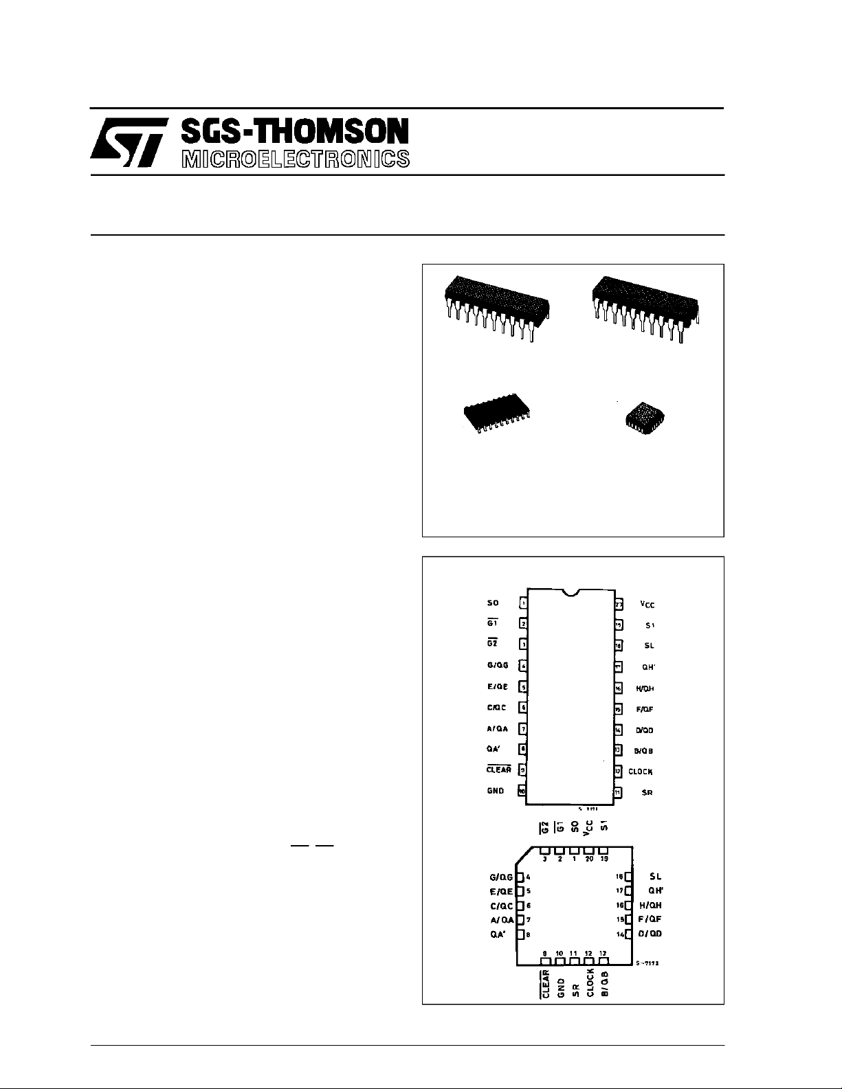
B1R
(PlasticPackage)
F1R
(CeramicPackage)
.SYMMETRICALOUTPUT IMPEDANCE
IOH =IOL= 6mA(MIN.) FORQA,TOQH,
IOH =IOL= 4mA(MIN.) FORQA,TOQ
.BALANCEDPROPAGATION DELAYS
t
PLH=tPHL
.WIDE OPERATING VOLTAGE RANGE
VCC(OPR)= 2 V TO 6 V
.PIN AND FUNCTIONCOMPATIBLE
WITH 54/74LS299
H
M1R
(MicroPackage)
ORDER CODES :
M54HC X XXF 1 R M74H CXXXM1 R
M74HC X XXB1R M74H CXXXC1R
C1R
(Chip Carrier)
DESCRIPTION
The M54/74HC299/323 are high speed CMOS 8BIT PIPO SHIFT REGISTERS (3-STATE) fabricated withsilicon gateC2MOS technology.
They achieve the high speed operation similar to
equivalent LSTTL whilemaintaining the CMOS low
powerconsumption.
These devices have four modes (HOLD, SHIFT
LEFT,SHIFTRIGHTandLOADDATA).Eachmode
is chosen by two function select inputs (S0, S1).
When one orboth enableinputs, (G1, G2)are high,
the eight input/output terminals are in the highimpedance state ; however sequential operation or
clearing of the register is not affected.
Clear function on the HC299 is asynchronous to
CLOCK,while theHC323iscleared synchronous to
clock.
All inputs are equipped with protection circuits
against static discharge and transient excess voltage.
PIN CONNECTIONS(top view)
NC =
No Internal
Connection
October 1993
1/15
Page 2
M54/M74HC299/323
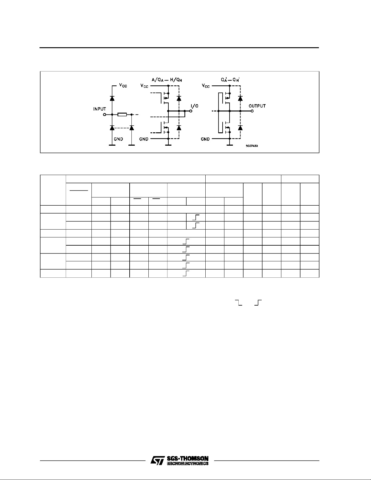
INPUT AND OUTPUT EQUIVALENT CIRCUIT
TRUTH TABLE
INPUTS INPUTS/OUTPUTS OUTPUTS
MODE
CLEAR
FUNCTION
SELECTED
S1 S0 G1 * G2 * (299) (323) SL SR
ZLHHXXXXXZZLL
CLEAR
L LXLLX XXLLLL
L XLLLX XXLLLL
HOLD H L L L L X X X QA0 QH0 QA0 QH0
SHIFT
RIGHT
SHIFT
LEFT
H L H L L X H H QGn H QGn
H L H L L X L L QGn L QGn
H H L L L H X QBn H QBn H
H H L L L L X QBn L QBn L
LOAD H H H X X X X a h a h
* When oneorboth output controls arehigh, theeight, input/outputterminalsareinthehighimpedance state: however sequential operationorclearing
of the registeris not affected.
Z : HIGHIMPEDANCE
Qn0 : THELEVELOF An BEFORE THE INDICATEDSTEADYSTATEINPUT CONDITIONSWERE ESTABLISHED.
Qnn : THELEVELON Qn BEFORETHE MOST RECENTACTIVETRANSITION INDICATEDBY OR
a, h : THELEVEL OFTHE STEADYSTATEINPUTS A, H,RESPECTIVELY.
X : DON’TCARE
OUTPUT
CONTROL
CLOCK SERIAL
A/QA H/QH QA’ QH’
2/15
Page 3
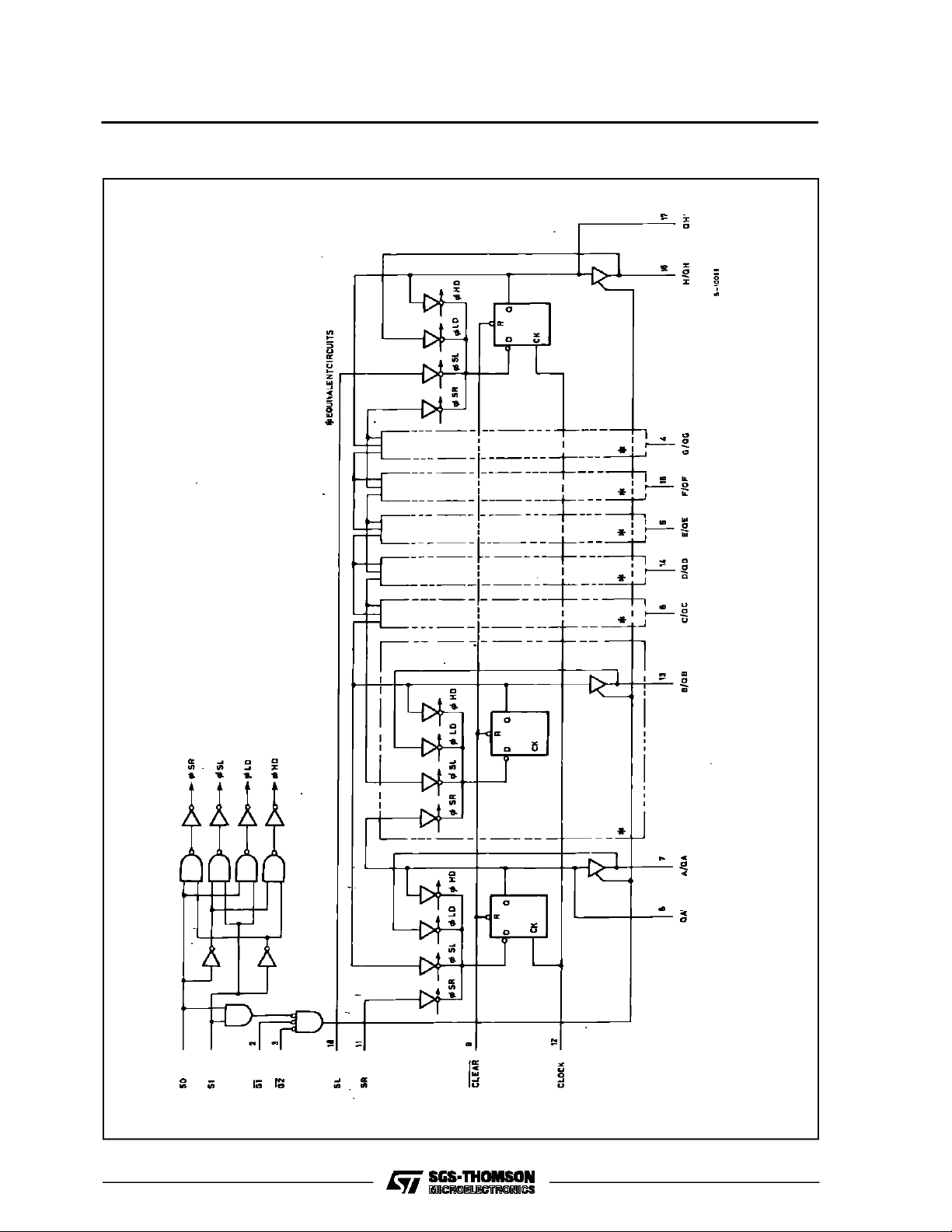
LOGIC DIAGRAM (HC 299)
M54/M74HC299/323
3/15
Page 4
M54/M74HC299/323
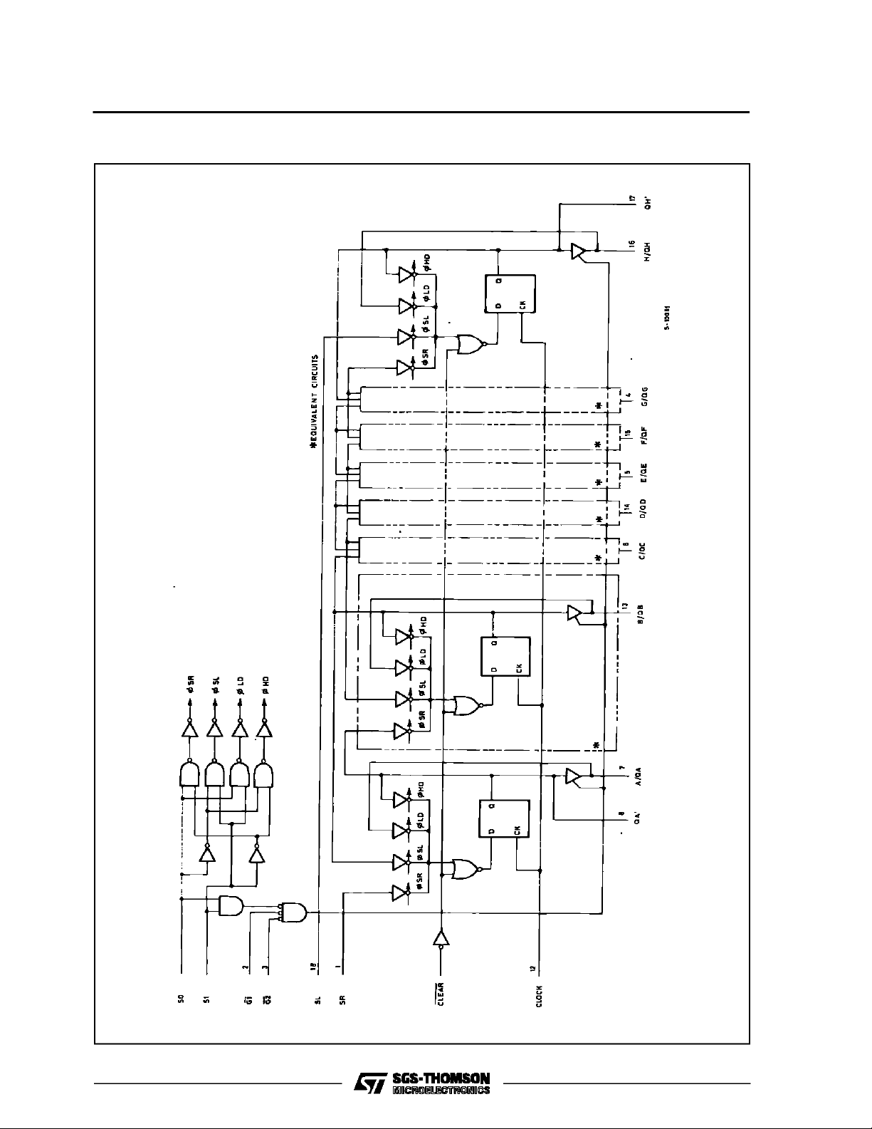
LOGIC DIAGRAM (HC 323)
4/15
Page 5
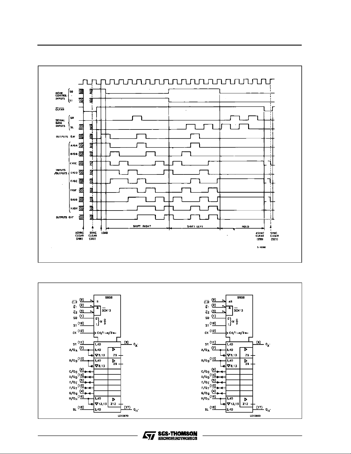
TIMING CHART
M54/M74HC299/323
IEC LOGIC SYMBOLS
HC299 HC299
5/15
Page 6

M54/M74HC299/323
PIN DESCRIPTION
PIN No SYMBOL NAME AND FUNCTION
1, 19 S0, S1 Mode Select Inputs
2, 3 G1, G2 3 State Output Enable Inputs (Active LOW)
7, 13, 6, 14, 5, 15, 4, 16 A/QA to H/QH Parallel Data Inputs or 3 State Parallel Outputs (Bus Driver)
8, 17 QA’ to QH’ Serial Outputs (Standard Output)
9 CLEAR Asynchronous Master Reset Input (Active LOW)
11 SR Serial Data Shift Right Input
12 CLOCK Clock Input (LOWto HIGH, Edge-triggered)
18 SL Serial Data Shift Left Input
10 GND Ground (0V)
20 V
CC
ABSOLU TE M AXI MU M R AT ING S
Symbol Parameter Value Unit
V
CC
V
V
O
I
IK
I
OK
I
O
I
O
I
or I
CC
P
D
T
stg
T
AbsoluteMaximumRatingsarethose valuesbeyondwhichdamage tothedevicemayoccur.Functionaloperationunder theseconditionisnotimplied.
(*)500 mW: ≅ 65oC derateto300 mW by 10mW/oC: 65oCto85oC
Supply Voltage -0.5 to +7 V
DC Input Voltage -0.5 to VCC+ 0.5 V
I
DC Output Voltage -0.5 to VCC+ 0.5 V
DC Input Diode Current ± 20 mA
DC Output Diode Current ± 20 mA
DC Output Source Sink Current Per Output Pin (QA -QH) ± 35 mA
DC OutputSource Sink Current Per Output Pin (QA’ -QH’) ±235 mA
DC VCCor Ground Current ± 70 mA
GND
Power Dissipation 500 (*) mW
Storage Temperature -65 to +150
Lead Temperature (10 sec) 300
L
Positive Supply Voltage
o
C
o
C
RECO MM ENDED OPERAT I N G CO NDI TIONS
Symbol Parameter Value Unit
6/15
V
V
T
t
V
r,tf
Supply Voltage 2 to 6 V
CC
Input Voltage 0 to V
I
Output Voltage 0 to V
O
Operating Temperature: M54HC Series
op
M74HC Series
CC
CC
-55 to +125
-40 to +85
Input Rise and Fall Time VCC= 2 V 0 to 1000 ns
V
= 4.5 V 0 to 500
CC
= 6 V 0 to 400
V
CC
V
V
o
C
o
C
Page 7

DC SPECIFICATIO NS
Symbol Parameter
V
V
V
V
I
I
High Level Input
IH
Voltage
Low Level Input
IL
Voltage
High Level
OH
Output Voltage
QA TO QH 4.5 I
QA’ TO QH’ 4.5 I
Low Level Output
OL
Voltage
QA TO QH 4.5 I
QA’ TO QH’ 4.5 I
I
Input Leakage
I
Current
3 State Output
OZ
Off-state Current
Quiescent Supply
CC
Current
M54/M74HC299/323
Test Conditions Value
=25oC
T
V
(V)
CC
A
54HC and 74HC
Min. Typ. Max. Min. Max. Min. Max.
2.0 1.5 1.5 1.5
4.5 3.15 3.15 3.15
6.0 4.2 4.2 4.2
2.0 0.5 0.5 0.5
4.5 1.35 1.35 1.35
6.0 1.8 1.8 1.8
2.0
V
V
or
V
IO=-20 µA
=
I
IH
=-6.0 mA 4.18 4.31 4.13 4.10
O
IL
=-7.8 mA 5.68 5.8 5.63 5.60
O
=-4.0 mA 4.18 4.31 4.13 4.10
O
=-5.2 mA 5.68 5.8 5.63 5.60
O
4.5 4.4 4.5 4.4 4.4
6.0 5.9 6.0 5.9 5.9
6.0 I
6.0 I
2.0
4.5 0.0 0.1 0.1 0.1
6.0 0.0 0.1 0.1 0.1
6.0 I
6.0 I
6.0
6.0
IO=20µA
V
=
I
V
IH
or
= 6.0 mA 0.17 0.26 0.33 0.40
O
V
IL
= 7.8 mA 0.18 0.26 0.33 0.40
O
= 4.0 mA 0.17 0.26 0.33 0.40
O
= 5.2 mA 0.18 0.26 0.33 0.40
O
VI=VCCor GND ±0.1 ±1 ±1 µA
VI=VIHor V
VO=VCCor GND
1.9 2.0 1.9 1.9
0.0 0.1 0.1 0.1
IL
6.0 VI=VCCor GND 4 40 80 µA
-40 to 85oC
74HC
-55 to 125oC
54HC
Unit
±0.5 ±5 ±10 µA
V
V
V
V
AC ELECTRICAL CHARACTERISTICS (CL=50pF,Inputtr=tf=6ns)
Test Conditions Value
Symbol Parameter
t
t
TLH
THL
Output Transition
Time
(QA, QH)
t
TLH
t
THL
Output Transition
Time
(QA’, QH’)
t
PLH
t
PHL
Propagation
Delay Time
(CK - QA’, QH’)
t
PHL
Propagation
Delay Time
(CLR - QA’, QH’)
=25oC
T
V
C
CC
(V)
L
(pF)
2.0
50
4.5 7121518
A
54HC and 74HC
Min. Typ. Max. Min. Max. Min. Max.
25 60 75 90
6.0 6101315
2.0
50
4.5 8151922
30 75 95 110
6.0 7131619
2.0
50
4.5 23 34 43 51
85 170 215 255
6.0 18 29 37 43
2.0
50 for HC299
4.5 24 35 44 53
85 175 220 265
6.0 18 30 37 45
-40 to 85oC
74HC
-55 to 125oC
54HC
Unit
ns
ns
ns
ns
7/15
Page 8

M54/M74HC299/323
AC ELECTRICAL CHARACTERISTICS (CL=50pF,Inputtr=tf=6ns)
Test Conditions Value
=25oC
T
Symbol Parameter
t
t
PLH
PHL
Propagation
Delay Time
(CK - QA, QH)
V
C
CC
(V)
L
(pF)
2.0
50
4.5 21 32 40 48
6.0 17 27 34 41
2.0
150
4.5 26 40 50 60
A
54HC and 74HC
Min. Typ. Max. Min. Max. Min. Max.
80 160 200 240
100 200 250 300
6.0 21 34 43 51
t
PHL
Propagation
Delay Time
(CLR - QA, QH)
2.0
50 for HC323
4.5 24 38 48 57
85 190 240 285
6.0 18 32 41 48
2.0
150 for HC323
4.5 29 46 58 69
105 230 290 345
6.0 22 39 49 59
t
t
PZL
PZH
3 State Output
Enable Time
2.0
50 R
4.5 17 26 33 39
=1KΩ
L
60 130 165 195
6.0 13 22 28 33
2.0
150 R
4.5 23 34 43 51
=1KΩ
L
78 170 15 255
6.0 17 29 37 43
t
t
PLZ
PHZ
3 State Output
Disable Time
2.0
50 RL=1KΩ
4.5 19 30 38 45
54 150 190 225
6.0 16 26 32 38
f
MAX
Maximum Clock
Frequency
2.0
50
4.5 30 58 24 20
6 12 4.8 4
6.0 35 80 28 24
t
W(L)
t
W(H)
t
W(L)
t
REM
C
C
PD
Minimum Pulse
Width
(CLOCK)
Minimum Pulse
Width
(CLEAR)
t
Minimum Set-up
s
Time (S0, S1)
(SL, SR, A H)
(CLEAR for 323)
Minimum Hold
t
h
Time (S0, S1)
(SL, SR, A H)
(CLEAR for 323)
Minimum
Removal Time
(CLEAR)
Input Capacitance 5 10 10 10 pF
IN
(*) Power Dissipation
2.0
50
4.5 15 19 22
6.0 13 16 19
2.0
50 for HC299
4.5 15 19 22
6.0 13 16 19
2.0
4.5 20 25 30
50
6.0 17 21 26
2.0
4.5 0 0 0
50
6.0 0 0 0
2.0
50 for HC299
4.5 10 13 15
6.0 9 11 13
170
Capacitance
(*) CPDisdefined as the valueofthe IC’s internal equivalent capacitance which is calculated from the operatingcurrent consumption without load.
(Referto Test Circuit).Average operting current can be obtained bythe followingequation. ICC(opr) = CPD•VCC•fIN+I
-40 to 85oC
74HC
-55 to 125oC
54HC
Unit
ns
ns
ns
ns
ns
ns
ns
ns
75 95 110
ns
75 95 110
ns
100 125 150
ns
000
ns
50 65 75
ns
pF
CC
8/15
Page 9

SWITCHING CHARACTERISTICS TEST WAVEFORM
HC299
M54/M74HC299/323
HC323
9/15
Page 10

M54/M74HC299/323
TEST CIRCUIT ICC(Opr.)
10/15
Page 11

Plastic DIP20 (0.25) MECHANICAL DATA
M54/M74HC299/323
DIM.
MIN. TYP. MAX. MIN. TYP. MAX.
a1 0.254 0.010
B 1.39 1.65 0.055 0.065
b 0.45 0.018
b1 0.25 0.010
D 25.4 1.000
E 8.5 0.335
e 2.54 0.100
e3 22.86 0.900
F 7.1 0.280
I 3.93 0.155
L 3.3 0.130
Z 1.34 0.053
mm inch
P001J
11/15
Page 12

M54/M74HC299/323
Ceramic DIP20 MECHANICAL DATA
DIM.
MIN. TYP. MAX. MIN. TYP. MAX.
A 25 0.984
B 7.8 0.307
D 3.3 0.130
E 0.5 1.78 0.020 0.070
e3 22.86 0.900
F 2.29 2.79 0.090 0.110
G 0.4 0.55 0.016 0.022
I 1.27 1.52 0.050 0.060
L 0.22 0.31 0.009 0.012
M 0.51 1.27 0.020 0.050
N1 4° (min.), 15° (max.)
P 7.9 8.13 0.311 0.320
Q 5.71 0.225
mm inch
12/15
P057H
Page 13

SO20 MECHANICAL DATA
M54/M74HC299/323
DIM.
MIN. TYP. MAX. MIN. TYP. MAX.
A 2.65 0.104
a1 0.10 0.20 0.004 0.007
a2 2.45 0.096
b 0.35 0.49 0.013 0.019
b1 0.23 0.32 0.009 0.012
C 0.50 0.020
c1 45° (typ.)
D 12.60 13.00 0.496 0.512
E 10.00 10.65 0.393 0.419
e 1.27 0.050
e3 11.43 0.450
F 7.40 7.60 0.291 0.299
L 0.50 1.27 0.19 0.050
M 0.75 0.029
S8°(max.)
mm inch
P013L
13/15
Page 14

M54/M74HC299/323
PLCC20 MECHANICAL DATA
DIM.
MIN. TYP. MAX. MIN. TYP. MAX.
A 9.78 10.03 0.385 0.395
B 8.89 9.04 0.350 0.356
D 4.2 4.57 0.165 0.180
d1 2.54 0.100
d2 0.56 0.022
E 7.37 8.38 0.290 0.330
e 1.27 0.050
e3 5.08 0.200
F 0.38 0.015
G 0.101 0.004
M 1.27 0.050
M1 1.14 0.045
mm inch
14/15
P027A
Page 15

M54/M74HC299/323
Information furnishedis believed to be accurate and reliable. However, SGS-THOMSON Microelectronics assumesno responsability for the
consequences of useof such information norfor anyinfringement of patents orother rightsof third parties whichmay results from its use.No
license is granted byimplication or otherwiseunderany patent orpatent rights ofSGS-THOMSON Microelectronics. Specificationsmentioned
in thispublication are subject to changewithout notice.This publicationsupersedes and replacesall information previously supplied.
SGS-THOMSON Microelectronicsproducts are not authorized foruse ascritical componentsin life supportdevicesorsystemswithoutexpress
written approval ofSGS-THOMSON Microelectonics.
1994SGS-THOMSON Microelectronics- All RightsReserved
Australia -Brazil - France - Germany - Hong Kong - Italy -Japan - Korea -Malaysia - Malta - Morocco- The Netherlands -
Singapore -Spain - Sweden - Switzerland - Taiwan - Thailand - United Kingdom -U.S.A
SGS-THOMSON Microelectronics GROUP OFCOMPANIES
15/15
 Loading...