

Datasheet M74HC30TTR, M74HC30RM13TR, M74HC30M1R, M74HC30B1R Datasheet (SGS Thomson Microelectronics)
Page 1
M74HC30
8-INPUT NAND GATE
■ HIGH SPEED:
t
= 13ns (TYP.) at VCC = 6V
PD
■ LOW POWER DISSIPATION:
I
= 1µA(MAX.) at TA=25°C
CC
■ HIGH NOISE IMMUNITY:
V
= V
NIH
■ SYMMETRICAL OUTPUT IMPEDANCE:
|I
| = IOL = 4mA (MIN)
OH
■ BALANCED PROPAGATION DELAYS:
t
≅ t
PLH
■ WIDE OPERATING VOLTAGE RANGE:
V
(OPR) = 2V to 6V
CC
■ PIN AND FUNCTION COMPATIBLE WITH
= 28 % VCC (MIN.)
NIL
PHL
74 SERIES 30
DESCRIPTION
The M74HC30 is an high speed CMOS 8-INPUT
NAND GATE fabricated with silicon gate C
2
MOS
technology.
The internal circuit is composed of 5 stages
including buffer output , which enables high noise
immunity and stable output.
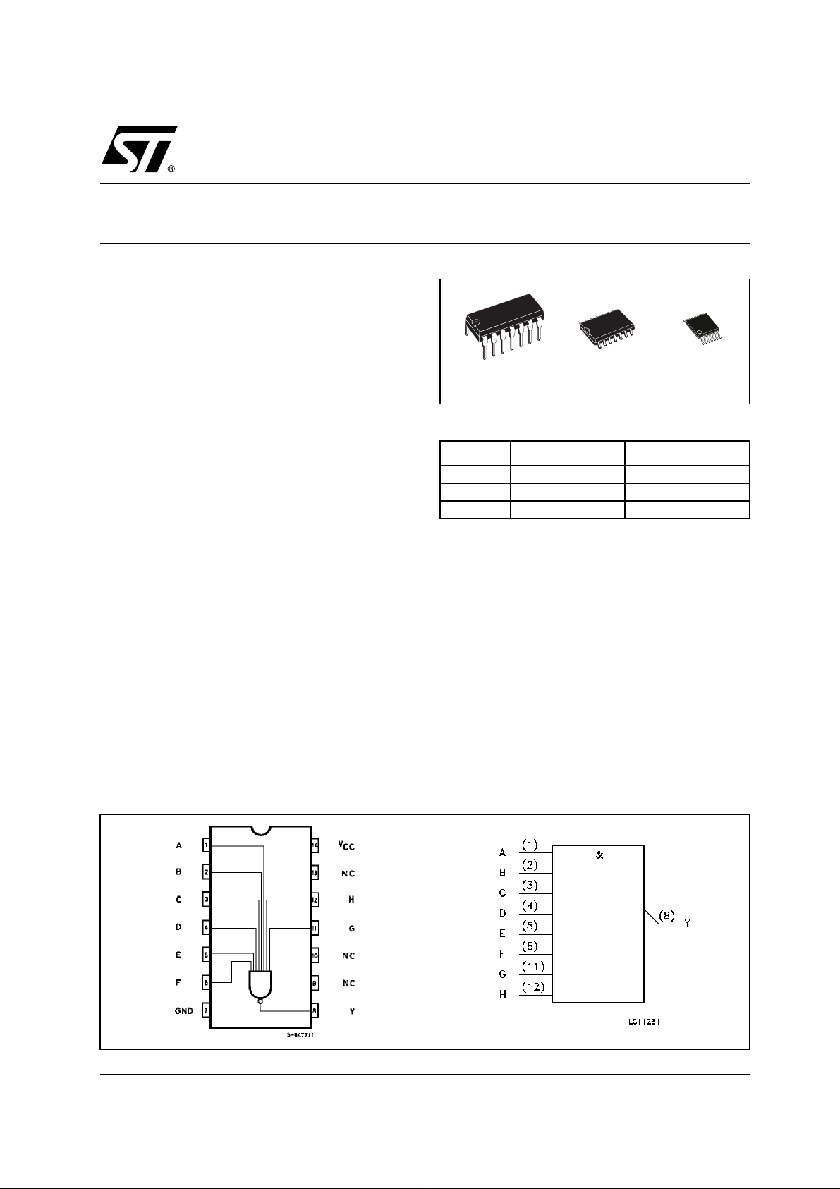
TSSOPDIP SOP
ORDER CODES
PACKAGE TUBE T & R
DIP M74HC30B1R
SOP M74HC30M1R M74HC30RM13TR
TSSOP M74HC30TTR
All inputs are equipped with protection circuits
against static discharge and transient excess
voltage.
PIN CONNECTION AND IEC LOGIC SYMBOLS
1/8July 2001
Page 2
M74HC30
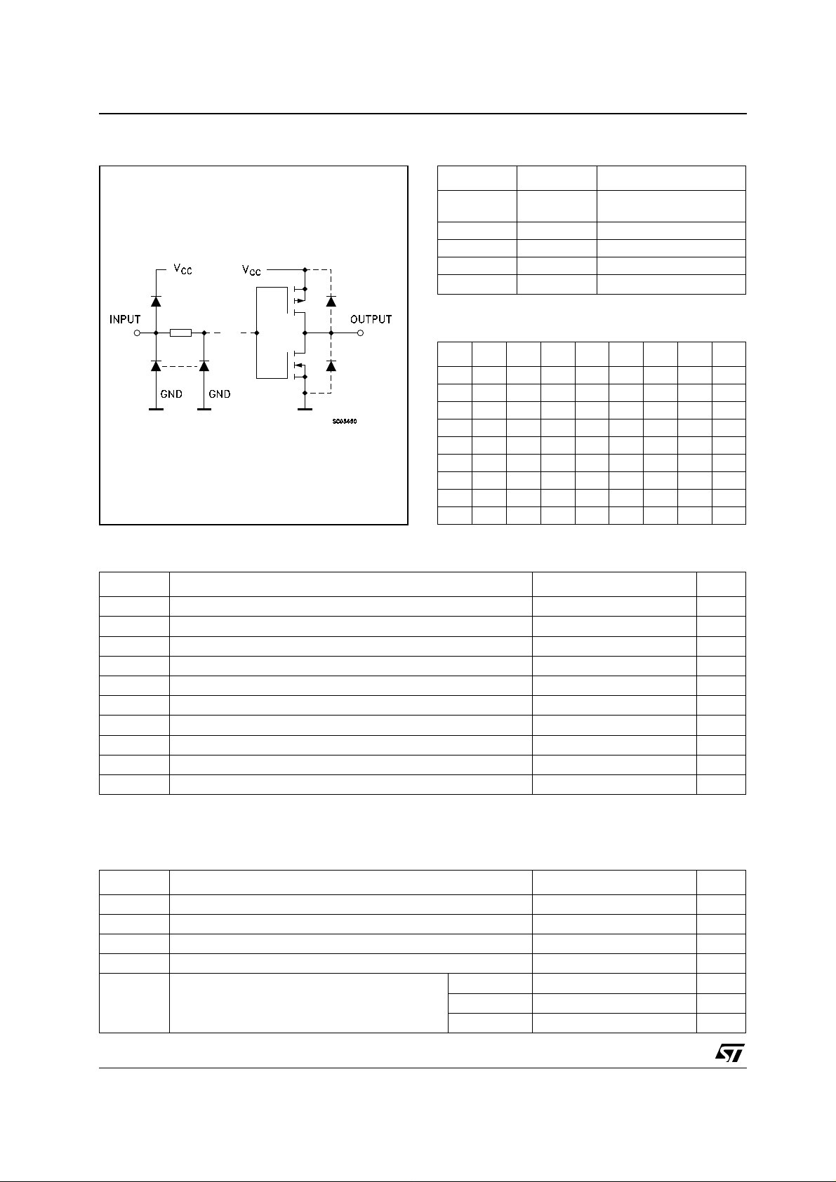
INPUT AND OUTPUT EQUIVALENT CIRCUIT PIN DESCRIPTION
PIN No SYMBOL NAME AND FUNCTION
1, 2, 3 ,4, 5,
6, 11, 12
9, 10, 13 NC Not connected
8 Y Data Output
7 GND Ground (0V)
14
TRUTH TABLE
ABCDEFGHY
LXXXXXXXH
XLXXXXXXH
XXLXXXXXH
XXXLXXXXH
XXXXLXXXH
XXXXXLXXH
XXXXXXLXH
XXXXXXXLH
HHHHHHHHL
A, B, C, D, E,
F, G, H,
V
CC
Data Inputs
Positive Supply Voltage
ABSOLUTE MAXIMUM RATINGS
Symbol Parameter Value Unit
V
V
V
I
I
OK
I
I
or I
CC
P
T
T
Absolute Maximum Ratings are those values beyond which damage to the device may occur. Functional operation under these conditions is
not implied
(*) 500mW at 65
Supply Voltage
CC
DC Input Voltage -0.5 to VCC + 0.5
I
DC Output Voltage -0.5 to VCC + 0.5
O
DC Input Diode Current
IK
DC Output Diode Current
DC Output Current
O
DC VCC or Ground Current
GND
Power Dissipation
D
Storage Temperature
stg
Lead Temperature (10 sec)
L
°C; derate to 300mW by 10mW/°C from 65°C to 85°C
-0.5 to +7 V
V
V
± 20 mA
± 20 mA
± 25 mA
± 50 mA
500(*) mW
-65 to +150 °C
300 °C
RECOMMENDED OPERATING CONDITIONS
Symbol Parameter Value Unit
V
V
V
T
t
r
Supply Voltage
CC
Input Voltage 0 to V
I
Output Voltage 0 to V
O
Operating Temperature
op
Input Rise and Fall Time VCC = 2.0V
, t
f
V
V
CC
CC
= 4.5V
= 6.0V
2 to 6 V
CC
CC
-55 to 125 °C
0 to 1000 ns
0 to 500 ns
0 to 400 ns
V
V
2/8
Page 3
DC SPECIFICATIONS
Symbol P arameter
V
V
V
V
I
High Level Input
IH
Voltage
Low Level Input
IL
Voltage
High Level Output
OH
Voltage
Low Level Output
OL
Voltage
I
Input Leakage
I
Current
Quiescent Supply
CC
Current
M74HC30
Test Condition Value
T
= 25°C
V
CC
(V)
A
Min. Typ. Max. Min. Max. Min. Max.
2.0 1.5 1.5 1.5
6.0 4.2 4.2 4.2
2.0 0.5 0.5 0.5
6.0 1.8 1.8 1.8
2.0
4.5
6.0
4.5
6.0
2.0
4.5
6.0
4.5
6.0
6.0
6.0
IO=-20 µA
I
=-20 µA
O
I
=-20 µA
O
I
=-4.0 mA
O
I
=-5.2 mA
O
IO=20 µA
I
=20 µA
O
I
=20 µA
O
I
=4.0 mA
O
I
=5.2 mA
O
= VCC or GND
V
I
= VCC or GND
V
I
1.9 2.0 1.9 1.9
4.4 4.5 4.4 4.4
5.9 6.0 5.9 5.9
4.18 4.31 4.13 4.10
5.68 5.8 5.63 5.60
0.0 0.1 0.1 0.1
0.0 0.1 0.1 0.1
0.0 0.1 0.1 0.1
0.17 0.26 0.33 0.40
0.18 0.26 0.33 0.40
-40 to 85°C -55 to 125°C
± 0.1 ± 1 ± 1 µA
11020µA
Unit
V4.5 3.15 3.15 3.15
V4.5 1.35 1.35 1.35
V
V
AC ELECTRICAL CHARACTERISTICS (C
= 50 pF, Input tr = tf = 6ns)
L
Test Condition Value
T
Symbol Parameter
t
TLH tTHL
Output Transition
Time
V
CC
(V)
2.0 30 75 95 110
= 25°C
A
-40 to 85°C -55 to 125°C
Min. Typ. Max. Min. Max. Min. Max.
Unit
ns4.5 8151922
6.0 7131619
t
PLH tPHL
Propagation Delay
Time
2.0 45 115 145 170
ns4.5 15 23 29 34
6.0 13 20 25 29
CAPACITIVE CHARACTERISTICS
Test Condition Value
T
Symbol Parameter
V
CC
(V)
C
C
1) CPD is defined as the value of the IC’s internal equivalent capacitance which is calculated from the operating current consumption without
load. (R ef er to Test Circui t). Averag e operating current can be obtained by the following equation. I
Input Capacitance
IN
Power Dissipation
PD
Capacitance (note 1)5.0 20 pF
5.0 5101010pF
= 25°C
A
Min. Typ. Max. Min. Max. Min. Max.
-40 to 85°C -55 to 125°C
= CPD x VCC x fIN + I
CC(opr)
CC
Unit
3/8
Page 4
M74HC30
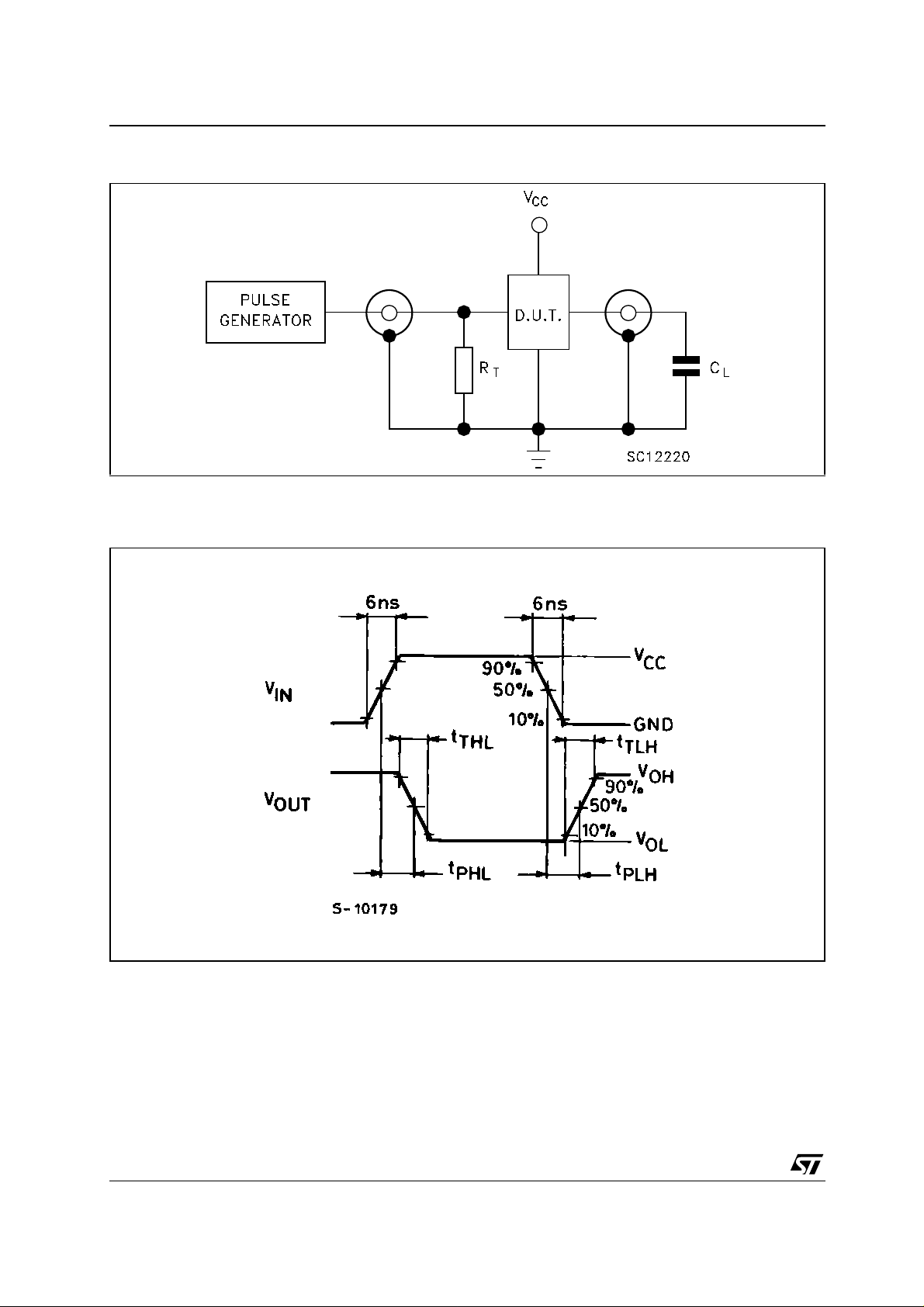
TEST CIRCUIT
CL = 50pF or equivalent (includes jig and p robe capacit ance)
R
= Z
of pulse generator (typically 50Ω)
T
OUT
WAVEFORM : PROPAGATION DELAY TIMES (f=1MHz; 50% duty cycle)
4/8
Page 5

M74HC30
Plastic DIP-14 MECHANICAL DATA
mm. inch
DIM.
MIN. TYP MAX. MIN. TYP. MAX.
a1 0.51 0.020
B 1.39 1.65 0.055 0.065
b 0.5 0.020
b1 0.25 0.010
D 20 0.787
E 8.5 0.335
e 2.54 0.100
e3 15.24 0.600
F 7.1 0.280
I 5.1 0.201
L 3.3 0.130
Z 1.27 2.54 0.050 0.100
P001A
5/8
Page 6

M74HC30
SO-14 MECHANICAL DATA
DIM.
A 1.75 0.068
a1 0.1 0.2 0.003 0.007
a2 1.65 0.064
b 0.35 0.46 0.013 0.018
b1 0.19 0.25 0.007 0.010
C 0.5 0.019
c1 45° (typ.)
D 8.55 8.75 0.336 0.344
E 5.8 6.2 0.228 0.244
e 1.27 0.050
e3 7.62 0.300
F 3.8 4.0 0.149 0.157
G 4.6 5.3 0.181 0.208
L 0.5 1.27 0.019 0.050
M 0.68 0.026
S8° (max.)
MIN. TYP MAX. MIN. TYP. M AX.
mm. inch
6/8
PO13G
Page 7
M74HC30
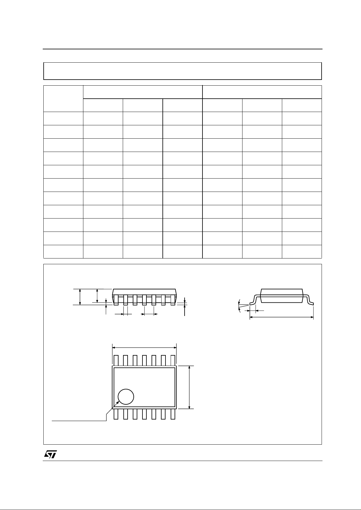
TSSOP14 MECHANICAL DATA
mm. inch
DIM.
MIN. TYP MAX. MIN. TYP. M AX.
A 1.2 0.047
A1 0.05 0.15 0.002 0.004 0.006
A2 0.8 1 1.05 0.031 0.039 0.041
b 0.19 0.30 0.007 0.012
c 0.09 0.20 0.004 0.0089
D 4.9 5 5.1 0.193 0.197 0.201
E 6.2 6.4 6.6 0.244 0.252 0.260
E1 4.3 4.4 4.48 0.169 0.173 0.176
e 0.65 BSC 0.0256 BSC
K0° 8°0° 8°
L 0.45 0.60 0.75 0.018 0.024 0.030
A2
A
A1
b
e
c
K
L
E
D
E1
PIN 1 IDENTIFICATION
1
0080337D
7/8
Page 8

M74HC30
Information furnished is bel ieved to be accurate and reliable. However, STMicroe lectronics assumes no responsibility for the
consequences of use of such information nor for any infringement of patents or other rights of third parties which may result from
its use. No li cense is granted by imp lication or otherwise under a ny patent or patent rig hts of STMicroelectronics. Spec ific at ions
mentioned in this publication ar e subject to change without notice. This publication supersedes and replaces all information
previously supplied. S TMicroelectronics products are not authorized for use as critica l components in life suppo rt devices or
systems without express written approval of STMicroelectronics.
Australi a - Brazil - Chi na - Finland - F rance - Germany - Hong Kon g - I ndia - Italy - Japan - Malay sia - Malta - Morocco
© The ST logo is a registered trademark of STMicroelectronics
© 2001 STM icroelectronics - Printed in Ital y - All Rights Reserved
STMicr o el ectronics GROUP OF COMPANIES
Singapo re - Spain - Sweden - Switzerland - Uni ted Kingdom
© http://www.st.com
8/8
 Loading...