

Page 1
QUAD 2 CHANNEL MULTIPLEXER/REGISTER
.HIGH SPEED
f
= 73 MHz(typ.) AT VCC=5V
MAX
.LOWPOWERDISSIPATION
ICC=4µA(MAX.) AT TA=25°C
.HIGH NOISEIMMUNITY
V
NIH=VNIL
=28%VCC(MIN.)
.OUTPUT DRIVE CAPABILITY
10 LSTTL LOADS
.SYMMETRICALOUTPUT IMPEDANCE
IOH =IOL= 4 mA(MIN.)
.BALANCEDPROPAGATION DELAYS
t
PLH=tPHL
.WIDE OPERATINGVOLTAGE RANGE
VCC(OPR)= 2V TO6 V
.PIN ANDFUNCTION COMPATIBLE
WITH 54/74LS298
DESCRIPTION
The M54/74HC298 isahighspeedCMOSQUAD2CHANNEL MULTIPLEXER/REGISTER fabricated
in silicongate C2MOStechnology.
It has the same high speed performance of LSTTL
combined withtrue CMOSlowpower consumption.
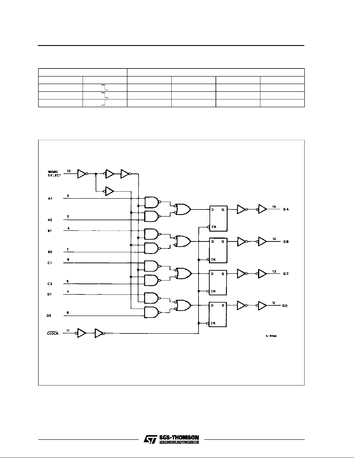
Thesecircuits are controlled by the signals WORD
SELECT and CLOCK. When the WORD SELECT
input is taken low Word 1 (A1, B1, C1 and D1) is
presented to the input of the flip-flops, and when
WORDSELECT ishighWord 2(A2,B2,C2 and D2)
is presented to theinputs of theflip-flops. Theselect
wordis clockedtothe outputterminals onthe negative edge oftheclockpulse. Allinputsare equipped
with protection circuitsagainst static discharge and
transient excess voltage.
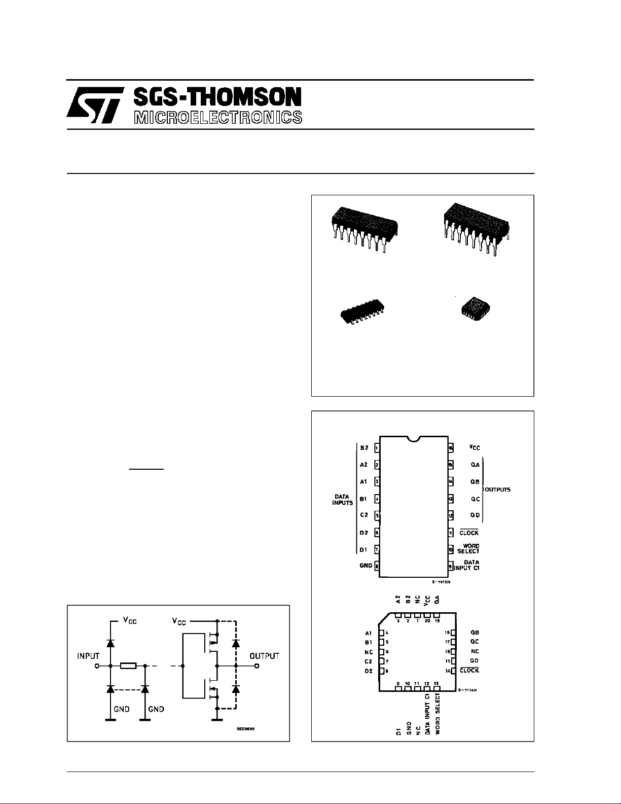
M54HC298
M74HC298
B1R
(PlasticPackage)
M1R
(MicroPackage)
ORDER CODES :
M54HC 298F1R M74H C298M1R
M74HC 298B1R M74HC2 98C1R
PIN CONNECTIONS(top view)
F1R
(CeramicPackage)
C1R
(Chip Carrier)
INPUT AND OUTPUT EQUIVALENT CIRCUIT
October 1992
NC =
No Internal
Connection
1/11
Page 2
M54/M74HC298
TRUTH TABLE
INPUTS OUTPUTS
WORD SELECT CLOCK QA QB QC QD
La1b1c1d1
Ha2b2c2d2
X : DON’T CARE(INCLUDINGTRANSITION)
a1, a2, ETC : THE LEVELOF STEAY STATEINPUT ATa1, a2,etc.
QA0, QB0,ETC: THE LEVEL OF QA, QB,ETC ENTEREDON THE MOSTRECENT NEGATIVETRANSITION OF THECLOCK INPUT.
LOGI C DI AGRAM
X QA0 QB0 QC0 QD0
2/11
Page 3
M54/M74HC298
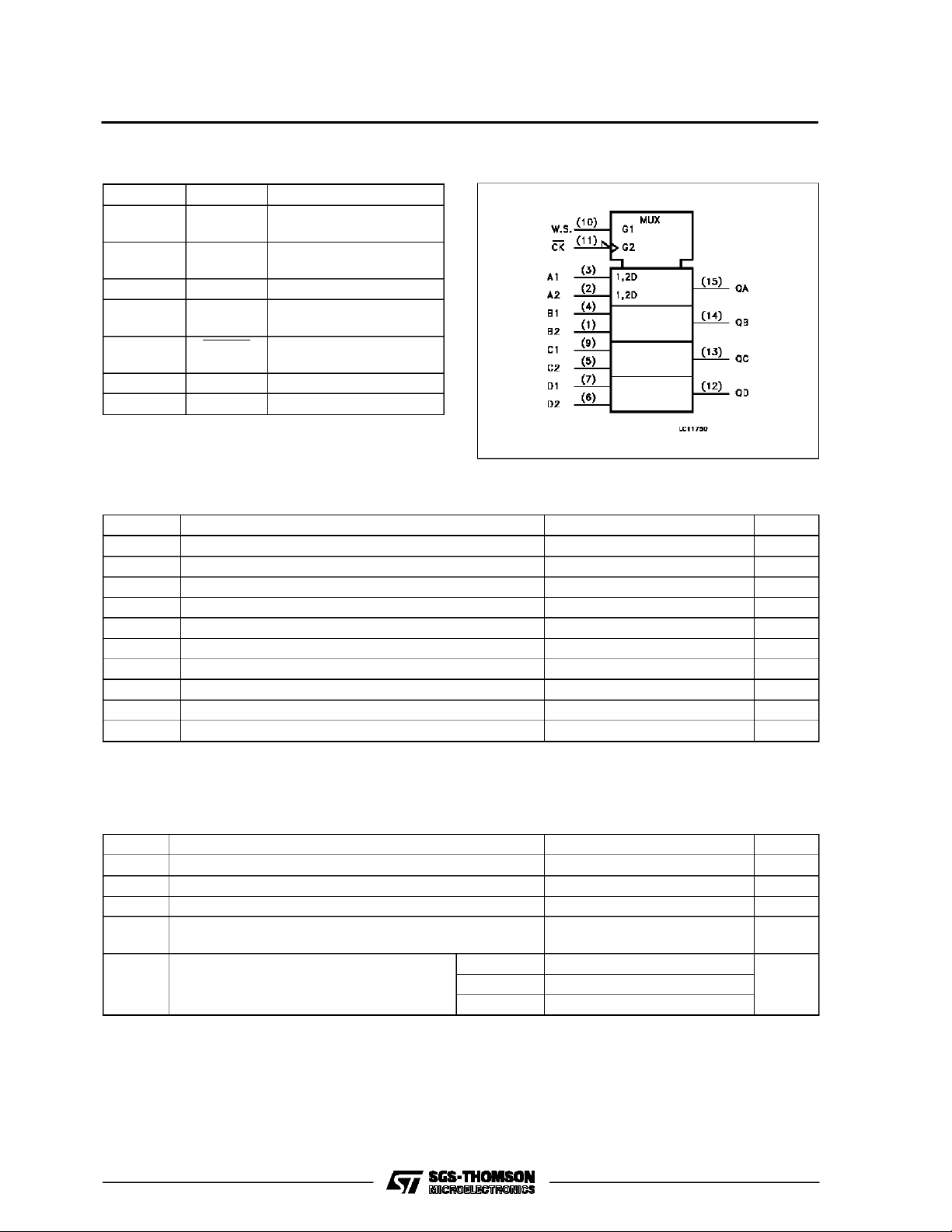
PIN DESC RIPTION
IEC LOGIC SYMBOL
PIN No SYMBOL NAME AND FUNCTION
1, 2, 5, 6 A2, B2,
Word 2 Data Inputs
C2, D2
3, 4, 7, 9 A1, B1,
Word 1 Data Inputs
C1, D1
12 to 15 QA to QD Outputs
10 WORD
Word Select Input
SELECT
11 CLOCK Clock Input (HIGH to
LOW, Edge-triggered)
8 GND Ground (0V)
16 V
CC
Positive Supply Voltage
ABSOLU TE M AXIMU M R AT INGS
Symbol Parameter Value Unit
V
CC
V
V
O
I
IK
I
OK
I
O
or I
I
CC
P
D
T
stg
T
AbsoluteMaximumRatingsarethose valuesbeyond whichdamage to thedevice mayoccur.Functional operation under these conditionisnotimplied.
(*)500 mW: ≅ 65oC derateto300 mWby 10mW/oC: 65oCto85oC
Supply Voltage -0.5 to +7 V
DC Input Voltage -0.5 to VCC+ 0.5 V
I
DC Output Voltage -0.5 to VCC+ 0.5 V
DC Input Diode Current ± 20 mA
DC Output Diode Current ± 20 mA
DC Output Source Sink Current Per Output Pin ± 25 mA
DC VCCor Ground Current ± 50 mA
GND
Power Dissipation 500 (*) mW
Storage Temperature -65 to +150
Lead Temperature (10sec) 300
L
o
C
o
C
RECO MM ENDED OPERATI N G CO NDI TIONS
Symbol Parameter Value Unit
V
V
T
t
V
r,tf
Supply Voltage 2 to 6 V
CC
Input Voltage 0 to V
I
Output Voltage 0 to V
O
Operating Temperature: M54HC Series
op
M74HC Series
CC
CC
-55 to +125
-40 to +85
Input Rise and Fall Time VCC= 2 V 0 to 1000 ns
V
= 4.5 V 0 to 500
CC
= 6 V 0 to 400
V
CC
V
V
o
C
o
C
3/11
Page 4
M54/M74HC298
DC SPECIFICATIONS
Symbol Parameter
V
V
V
V
I
High Level Input
IH
Voltage
Low Level Input
IL
Voltage
High Level
OH
Output Voltage
Low Level Output
OL
Voltage
I
Input Leakage
I
Current
Quiescent Supply
CC
Current
Test Conditions Value
V
(V)
CC
=25oC
A
54HC and 74HC
Min. Typ. Max. Min. Max. Min. Max.
-40 to 85oC
74HC
-55 to 125oC
54HC
Unit
T
2.0 1.5 1.5 1.5
4.5 3.15 3.15 3.15
6.0 4.2 4.2 4.2
2.0 0.5 0.5 0.5
4.5 1.35 1.35 1.35
6.0 1.8 1.8 1.8
2.0
4.5 4.4 4.5 4.4 4.4
6.0 5.9 6.0 5.9 5.9
4.5 I
6.0 I
2.0
4.5 0.0 0.1 0.1 0.1
6.0 0.0 0.1 0.1 0.1
4.5 I
6.0 I
6.0
=
V
I
IO=-20 µA
V
IH
or
V
IL
=-4.0 mA 4.18 4.31 4.13 4.10
O
=-5.2 mA 5.68 5.8 5.63 5.60
O
V
=
I
IO=20µA
V
IH
or
V
IL
= 4.0 mA 0.17 0.26 0.33 0.40
O
= 5.2 mA 0.18 0.26 0.33 0.40
O
VI=VCCor GND ±0.1 ±1 ±1 µA
1.9 2.0 1.9 1.9
0.0 0.1 0.1 0.1
6.0 VI=VCCor GND 4 40 80 µA
V
V
V
V
4/11
Page 5

M54/M74HC298
AC ELECTRICAL CHARACTERISTICS (CL=50pF,Inputtr=tf=6ns)
Test Conditions Value
T
=25oC
Symbol Parameter
t
t
TLH
THL
Output Transition
Time
V
CC
(V)
2.0 30 75 95 110
4.5 8151922
A
54HC and 74HC
Min. Typ. Max. Min. Max. Min. Max.
6.0 7131619
t
PLH
t
PHL
f
MAX
Propagation
Delay Time
(CLOCK - Q)
Maximum Clock
Frequency
2.0 45 125 155 190
4.5 15 25 31 38
6.0 13 21 26 32
2.0 7 22 5.6 4.6
4.5 35 67 28 23
6.0 41 79 33 25
t
W(H)
t
W(L)
Minimum Pulse
Width
(CLOCK)
Minimum Set-up
t
s
Time
(A, B, C, D)
t
Minimum Set-up
s
Time
(W. S.)
Minimum Hold
t
h
Time
(A, B, C, D)
Minimum Hold
t
h
Time
(W. S.)
C
C
PD
Input Capacitance 5 10 10 10 pF
IN
(*) Power Dissipation
2.0 18 75 95 110
4.5 6151922
6.0 6131619
2.0 12 50 65 75
4.5 3101315
6.0 2 9 11 13
2.0 30 75 95 110
4.5 8151922
6.0 6131619
2.0 25 30 40
4.5 5 6 8
6.0 4 5 7
2.0 0 0 0
4.5 0 0 0
6.0 0 0 0
39
Capacitance
(*) CPDisdefined as the value ofthe IC’sinternal equivalent capacitance which is calculated fromthe operatingcurrent consumption without load.
(Referto Test Circuit).Average operting currentcanbe obtained by the followingequation.ICC(opr) = CPD•VCC•fIN+ICC/4 (perbit),and theCPDfor
operating current can be obtained by the following equation: CPD= 27 +12 xn
-40 to 85oC
74HC
-55 to 125oC
54HC
Unit
ns
ns
MHz
ns
ns
ns
ns
ns
pF
5/11
Page 6

M54/M74HC298
SWITCHING CHARACTERISTICS TEST WAVEFORM
TEST CIRCUIT
TRANSITIONTIME AND VIH,VILOFINPUTWAVEFORMIS THE SAMEAS THATIN CASEOFSWITCHINGCHARACTERISTICSTEST.
6/11
Page 7

Plastic DIP16 (0.25) MECHANICAL DATA
M54/M74HC298
DIM.
MIN. TYP. MAX. MIN. TYP. MAX.
a1 0.51 0.020
B 0.77 1.65 0.030 0.065
b 0.5 0.020
b1 0.25 0.010
D 20 0.787
E 8.5 0.335
e 2.54 0.100
e3 17.78 0.700
F 7.1 0.280
I 5.1 0.201
L 3.3 0.130
Z 1.27 0.050
mm inch
P001C
7/11
Page 8

M54/M74HC298
Ceramic DIP16/1 MECHANICAL DATA
DIM.
MIN. TYP. MAX. MIN. TYP. MAX.
A 20 0.787
B 7 0.276
D 3.3 0.130
E 0.38 0.015
e3 17.78 0.700
F 2.29 2.79 0.090 0.110
G 0.4 0.55 0.016 0.022
H 1.17 1.52 0.046 0.060
L 0.22 0.31 0.009 0.012
M 0.51 1.27 0.020 0.050
N 10.3 0.406
P 7.8 8.05 0.307 0.317
Q 5.08 0.200
mm inch
8/11
P053D
Page 9

SO16 (Narrow) MECHANICAL DATA
M54/M74HC298
DIM.
MIN. TYP. MAX. MIN. TYP. MAX.
A 1.75 0.068
a1 0.1 0.2 0.004 0.007
a2 1.65 0.064
b 0.35 0.46 0.013 0.018
b1 0.19 0.25 0.007 0.010
C 0.5 0.019
c1 45° (typ.)
D 9.8 10 0.385 0.393
E 5.8 6.2 0.228 0.244
e 1.27 0.050
e3 8.89 0.350
F 3.8 4.0 0.149 0.157
G 4.6 5.3 0.181 0.208
L 0.5 1.27 0.019 0.050
M 0.62 0.024
S8°(max.)
mm inch
P013H
9/11
Page 10

M54/M74HC298
PLCC20 MECHANICAL DATA
DIM.
MIN. TYP. MAX. MIN. TYP. MAX.
A 9.78 10.03 0.385 0.395
B 8.89 9.04 0.350 0.356
D 4.2 4.57 0.165 0.180
d1 2.54 0.100
d2 0.56 0.022
E 7.37 8.38 0.290 0.330
e 1.27 0.050
e3 5.08 0.200
F 0.38 0.015
G 0.101 0.004
M 1.27 0.050
M1 1.14 0.045
mm inch
10/11
P027A
Page 11

M54/M74HC298
Information furnishedis believed to be accurate and reliable. However, SGS-THOMSON Microelectronicsassumes no responsability for the
consequences of useof suchinformation nor for any infringement of patents or other rights of third parties which may results from its use. No
license is granted byimplication or otherwiseunder any patentor patentrights ofSGS-THOMSON Microelectronics.Specificationsmentioned
in this publication are subjectto changewithout notice. This publication supersedes andreplaces all information previouslysupplied.
SGS-THOMSON Microelectronicsproducts are not authorized foruse ascritical componentsin life supportdevices or systems without express
written approval of SGS-THOMSON Microelectonics.
1994SGS-THOMSON Microelectronics- All Rights Reserved
Australia -Brazil - France - Germany - Hong Kong - Italy - Japan - Korea - Malaysia - Malta -Morocco - The Netherlands-
Singapore -Spain - Sweden- Switzerland - Taiwan - Thailand- UnitedKingdom - U.S.A
SGS-THOMSON Microelectronics GROUP OFCOMPANIES
11/11
 Loading...