

Page 1
QUAD BUS TRANSCEIVER (3-STATE)
.HIGH SPEED
tPD= 9 ns (TYP.)AT VCC=5V
.LOWPOWERDISSIPATION
ICC=4µA(MAX.) AT 25 °C
.OUTPUT DRIVE CAPABILITY
15 LSTTL LOADS
.BALANCEDPROPAGATION DELAYS
t
PLH=tPHL
.SYMMETRICALOUTPUT IMPEDANCE
IOL=IOH = 6 mA (MIN.)
.HIGH NOISE IMMUNITY
V
NIH=VNIL
=28%VCC(MIN.)
.WIDE OPERATINGVOLTAGE RANGE
VCC(OPR)= 2V TO6 V
.PIN ANDFUNCTION COMPATIBLE
WITH 54/74LS242/243
DESCRIPTION
The M54/74HC242/243 are high speed CMOS
QUAD BUS TRANSCEIVER (3-STATE)
FABRICATED IN SILICON GATE C2MOS
technology. They have the same high speed
performance of LSTTL combined with true CMOS
low power consumption. The HC242/243 are 3
STATE bi-directional inverting and non-inverting
buffersand are intendedfor two-wayasynchronous
communication betweendata buses. They arehigh
drive current outputs which enable high speed
operation when driving large bus capacitances.
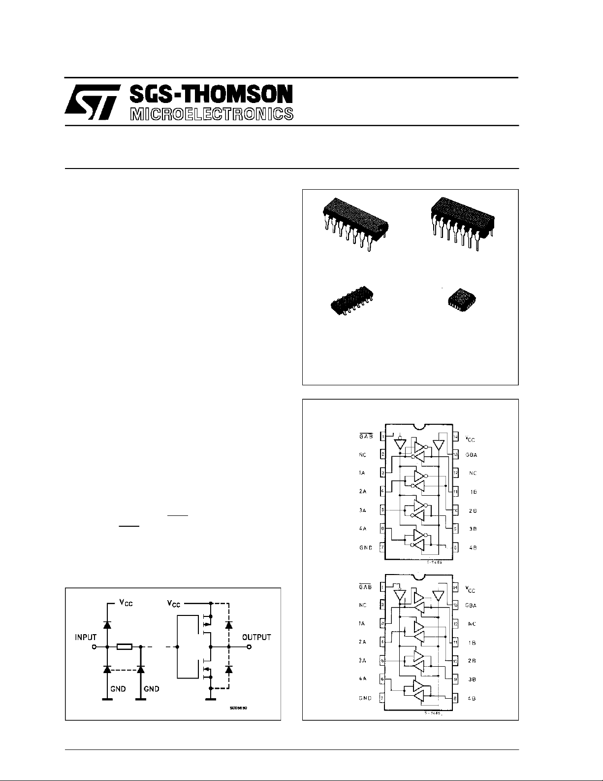
Eachdevice hasone activehighenable (GBA),and
one active low enable (GAB). GBA enables the A
outputs and GAB enables the B outputs. All inputs
are equipped with protection circuits against static
discharge and transient excess voltage.
M54/74HC242
M54/74HC243
B1R
(PlasticPackage)
M1R
(MicroPackage)
ORDER CODES :
M54HC X XXF1R M74H CXXXM1R
M74HC X XXB1R M74HCX X XC1R
PIN CONNECTIONS(top view)
HC242
(CeramicPackage)
F1R
C1R
(Chip Carrier)
INPUT AND OUTPUT EQUIVALENT CIRCUIT
October 1993
HC243
NC =
No Internal
Connection
1/11
Page 2
M54/M74HC242/243
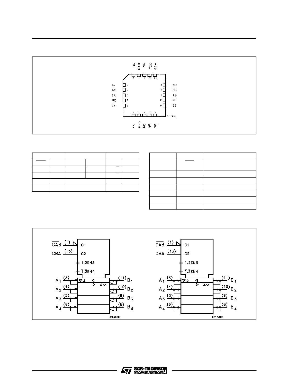
CHIP CARRIER
TRUTH TABLE
INPUTS FUNCTION OUTPUTS
GAB GBA A BUS B BUS HC242 HC243
H H OUTPUT INPUT A = B A = B
L L INPUT OUTPUT B = A B = A
H L HIGH IMPEDANCE Z Z
L H HIGH IMPEDANCE Z Z
IEC LOGIC SYMBOLS
HC242 HC243
PIN DESCRIPTI ON
PIN No SYMBOL NAME AND FUNCTION
1 GAB Output Enable Input
(active LOW)
2, 12 NC Not connected
3, 4, 5, 6 1A to 4A Data Inputs/Outputs
11, 10, 9, 8 1B to 4B Data Inputs/Outputs
13 GBA Output Enable Input
7 GND Ground (0V)
14 V
CC
Positive Supply Voltage
2/11
Page 3
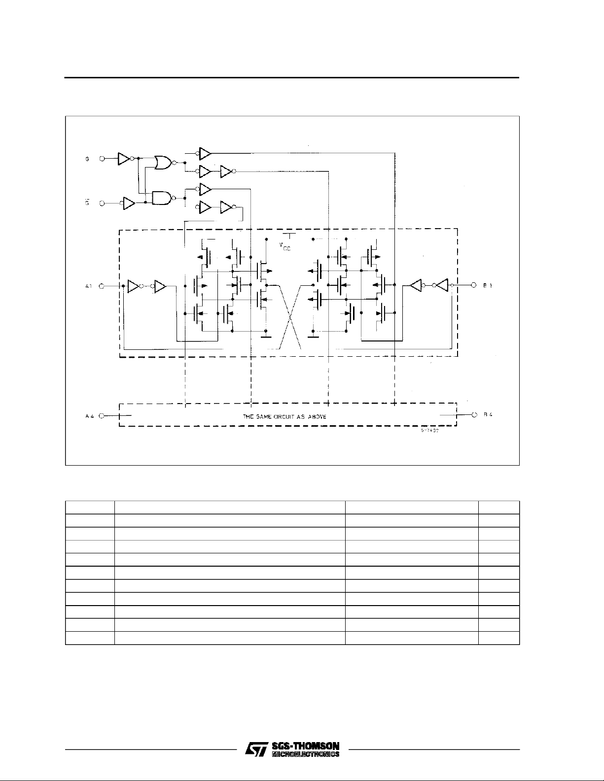
CIR CUI T D IA GR AM
M54/M74HC242/243
ABSOLU TE M AXIMU M R AT INGS
Symbol Parameter Value Unit
V
CC
V
V
O
I
IK
I
OK
I
O
I
or I
CC
P
D
T
stg
T
AbsoluteMaximumRatingsarethose values beyondwhichdamage tothedevicemayoccur. Functionaloperationunder these conditionisnotimplied.
(*)500 mW: ≅ 65oC derateto300 mWby 10mW/oC: 65oCto85oC
Supply Voltage -0.5 to +7 V
DC Input Voltage -0.5 to VCC+ 0.5 V
I
DC Output Voltage -0.5 to VCC+ 0.5 V
DC Input Diode Current ± 20 mA
DC Output Diode Current ± 20 mA
DC Output Source Sink Current Per Output Pin ± 35 mA
DC VCCor Ground Current ± 70 mA
GND
Power Dissipation 500 (*) mW
Storage Temperature -65 to +150
Lead Temperature (10sec) 300
L
o
C
o
C
3/11
Page 4
M54/M74HC242/243
RECO MM ENDED OPERAT IN G CO NDITI ONS
Symbol Parameter Value Unit
V
V
V
T
t
r,tf
DC SPECIFICATIONS
Symbol Parameter
V
IH
V
V
OH
V
OL
I
I
OZ
I
CC
Supply Voltage 2 to 6 V
CC
Input Voltage 0 to V
I
Output Voltage 0 to V
O
Operating Temperature: M54HC Series
op
M74HC Series
CC
CC
-55 to +125
-40 to +85
Input Rise and Fall Time VCC= 2 V 0 to 1000 ns
V
= 4.5 V 0 to 500
CC
V
= 6 V 0 to 400
CC
Test Conditions Value
V
(V)
CC
=25oC
T
A
54HC and 74HC
-40 to 85oC
74HC
-55 to 125oC
Min. Typ. Max. Min. Max. Min. Max.
High Level Input
Voltage
2.0 1.5 1.5 1.5
4.5 3.15 3.15 3.15
6.0 4.2 4.2 4.2
Low Level Input
IL
Voltage
2.0 0.5 0.5 0.5
4.5 1.35 1.35 1.35
6.0 1.8 1.8 1.8
High Level
Output Voltage
Low Level Output
Voltage
Input Leakage
I
Current
3 State Output
Off-state Current
Quiescent Supply
2.0
V
=
I
4.5 4.4 4.5 4.4 4.4
6.0 5.9 6.0 5.9 5.9
4.5 I
6.0 I
2.0
4.5 0.0 0.1 0.1 0.1
6.0 0.0 0.1 0.1 0.1
4.5 I
6.0 I
6.0
6.0
IO=-20 µA
V
IH
or
V
IL
=-6.0 mA 4.18 4.31 4.13 4.10
O
=-7.8 mA 5.68 5.8 5.63 5.60
O
V
=
I
IO=20µA
V
IH
or
V
IL
= 6.0 mA 0.17 0.26 0.33 0.40
O
= 7.8 mA 0.18 0.26 0.33 0.40
O
VI=VCCor GND ±0.1 ±1 ±1 µA
VI=VIHor V
VO=VCCor GND
1.9 2.0 1.9 1.9
0.0 0.1 0.1 0.1
IL
±0.5 ±5 ±10 µA
6.0 VI=VCCor GND 4 40 80 µA
Current
54HC
V
V
o
C
o
C
Unit
V
V
V
V
4/11
Page 5

M54/M74HC242/243
AC ELECTRICAL CHARACTERISTICS (Inp ut tr=tf=6ns)
Test Conditions Value
T
=25oC
Symbol Parameter
t
t
TLH
THL
Output Transition
Time
V
C
CC
(V)
L
(pF)
2.0
50
4.5 7121518
A
54HC and 74HC
Min. Typ. Max. Min. Max. Min. Max.
25 60 75 90
6.0 6101315
t
PLH
t
PHL
Propagation
Delay Time
2.0
50
4.5 13 18 23 27
39 90 115 135
6.0 11 15 20 23
2.0
150
4.5 17 29 36 44
51 145 180 220
6.0 14 25 31 37
t
t
PZH
PZL
3 State Output
Enable Time
2.0
50 RL=1KΩ
4.5 18 29 36 44
57 145 180 220
6.0 15 25 31 37
2.0
150 R
4.5 22 35 44 53
=1KΩ
L
70 175 220 265
6.0 19 30 37 45
t
t
PHZ
PLZ
3 State Output
Disable Time
2.0
50 R
4.5 20 30 38 45
=1KΩ
L
45 150 190 225
6.0 17 26 32 38
C
C
PD
(*) CPDisdefined as the value ofthe IC’sinternal equivalent capacitance which is calculated from the operating current consumption without load.
(Referto Test Circuit). Average operting current canbe obtainedbythe followingequation. ICC(opr) = CPD•VCC•fIN+I
Input Capacitance 5 10 10 10 pF
IN
(*) Power Dissipation
Capacitance
for HC242
for HC243
30
35
-40 to 85oC
74HC
-55 to 125oC
54HC
CC
Unit
ns
ns
ns
ns
ns
ns
pF
SWITCHING CHARACTERISTICS TEST WAVEFORM
5/11
Page 6

M54/M74HC242/243
TEST CIRCUIT ICC(Opr.) CCPCALCULATION
CPDisto be calculated withthe following formula
by usingthemeasuredvalueof ICC(Opr.)in the
test circuitopposite
I
(
Opr
CPD=
CC
fINxV
In determining the typical value of CPD, a
relatively high frequencyof 1MHzwasapplied to
fIN, inorderto eliminateany error causedbythe
quiescent supplycurrent.
.)
CC
6/11
Page 7

Plastic DIP14 MECHANICAL DATA
M54/M74HC242/243
DIM.
MIN. TYP. MAX. MIN. TYP. MAX.
a1 0.51 0.020
B 1.39 1.65 0.055 0.065
b 0.5 0.020
b1 0.25 0.010
D 20 0.787
E 8.5 0.335
e 2.54 0.100
e3 15.24 0.600
F 7.1 0.280
I 5.1 0.201
L 3.3 0.130
Z 1.27 2.54 0.050 0.100
mm inch
P001A
7/11
Page 8

M54/M74HC242/243
Ceramic DIP14/1 MECHANICAL DATA
DIM.
MIN. TYP. MAX. MIN. TYP. MAX.
A 20 0.787
B 7.0 0.276
D 3.3 0.130
E 0.38 0.015
e3 15.24 0.600
F 2.29 2.79 0.090 0.110
G 0.4 0.55 0.016 0.022
H 1.17 1.52 0.046 0.060
L 0.22 0.31 0.009 0.012
M 1.52 2.54 0.060 0.100
N 10.3 0.406
P 7.8 8.05 0.307 0.317
Q 5.08 0.200
mm inch
8/11
P053C
Page 9

SO14 MECHANICAL DATA
M54/M74HC242/243
DIM.
MIN. TYP. MAX. MIN. TYP. MAX.
A 1.75 0.068
a1 0.1 0.2 0.003 0.007
a2 1.65 0.064
b 0.35 0.46 0.013 0.018
b1 0.19 0.25 0.007 0.010
C 0.5 0.019
c1 45° (typ.)
D 8.55 8.75 0.336 0.344
E 5.8 6.2 0.228 0.244
e 1.27 0.050
e3 7.62 0.300
F 3.8 4.0 0.149 0.157
G 4.6 5.3 0.181 0.208
L 0.5 1.27 0.019 0.050
M 0.68 0.026
S8°(max.)
mm inch
P013G
9/11
Page 10

M54/M74HC242/243
PLCC20 MECHANICAL DATA
DIM.
MIN. TYP. MAX. MIN. TYP. MAX.
A 9.78 10.03 0.385 0.395
B 8.89 9.04 0.350 0.356
D 4.2 4.57 0.165 0.180
d1 2.54 0.100
d2 0.56 0.022
E 7.37 8.38 0.290 0.330
e 1.27 0.050
e3 5.08 0.200
F 0.38 0.015
G 0.101 0.004
M 1.27 0.050
M1 1.14 0.045
mm inch
10/11
P027A
Page 11

M54/M74HC242/243
Information furnishedis believed to be accurate and reliable. However, SGS-THOMSON Microelectronicsassumes no responsability for the
consequences of useof suchinformation nor for any infringementof patents or other rightsof third parties which may results from its use. No
license is granted byimplication or otherwiseunder any patentor patentrights ofSGS-THOMSON Microelectronics. Specificationsmentioned
in thispublication are subjectto changewithout notice. This publicationsupersedes andreplaces all information previouslysupplied.
SGS-THOMSON Microelectronicsproducts are not authorized foruse ascritical componentsinlife supportdevices or systems without express
written approval of SGS-THOMSON Microelectonics.
1994SGS-THOMSON Microelectronics- All Rights Reserved
Australia -Brazil - France - Germany - Hong Kong - Italy -Japan - Korea -Malaysia - Malta - Morocco - The Netherlands -
Singapore -Spain - Sweden- Switzerland - Taiwan - Thailand - UnitedKingdom - U.S.A
SGS-THOMSON Microelectronics GROUP OFCOMPANIES
11/11
 Loading...