

Page 1
.HIGH SPEED
tPD= 12 ns(TYP.) at VCC=5V
.LOWPOWERDISSIPATION
ICC=4µA(MAX.) AT TA=25°C
.HIGH NOISEIMMUNITY
V
NIH=VNIL
=28%VCC(MIN.)
.OUTPUT DRIVE CAPABILITY
10 LSTTL LOADS
.SYMMETRICALOUTPUT IMPEDANCE
IOH =IOL= 4 mA(MIN.)
.BALANCEDPROPAGATION DELAYS
t
PLH=tPHL
.WIDE OPERATINGVOLTAGE RANGE
VCC(OPR)= 2 V TO6 V
.PIN ANDFUNCTION COMPATIBLE
WITH 54/74LS237
M54HC237
M74HC237
3 TO8 LINE DECODER LATCH
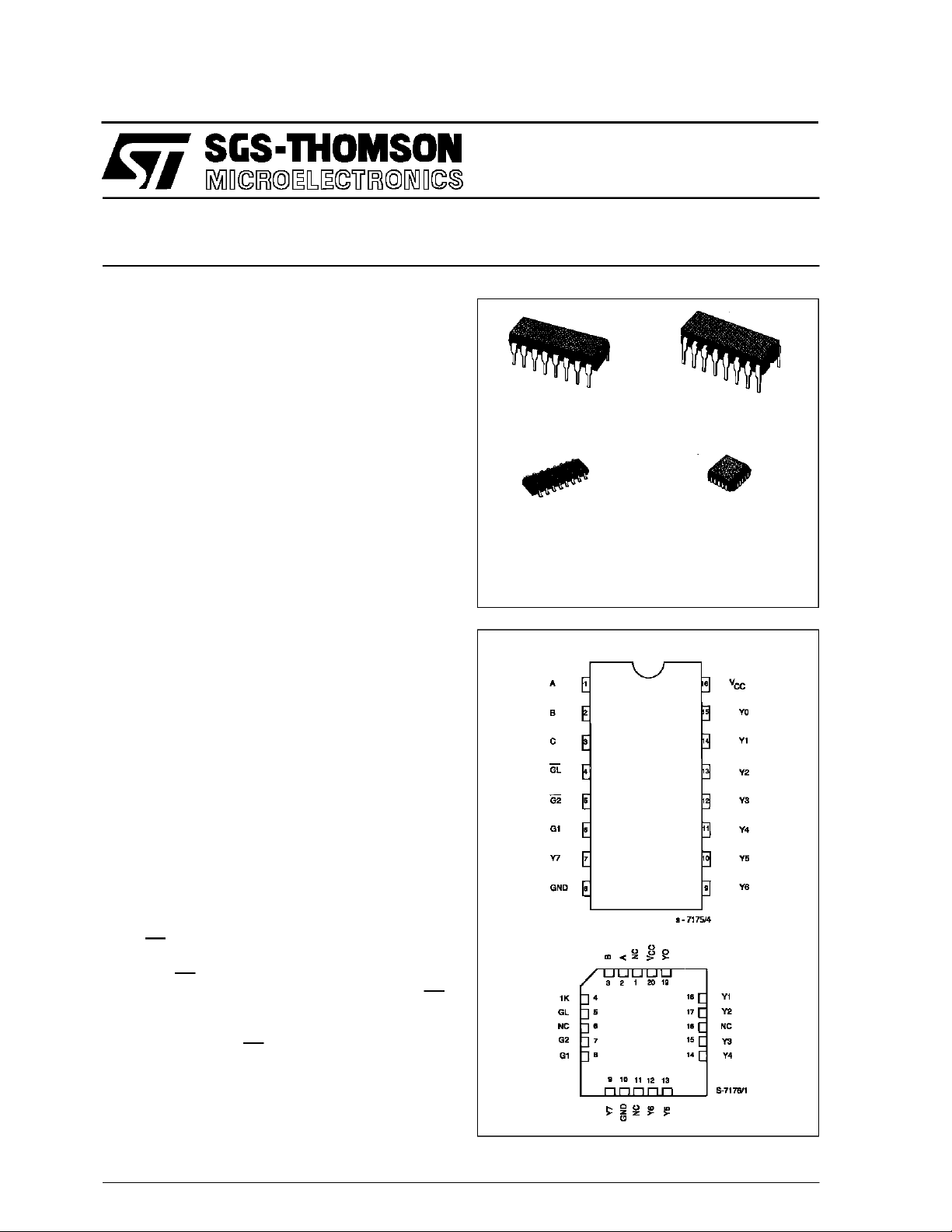
B1R
(PlasticPackage)
M1R
(MicroPackage)
ORDER CODES :
M54HC 237F1R M74H C237M1R
M74HC 237B1R M74HC2 37C1R
F1R
(CeramicPackage)
C1R
(Chip Carrier)
DESCRIPTION
The M54/74HC237 is a high speed CMOS 3 TO 8
LINE DECODER LATCH fabricated in silicon gate
C2MOStechnology.
It has the same high speed performance of LSTTL
combined with true CMOS low power consumption.
WhenGL goes from low to high, the address present
atthe select inputs (A, B, C) isstored in thelatches.
Aslong as GLremains highno address changes will
be recognized. Output enable controls, G1 and G2
control the state of the outputs independantly of the
selector latch-enableinputs. Alloftheoutputs are low
unless G1is high andG2is low. The ’HC237 is ideally
suited for the implementation of glitch-free decoders
in stored-address applications in bus oriented systems. Allinputs areequipped with protection circuits
againststatic discharge andtransient excessvoltage.
NC =
No Internal
Connection
PIN CONNECTIONS(top view)
October 1992
1/11
Page 2
M54/M74HC237
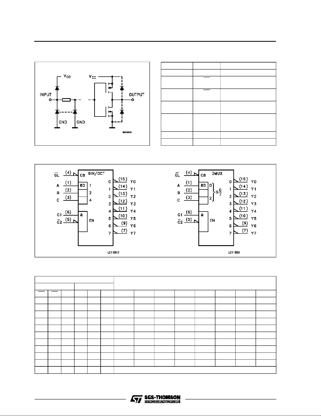
INPUT AND OUTPUT EQUIVALENT CIRCUIT
IEC LOGIC SYMBOLS
PIN DESCRIPTION
PIN No SYMBOL NAME AND FUNCTION
1, 2, 3 A, B, C Data Inputs
4 GL Latch Enable Input
(Active LOW)
5 G2 Data Enable Input
(Active LOW)
6 G1 Data Enable Input
(Active HIGH)
15, 14, 13,
12, 11, 10, 9,
7
8 GND Ground (0V)
16 V
Y0 to Y7 Decoder Outputs
CC
Positive Supply Voltage
TRUTH TABLE
INPUTS
ENABLE SELECT
GLG2G1CBAY0Y1Y2Y3Y4Y5Y6Y7
XXLXXXLLLLLLLL
XHXXXXLLLLLLLL
LLHLLLHLLLLLLL
LLHLLHLHLLLLLL
LLHLHLLLHLLLLL
LLHLHHLLLHLLLL
LLHHLLLLLLHLLL
LLHHLHLLLLLHLL
LLHHHLLLLLLLHL
LLHHHHLLLLLLLH
H L H X X X OUTPUT CORRESPONDING TO STORED ADDRESS, H: ALL OTHERS, L
X: Don’t Care
2/11
OUTPUS
Page 3
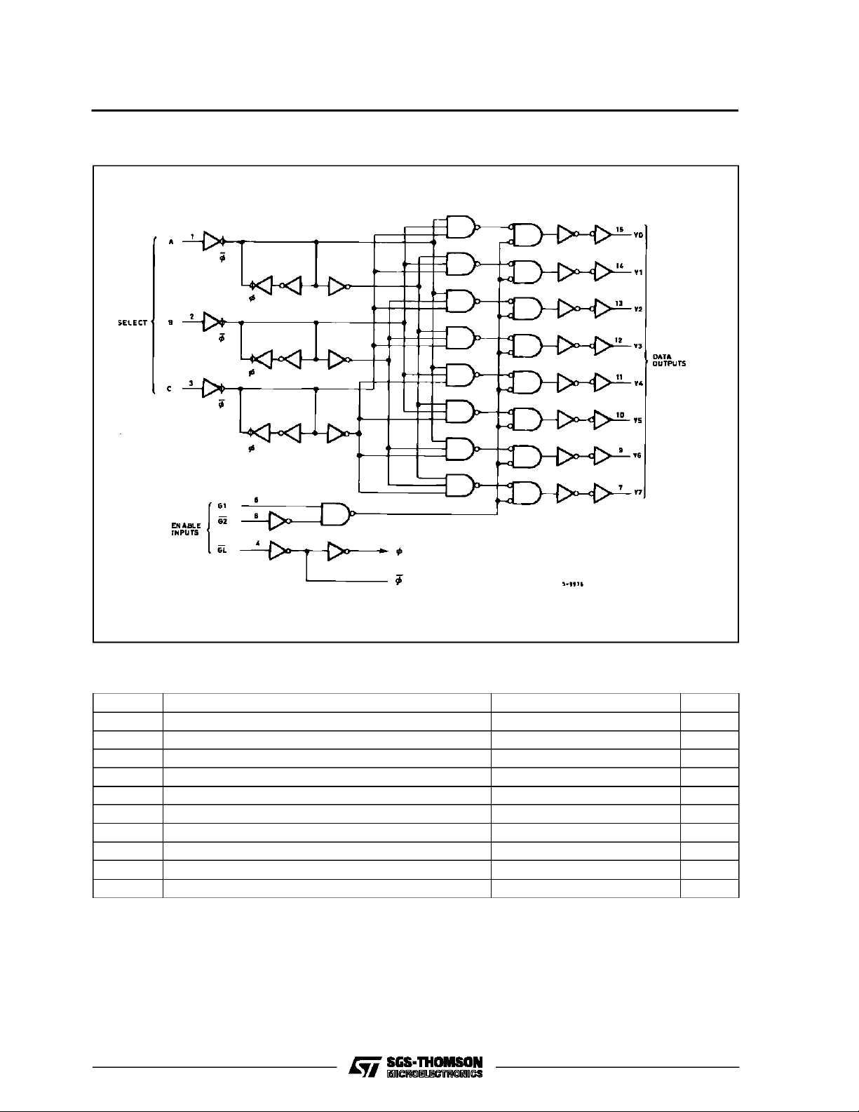
LOGIC DIAGRAM
M54/M74HC237
ABSOLU TE M AXI MU M R AT INGS
Symbol Parameter Value Unit
V
CC
V
V
O
I
IK
I
OK
I
O
I
or I
CC
P
D
T
stg
T
AbsoluteMaximumRatingsarethose valuesbeyond whichdamage to thedevice mayoccur.Functional operation under these conditionisnotimplied.
(*)500 mW: ≅ 65oC derateto300 mWby 10mW/oC: 65oCto85oC
Supply Voltage -0.5 to +7 V
DC Input Voltage -0.5 to VCC+ 0.5 V
I
DC Output Voltage -0.5 to VCC+ 0.5 V
DC Input Diode Current ± 20 mA
DC Output Diode Current ± 20 mA
DC Output Source Sink Current Per Output Pin ± 25 mA
DC VCCor Ground Current ± 50 mA
GND
Power Dissipation 500 (*) mW
Storage Temperature -65 to +150
Lead Temperature (10 sec) 300
L
o
C
o
C
3/11
Page 4
M54/M74HC237
RECO MM ENDED O PERAT IN G CONDI TIONS
Symbol Parameter Value Unit
V
V
V
T
t
r,tf
DC SPECIFICATIO NS
Symbol Parameter
V
IH
V
V
OH
V
OL
I
I
CC
Supply Voltage 2 to 6 V
CC
Input Voltage 0 to V
I
Output Voltage 0 to V
O
Operating Temperature: M54HC Series
op
M74HC Series
CC
CC
-55 to +125
-40 to +85
Input Rise and Fall Time VCC= 2 V 0 to 1000 ns
V
= 4.5 V 0 to 500
CC
V
= 6 V 0 to 400
CC
Test Conditions Value
T
High Level Input
Voltage
=25oC
V
(V)
CC
A
54HC and 74HC
Min. Typ. Max. Min. Max. Min. Max.
2.0 1.5 1.5 1.5
4.5 3.15 3.15 3.15
-40 to 85oC
74HC
-55 to 125oC
6.0 4.2 4.2 4.2
Low Level Input
IL
Voltage
2.0 0.5 0.5 0.5
4.5 1.35 1.35 1.35
6.0 1.8 1.8 1.8
High Level
Output Voltage
Low Level Output
Voltage
Input Leakage
I
Current
Quiescent Supply
2.0
V
=
I
4.5 4.4 4.5 4.4 4.4
6.0 5.9 6.0 5.9 5.9
4.5 I
6.0 I
2.0
4.5 0.0 0.1 0.1 0.1
6.0 0.0 0.1 0.1 0.1
4.5 I
6.0 I
6.0
IO=-20 µA
V
IH
or
V
IL
=-4.0 mA 4.18 4.31 4.13 4.10
O
=-5.2 mA 5.68 5.8 5.63 5.60
O
=
V
I
IO=20µA
V
IH
or
V
IL
= 4.0 mA 0.17 0.26 0.33 0.40
O
= 5.2 mA 0.18 0.26 0.33 0.40
O
VI=VCCor GND ±0.1 ±1 ±1 µA
1.9 2.0 1.9 1.9
0.0 0.1 0.1 0.1
6.0 VI=VCCor GND 4 40 80 µA
Current
54HC
V
V
o
C
o
C
Unit
V
V
V
V
4/11
Page 5

M54/M74HC237
AC ELECTRICAL CHARACTERI STI CS (CL=50pF,Inputtr=tf=6ns)
Test Conditions Value
=25oC
T
Symbol Parameter
t
t
TLH
THL
Output Transition
Time
V
CC
(V)
2.0 30 75 95 115
4.5 8151922
A
54HC and 74HC
Min. Typ. Max. Min. Max. Min. Max.
6.0 7131619
t
PLH
t
PHL
t
PLH
t
PHL
t
PLH
t
PHL
t
PLH
t
PHL
t
W(L)
C
C
PD
Propagation
Delay Time
(A, B, C - Y)
Propagation
Delay Time
(G1 - Y)
Propagation
Delay Time
(G2 - Y)
Propagation
Delay Time
(GL - Y)
Minimum Pulse
Width
(GL)
t
Minimum Set-up
s
Time
(A, B, C - GL)
t
Minimum Hold
h
Time
(A, B, C - GL)
Input Capacitance 5 10 10 10 pF
IN
(*) Power Dissipation
2.0 60 180 225 270
4.5 19 36 45 54
6.0 16 31 38 46
2.0 45 140 175 210
4.5 15 28 35 42
6.0 13 24 30 36
2.0 45 140 175 210
4.5 15 28 35 42
6.0 13 24 30 36
2.0 65 190 240 285
4.5 21 38 48 57
6.0 18 32 41 48
2.0 10 75 95 110
4.5 6151922
6.0 6131619
2.0 12 50 65 75
4.5 3101315
6.0 2 9 11 13
2.0 25 30 40
4.5 5 6 8
6.0 5 5 7
52
Capacitance
(*) CPDisdefined as the value ofthe IC’sinternal equivalent capacitance which is calculated fromthe operatingcurrent consumption without load.
-40 to 85oC
74HC
-55 to 125oC
54HC
Unit
ns
ns
ns
ns
ns
ns
ns
ns
pF
SWITCHING CHARACTERISTICS TEST WAVEFORM
5/11
Page 6
M54/M74HC237
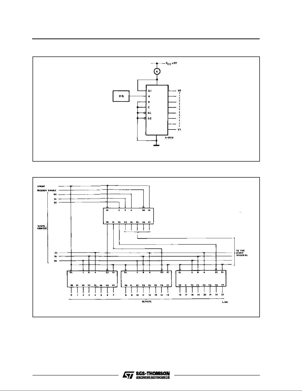
TEST CIRCUIT ICC(Opr.)
INPUTTRANSITIONTIMEISTHESAMEASTHATINCASE OFSWITCHING CHARACTERISTICSTEST.
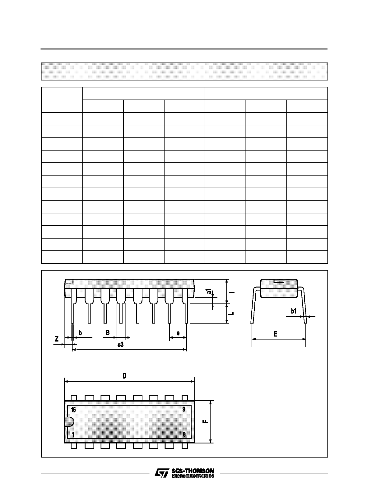
6 Line to 64 LineDecoder with Input Address Storage.
6/11
Page 7
Plastic DIP16 (0.25) MECHANICAL DATA
M54/M74HC237
DIM.
MIN. TYP. MAX. MIN. TYP. MAX.
a1 0.51 0.020
B 0.77 1.65 0.030 0.065
b 0.5 0.020
b1 0.25 0.010
D 20 0.787
E 8.5 0.335
e 2.54 0.100
e3 17.78 0.700
F 7.1 0.280
I 5.1 0.201
L 3.3 0.130
Z 1.27 0.050
mm inch
P001C
7/11
Page 8

M54/M74HC237
Ceramic DIP16/1 MECHANICAL DATA
DIM.
MIN. TYP. MAX. MIN. TYP. MAX.
A 20 0.787
B 7 0.276
D 3.3 0.130
E 0.38 0.015
e3 17.78 0.700
F 2.29 2.79 0.090 0.110
G 0.4 0.55 0.016 0.022
H 1.17 1.52 0.046 0.060
L 0.22 0.31 0.009 0.012
M 0.51 1.27 0.020 0.050
N 10.3 0.406
P 7.8 8.05 0.307 0.317
Q 5.08 0.200
mm inch
8/11
P053D
Page 9
SO16 (Narrow) MECHANICAL DATA
M54/M74HC237
DIM.
MIN. TYP. MAX. MIN. TYP. MAX.
A 1.75 0.068
a1 0.1 0.2 0.004 0.007
a2 1.65 0.064
b 0.35 0.46 0.013 0.018
b1 0.19 0.25 0.007 0.010
C 0.5 0.019
c1 45° (typ.)
D 9.8 10 0.385 0.393
E 5.8 6.2 0.228 0.244
e 1.27 0.050
e3 8.89 0.350
F 3.8 4.0 0.149 0.157
G 4.6 5.3 0.181 0.208
L 0.5 1.27 0.019 0.050
M 0.62 0.024
S8°(max.)
mm inch
P013H
9/11
Page 10

M54/M74HC237
PLCC20 MECHANICAL DATA
DIM.
MIN. TYP. MAX. MIN. TYP. MAX.
A 9.78 10.03 0.385 0.395
B 8.89 9.04 0.350 0.356
D 4.2 4.57 0.165 0.180
d1 2.54 0.100
d2 0.56 0.022
E 7.37 8.38 0.290 0.330
e 1.27 0.050
e3 5.08 0.200
F 0.38 0.015
G 0.101 0.004
M 1.27 0.050
M1 1.14 0.045
mm inch
10/11
P027A
Page 11

M54/M74HC237
Information furnishedis believed to be accurate and reliable. However, SGS-THOMSON Microelectronicsassumes no responsability for the
consequences of useof suchinformation nor for any infringement of patents or other rights of third parties which may results from its use. No
license is granted byimplication or otherwiseunder any patentor patentrights ofSGS-THOMSON Microelectronics. Specificationsmentioned
in this publication are subjectto changewithout notice. This publication supersedes andreplaces all information previouslysupplied.
SGS-THOMSON Microelectronicsproducts are not authorized foruse ascritical componentsin life supportdevices or systems without express
written approval of SGS-THOMSON Microelectonics.
1994SGS-THOMSON Microelectronics- All Rights Reserved
Australia -Brazil - France - Germany - Hong Kong - Italy - Japan - Korea - Malaysia - Malta -Morocco - The Netherlands-
Singapore -Spain - Sweden- Switzerland - Taiwan - Thailand - UnitedKingdom - U.S.A
SGS-THOMSON Microelectronics GROUP OFCOMPANIES
11/11
 Loading...