

Page 1
.HIGH SPEED
tPD= 13 ns(TYP.) at VCC=5V
.LOWPOWERDISSIPATION
ICC=4µA(MAX.) at TA=25°C6V
.HIGH NOISEIMMUNITY
V
NIH=VNIL
=28%VCC(MIN.)
.OUTPUT DRIVE CAPABILITY
10 LSTTL LOADS
.SYMMETRICALOUTPUT IMPEDANCE
IOH =IOL= 4 mA(MIN.)
.BALANCEDPROPAGATION DELAYS
t
PLH=tPHL
.WIDE OPERATINGVOLTAGE RANGE
VCC(OPR)= 2 V to 6 V
.PIN ANDFUNCTION COMPATIBLE
WITH 54/74LS195
M54HC195
M74HC195
8 BITPIPO SHIFT REGISTER
B1R
(PlasticPackage)
M1R
(MicroPackage)
ORDER CODES :
M54HC 195F1R M74H C195M1R
M74HC 195B1R M74HC1 95C1R
F1R
(CeramicPackage)
C1R
(Chip Carrier)
DESCRIPTION
The M54/74HC195 is a high speed CMOS 4 BIT
PIPO SHIFT REGISTER fabricated in silicon gate
C2MOStechnology. Ithasthesamehighspeedperformance of LSTTL combined with true CMOS low
powerconsumption.
This shift register features parallel inputs, parallel
outputs, J-K serial inputs, a SHIFT/LOAD control
input,and a directoverridingCLEAR. Thisshift registercan operate intwo modes : Parallel Load ;Shift
from QAtowards QD.
Parallel loadingisaccomplishedbyapplying the four
bits of data, and taking the SHIFT/LOAD control
inputlow. The datais loaded intotheassociated flip
flops and appears at the outputs after the positive
transitionof the clockinput.During parallel loading,
serial data flow is inhibited. Serial shifting occurs
synchronously whenthe SHIFT/LOAD controlinput
ishigh.Serial data forthis mode isenteredattheJ-K
inputs. These inputs allowthe first stageto perform
as a J-Kor TOGGLE flip flopas shown inthe truthtable.
All inputs are equipped with protection circuits
against static discharge transient excess voltage.
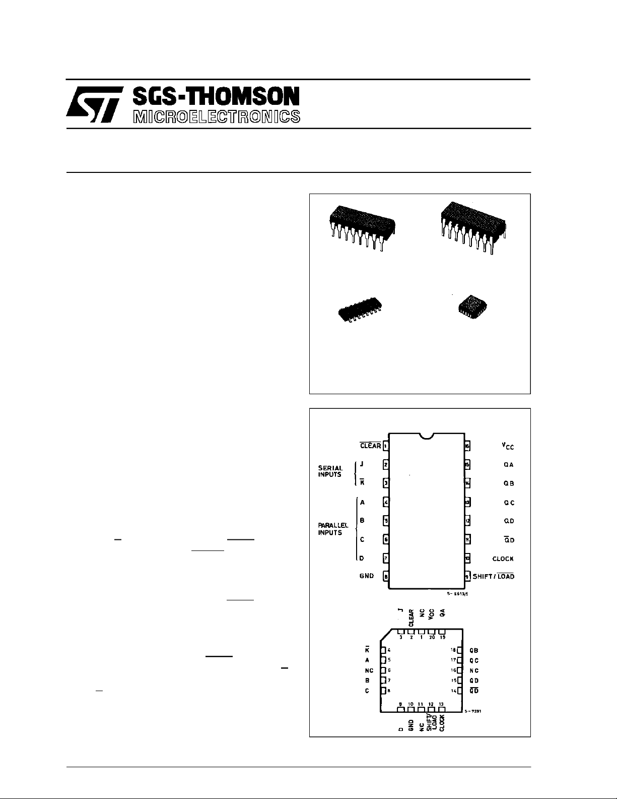
PIN CONNECTIONS(top view)
NC =
No Internal
Connection
October 1992
1/13
Page 2
M54/M74HC195
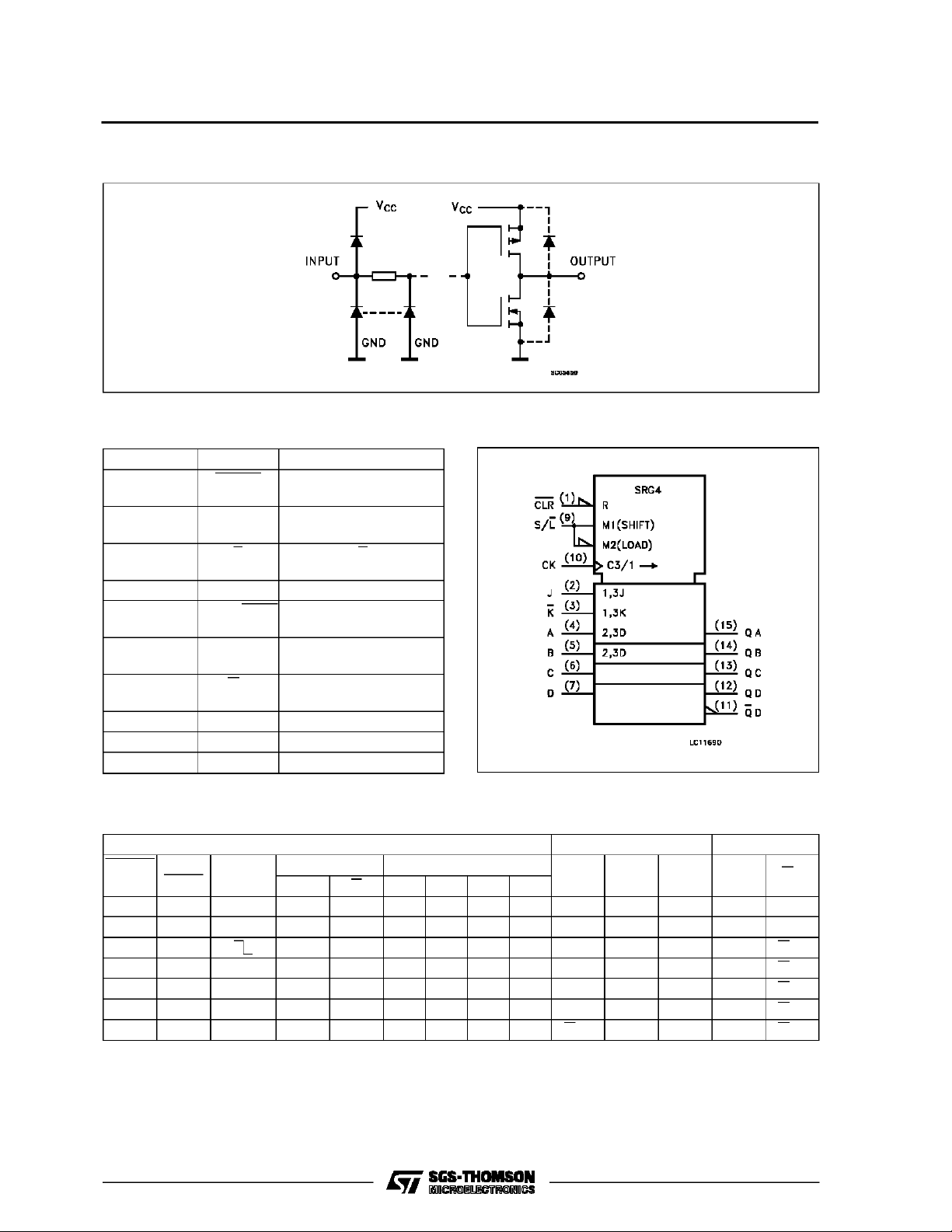
INPUT AND OUTPUT EQUIVALENT CIRCUIT
PIN DESCRIPTION
PIN No SYMBOL NAME AND FUNCTION
1 CLEAR Reset Input (Active
LOW)
2 J First Stage J Input
(Active LOW)
3 K First Stage K Input
(Active LOW)
4, 5, 6, 7 A to D Parallel Data Input
9 SHIFT/LOAD Control Input
10 CLOCK Clock Input (LOW to
HIGH Edge-triggered)
11 QD Inverted Output From
The Last Stage
15, 14, 13, 12 QA to QD Paralle Outputs
8 GND Ground (0V)
16 V
CC
Positive Supply Voltage
IEC LOGIC SYMBOL
TRUTH TABLE
INPUTS OUTPUS
CLEAR SHIFT/
LOAD
L X X X X XXXX L L L L L
HL XXabcdabcdd
H H X X XXXXQA0QB0QC0QD0QD0
H H L H XXXXQA0QA0QBnQCnQCn
H H L L XXXX L QAnQBnQCnQCn
H H H H XXXX HQAnQBnQCnQCn
H H H L XXXXQAnQAnQBnQCnQCn
X: Don’t Care: The level of QA,QB, QC, respectively, before the mst recent positivetransition of theclock.
CLOCK
SERIAL PARALLEL
J K ABCD
QA QB QC QD QD
2/13
Page 3
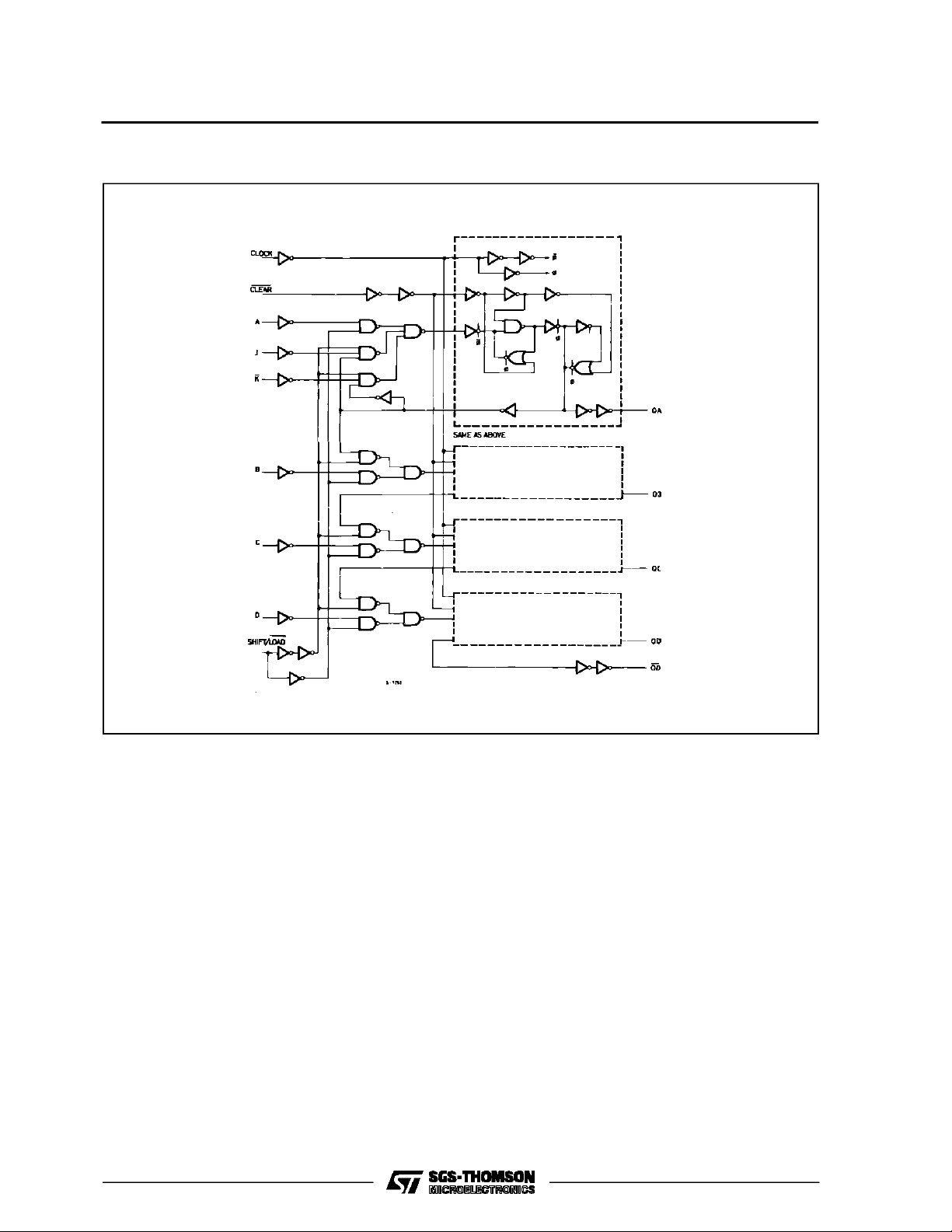
LOGIC DIAGRAM
M54/M74HC195
3/13
Page 4
M54/M74HC195
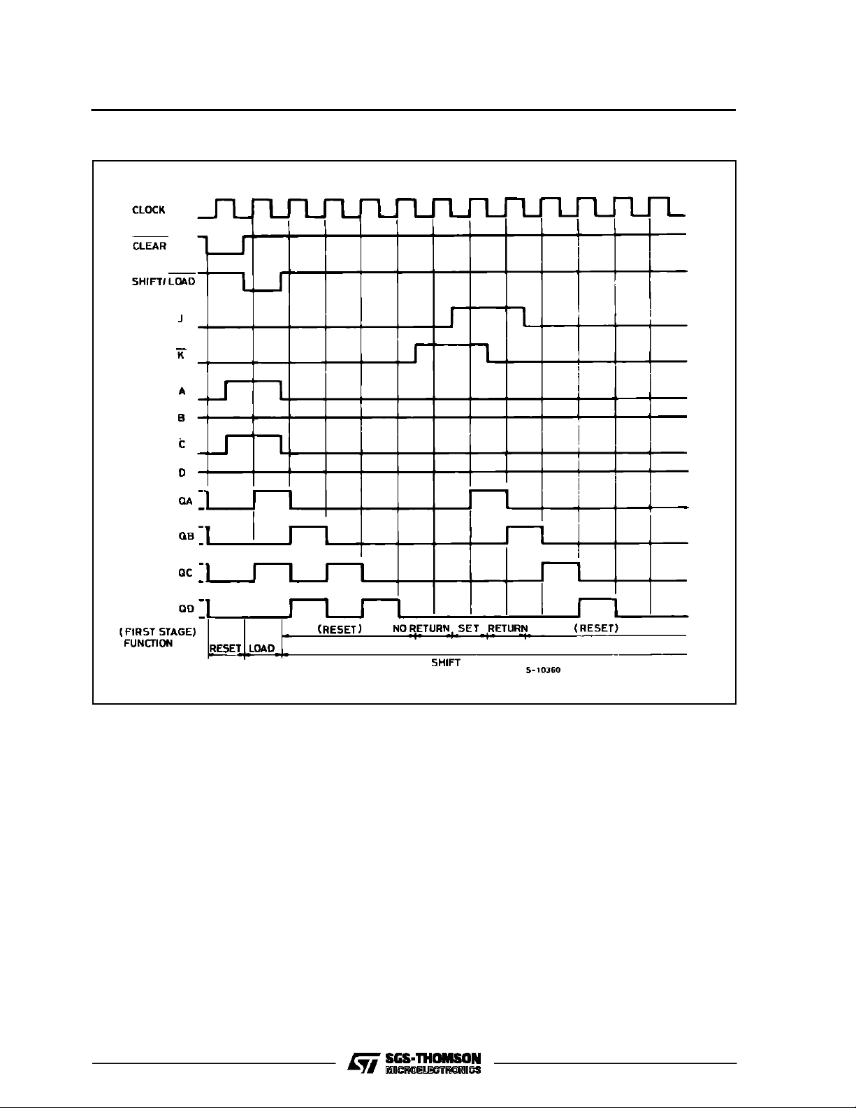
TIMING CHART
4/13
Page 5

M54/M74HC195
ABSOLU TE MAXIMU M RATINGS
Symbol Parameter Value Unit
V
CC
V
V
O
I
IK
I
OK
I
O
I
or I
CC
P
D
T
stg
T
L
AbsoluteMaximumRatingsarethose valuesbeyond whichdamage to thedevice mayoccur.Functional operation under these conditionisnotimplied.
(*)500 mW: ≅ 65oC derateto300 mWby 10mW/oC: 65oCto85oC
RECO MM ENDED O PERAT IN G C O NDITI ONS
Symbol Parameter Value Unit
V
CC
V
I
V
O
T
op
t
r,tf
Supply Voltage -0.5 to +7 V
DC Input Voltage -0.5 to VCC+ 0.5 V
I
DC Output Voltage -0.5 to VCC+ 0.5 V
DC Input Diode Current ± 20 mA
DC Output Diode Current ± 20 mA
DC Output Source Sink Current Per Output Pin ± 25 mA
DC VCCor Ground Current ± 50 mA
GND
Power Dissipation 500 (*) mW
Storage Temperature -65 to +150
Lead Temperature (10 sec) 300
Supply Voltage 2 to 6 V
Input Voltage 0 to V
Output Voltage 0 to V
Operating Temperature: M54HC Series
M74HC Series
CC
CC
-55 to +125
-40 to +85
Input Rise and Fall Time VCC= 2 V 0 to 1000 ns
V
= 4.5 V 0 to 500
CC
V
= 6 V 0 to 400
CC
o
C
o
C
V
V
o
C
o
C
5/13
Page 6

M54/M74HC195
DC SPECIFICATIO NS
Symbol Parameter
V
V
V
V
I
High Level Input
IH
Voltage
Low Level Input
IL
Voltage
High Level
OH
Output Voltage
Low Level Output
OL
Voltage
I
Input Leakage
I
Current
Quiescent Supply
CC
Current
Test Conditions Value
V
(V)
CC
=25oC
A
54HC and 74HC
Min. Typ. Max. Min. Max. Min. Max.
-40 to 85oC
74HC
-55 to 125oC
54HC
Unit
T
2.0 1.5 1.5 1.5
4.5 3.15 3.15 3.15
6.0 4.2 4.2 4.2
2.0 0.5 0.5 0.5
4.5 1.35 1.35 1.35
6.0 1.8 1.8 1.8
2.0
4.5 4.4 4.5 4.4 4.4
6.0 5.9 6.0 5.9 5.9
4.5 I
6.0 I
2.0
4.5 0.0 0.1 0.1 0.1
6.0 0.0 0.1 0.1 0.1
4.5 I
6.0 I
6.0
=
V
I
IO=-20 µA
V
IH
or
V
IL
=-4.0 mA 4.18 4.31 4.13 4.10
O
=-5.2 mA 5.68 5.8 5.63 5.60
O
V
=
I
IO=20µA
V
IH
or
V
IL
= 4.0 mA 0.17 0.26 0.33 0.40
O
= 5.2 mA 0.18 0.26 0.33 0.40
O
VI=VCCor GND ±0.1 ±1 ±1 µA
1.9 2.0 1.9 1.9
0.0 0.1 0.1 0.1
6.0 VI=VCCor GND 4 40 80 µA
V
V
V
V
6/13
Page 7

M54/M74HC195
AC ELECTRICAL CHARACTERISTICS (CL=50pF,Inputtr=tf=6ns)
Test Conditions Value
T
=25oC
Symbol Parameter
t
t
TLH
THL
Output Transition
Time
V
CC
(V)
2.0 30 75 95 115
4.5 8151923
A
54HC and 74HC
Min. Typ. Max. Min. Max. Min. Max.
6.0 7131620
t
PLH
t
PHL
t
PLH
t
PHL
f
MAX
Propagation
Delay Time
(CLOCK- Qn, QD)
Propagation
Delay Time
(CLEAR- Qn, QD)
Maximum Clock
Frequency
2.0 48 125 155 190
4.5 16 25 31 38
6.0 14 21 26 32
2.0 45 120 150 180
4.5 15 24 30 36
6.0 13 20 26 31
2.0 7.6 15 6 5
4.5 38 60 30 25
6.0 45 71 35 30
t
W(H)
t
W(L)
Minimum Pulse
Width
(CLOCK)
t
W(L)
Minimum Pulse
Width
(CLEAR)
Minimum Set-up
t
s
Time
(PI)
Minimum Set-up
t
s
Time
(J, K, S/L)
Minimum Hold
t
h
Time
2.0 20 75 95 115
4.5 5151923
6.0 4131620
2.0 20 75 95 115
4.5 5151923
6.0 4131620
2.0 28 75 95 115
4.5 7151923
6.0 6131620
2.0 28 75 95 115
4.5 7151923
6.0 6131620
2.0 0 0 0
4.5 0 0 0
6.0 0 0 0
t
REM
Minimum
Removal Time
2.0 5 5 5
4.5 5 5 5
6.0 5 5 5
C
C
PD
Input Capacitance 5 10 10 10 pF
IN
(*) Power Dissipation
72
Capacitance
(*) CPDisdefined as the value ofthe IC’sinternal equivalent capacitance which is calculated fromthe operatingcurrent consumption without load.
(Referto Test Circuit). Average operting current canbe obtained bythe followingequation. ICC(opr) = CPD•VCC•fIN+I
-40 to 85oC
74HC
-55 to 125oC
54HC
CC
Unit
ns
ns
ns
MHz
ns
ns
ns
ns
ns
ns
pF
7/13
Page 8

M54/M74HC195
SWITCHING CHARACTERISTICS TEST WAVEFORM
TEST CIRCUIT ICC(Opr.)
TRANSITIONTIME OF INPUT WAVEFORM IS THESAME AS THATIN CASEOF SWITCHINGCHARACTERISTICS TEST.
8/13
Page 9

Plastic DIP16 (0.25) MECHANICAL DATA
M54/M74HC195
DIM.
MIN. TYP. MAX. MIN. TYP. MAX.
a1 0.51 0.020
B 0.77 1.65 0.030 0.065
b 0.5 0.020
b1 0.25 0.010
D 20 0.787
E 8.5 0.335
e 2.54 0.100
e3 17.78 0.700
F 7.1 0.280
I 5.1 0.201
L 3.3 0.130
Z 1.27 0.050
mm inch
P001C
9/13
Page 10

M54/M74HC195
Ceramic DIP16/1 MECHANICAL DATA
DIM.
MIN. TYP. MAX. MIN. TYP. MAX.
A 20 0.787
B 7 0.276
D 3.3 0.130
E 0.38 0.015
e3 17.78 0.700
F 2.29 2.79 0.090 0.110
G 0.4 0.55 0.016 0.022
H 1.17 1.52 0.046 0.060
L 0.22 0.31 0.009 0.012
M 0.51 1.27 0.020 0.050
N 10.3 0.406
P 7.8 8.05 0.307 0.317
Q 5.08 0.200
mm inch
10/13
P053D
Page 11

SO16 (Narrow) MECHANICAL DATA
M54/M74HC195
DIM.
MIN. TYP. MAX. MIN. TYP. MAX.
A 1.75 0.068
a1 0.1 0.2 0.004 0.007
a2 1.65 0.064
b 0.35 0.46 0.013 0.018
b1 0.19 0.25 0.007 0.010
C 0.5 0.019
c1 45° (typ.)
D 9.8 10 0.385 0.393
E 5.8 6.2 0.228 0.244
e 1.27 0.050
e3 8.89 0.350
F 3.8 4.0 0.149 0.157
G 4.6 5.3 0.181 0.208
L 0.5 1.27 0.019 0.050
M 0.62 0.024
S8°(max.)
mm inch
P013H
11/13
Page 12
M54/M74HC195
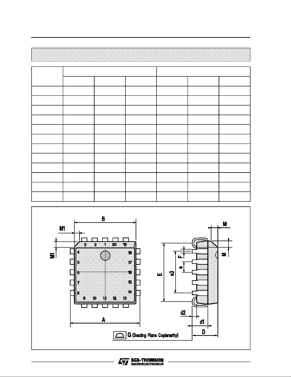
PLCC20 MECHANICAL DATA
DIM.
MIN. TYP. MAX. MIN. TYP. MAX.
A 9.78 10.03 0.385 0.395
B 8.89 9.04 0.350 0.356
D 4.2 4.57 0.165 0.180
d1 2.54 0.100
d2 0.56 0.022
E 7.37 8.38 0.290 0.330
e 1.27 0.050
e3 5.08 0.200
F 0.38 0.015
G 0.101 0.004
M 1.27 0.050
M1 1.14 0.045
mm inch
12/13
P027A
Page 13

M54/M74HC195
Information furnishedis believed to be accurate and reliable. However, SGS-THOMSON Microelectronicsassumes no responsability for the
consequences of useof suchinformation nor for any infringement of patents or other rights of third parties which may results from its use. No
license is granted byimplication or otherwiseunder any patentor patentrights ofSGS-THOMSON Microelectronics.Specificationsmentioned
in this publication are subjectto changewithout notice. This publication supersedes andreplaces all information previouslysupplied.
SGS-THOMSON Microelectronicsproducts are not authorized foruse ascritical componentsin life supportdevices or systems without express
written approval of SGS-THOMSON Microelectonics.
1994SGS-THOMSON Microelectronics- All Rights Reserved
Australia -Brazil - France - Germany - Hong Kong - Italy - Japan - Korea - Malaysia - Malta -Morocco - The Netherlands-
Singapore -Spain - Sweden- Switzerland - Taiwan - Thailand- UnitedKingdom - U.S.A
SGS-THOMSON Microelectronics GROUP OFCOMPANIES
13/13
 Loading...