

Page 1
HC192 - SYNCHRONOUS UP/DOWN DECADE COUNTER
HC193 - SYNCHRONOUS UP/DOWN BINARY COUNTER
.HIGH SPEED
f
= 54 MHz(TYP.) AT VCC=5V
MAX
.LOWPOWERDISSIPATION
ICC=4µA(MAX.) AT TA=25°C
.HIGH NOISEIMMUNITY
V
NIH=VNIL
=28%VCC(MIN.)
.OUTPUT DRIVE CAPABILITY
10 LSTTL LOADS
.SYMMETRICALOUTPUT IMPEDANCE
|IOH|=IOL=4 mA(MIN.)
.BALANCEDPROPAGATION DELAYS
t
PLH=tPHL
.WIDE OPERATINGVOLTAGERANGE
VCC(OPR)= 2 V TO6 V
.PIN AND FUNCTION COMPATIBLE WITH
54/74LS192-193
DESCRIPTION
The M54/74HC192/193 are ahigh speed CMOSSYNCHRONOUS UP/DOWNDECADE COUNTERS fabricatedinsilicon gate C2MOStechnology. They have
thesamehigh speedperformance ofLSTTLcombined
with true CMOS low power consumption. The counter
has two separate clock inputs, an UP COUNT input
and a DOWN COUNT input. All outputs of the flip-flop
are simultaneously triggered on the low to high transitionof either clock while theother inputisheldh igh. The
direction of counting is determined by which input is
clocked. This counter may be preset by entering the
desired dataon the DATAA, DATAB, DATA C, and
DATA D input.Whenthe LOADinput istaken lowthe
data is loaded independently of either clock input. This
featureallows the counters to be used asdivide-by-n
counters by modifying the count length with the preset
inputs. Inaddition thecountercanalso becleared. This
is accomplished by inputting a high on the CLEAR
input. All 4 in ternal stages are set to lowindependently
of ei ther COUNTinput. BothaB ORROWa ndCARRY
output areprovided toenablecascadingofbothupand
down counting functions. The BORROWoutput producesa negativegoingpulsewhen thecounterunderflows and the CARRY outputs a pulse when the
counter overflows. The counter can be cascaded by
connecting the CARRY and BORROW outputs of one
device to the COUNT UP and COUNTDOWN inputs,
respectively, of thenext device. Allinputs areequipped
with protection circuits against static discharge and
transient excess voltage.
M54/M74HC192
M54/M74HC193
B1R
(PlasticPackage)
M1R
(MicroPackage)
M54HC X XXF1R M74H CXXXM1R
M74HC X XXB1R M74HCX X XC1R
NC =
No Internal
Connection
ORDER CODES :
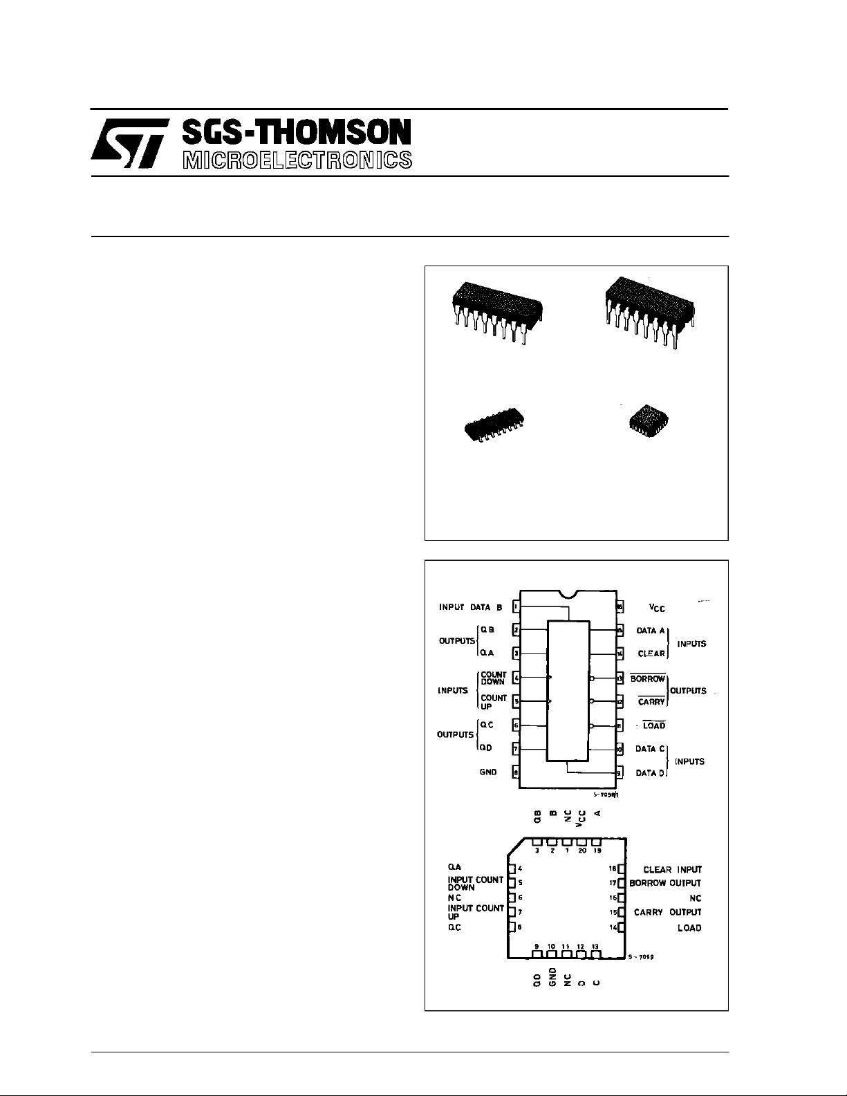
PIN CONNECTIONS(top view)
F1R
(CeramicPackage)
C1R
(Chip Carrier)
October 1992
1/15
Page 2
M54/M74HC192/193
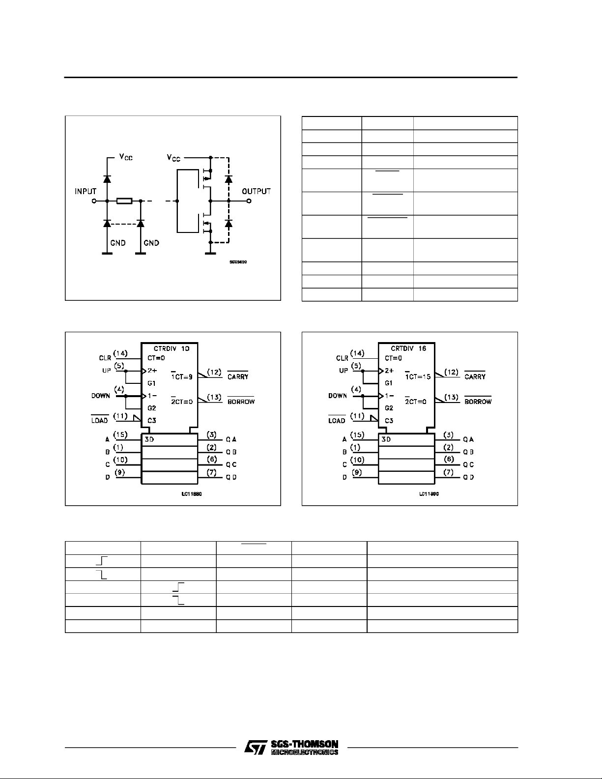
INPUT AND OUTPUT EQUIVALENT CIRCUIT
PIN DESCRIPTI ON
PIN No SYMBOL NAME AND FUNCTION
3, 2, 6, 7 QA to QD Flip-Flop Outputs
4CP
5CP
Count Down Clock Input
D
Count Up Clock Input
U
11 LOAD AsynchronousParallel
Load Input (Active LOW)
12 CARRY Count Up (Carry)
Output (Active LOW)
13 BORROW Count Down (Borrow)
Output (Active LOW)
14 CLEAR Asynchronous Reset
Input (Active HIGH)
15, 1, 10, 9 DA to DD Data Inputs
8 GND Ground (0V)
16 V
CC
Positive Supply Voltage
IEC LOGIC SYMBOL (HC193)IEC LOGIC SYMBOL (HC191)
TRUTH TABLE
COUNT UP COUNT DOWN LOAD CLEAR FUNCTION
H H L COUNT UP
H H L NO COUNT
H H L COUNT DOWN
H H L NO COUNT
X X L L PRESET
X X X H RESET
X: Don’t Care
2/15
Page 3
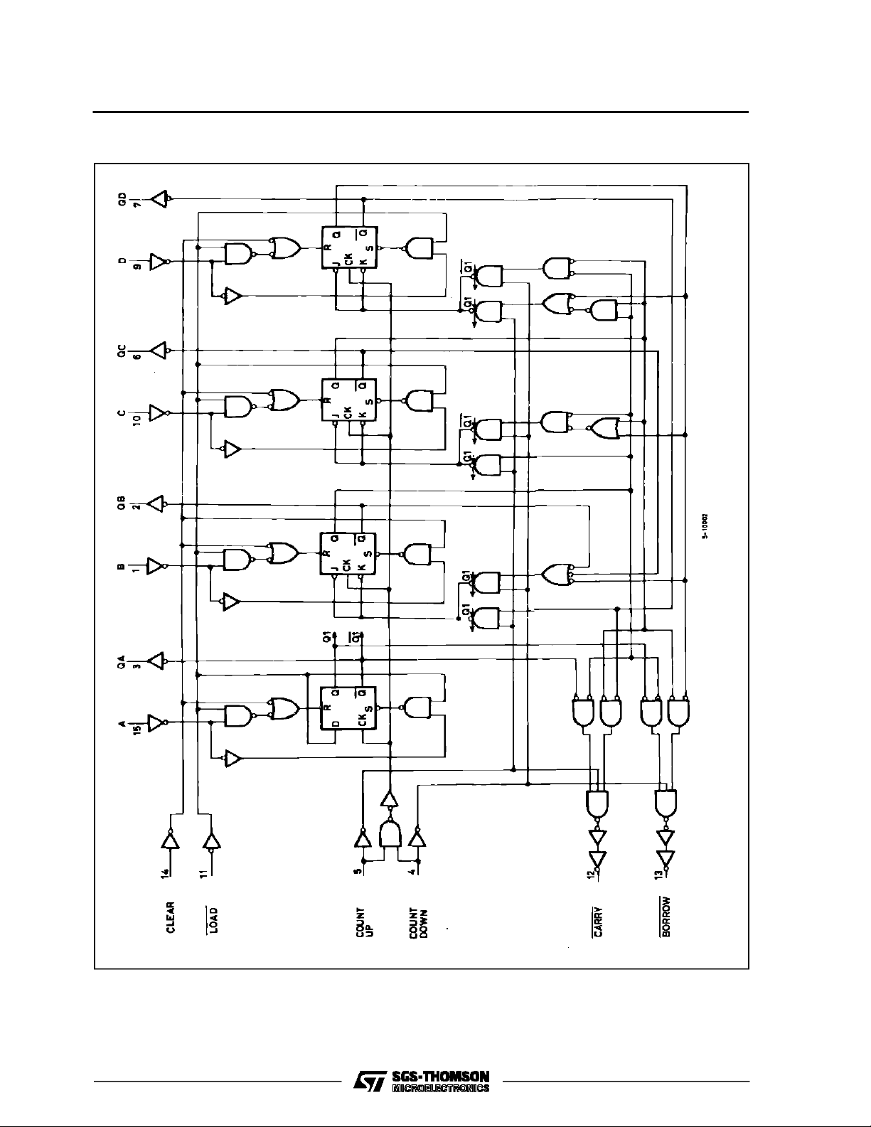
LOGIC DIAGAM (HC192)
M54/M74HC192/193
3/15
Page 4
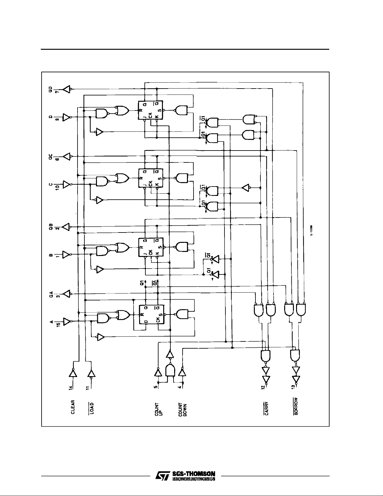
M54/M74HC192/193
LOGIC DIAGAM (HC193)
4/15
Page 5
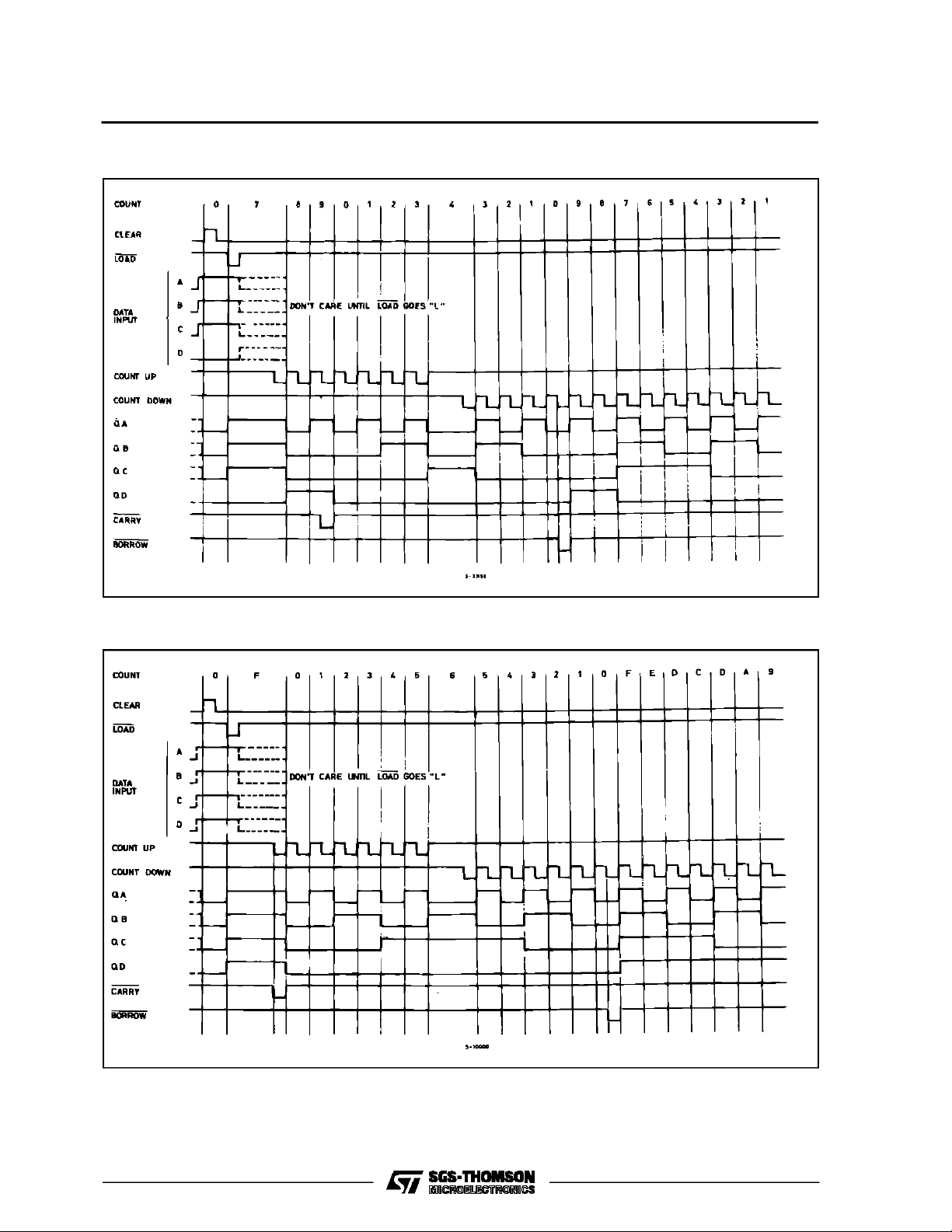
TIMING DIAGRAM (HC192)
M54/M74HC192/193
TIMING DIAGRAM (HC193)
5/15
Page 6

M54/M74HC192/193
ABSOLU TE M AXIMU M R AT INGS
Symbol Parameter Value Unit
V
CC
V
V
O
I
IK
I
OK
I
O
I
or I
CC
P
D
T
stg
T
AbsoluteMaximumRatings arethose values beyondwhichdamage tothedevicemayoccur. Functionaloperationunder theseconditionisnotimplied.
(*)500 mW: ≅ 65oC derateto 300 mWby 10mW/oC: 65oCto85oC
RECO MM ENDED OPERATIN G CO NDITI O NS
Symbol Parameter Value Unit
V
CC
V
I
V
O
T
op
t
r,tf
Supply Voltage -0.5 to +7 V
DC Input Voltage -0.5 to VCC+ 0.5 V
I
DC Output Voltage -0.5 to VCC+ 0.5 V
DC Input Diode Current ± 20 mA
DC Output Diode Current ± 20 mA
DC Output Source Sink Current Per Output Pin ± 25 mA
DC VCCor Ground Current ± 50 mA
GND
Power Dissipation 500 (*) mW
Storage Temperature -65 to +150
Lead Temperature (10 sec) 300
L
Supply Voltage 2 to 6 V
Input Voltage 0 to V
Output Voltage 0 to V
Operating Temperature: M54HC Series
M74HC Series
CC
CC
-55 to +125
-40 to +85
Input Rise and Fall Time VCC= 2 V 0 to 1000 ns
V
= 4.5 V 0 to 500
CC
V
= 6 V 0 to 400
CC
o
C
o
C
V
V
o
C
o
C
6/15
Page 7

DC SPECIFICATIONS
Symbol Parameter
V
V
V
V
I
High Level Input
IH
Voltage
Low Level Input
IL
Voltage
High Level
OH
Output Voltage
Low Level Output
OL
Voltage
I
Input Leakage
I
Current
Quiescent Supply
CC
Current
M54/M74HC192/193
Test Conditions Value
T
=25oC
V
(V)
CC
A
54HC and 74HC
Min. Typ. Max. Min. Max. Min. Max.
2.0 1.5 1.5 1.5
4.5 3.15 3.15 3.15
6.0 4.2 4.2 4.2
2.0 0.5 0.5 0.5
4.5 1.35 1.35 1.35
6.0 1.8 1.8 1.8
2.0
4.5 4.4 4.5 4.4 4.4
6.0 5.9 6.0 5.9 5.9
4.5 I
6.0 I
2.0
4.5 0.0 0.1 0.1 0.1
6.0 0.0 0.1 0.1 0.1
4.5 I
6.0 I
6.0
=
V
I
IO=-20 µA
V
IH
or
V
IL
=-4.0 mA 4.18 4.31 4.13 4.10
O
=-5.2 mA 5.68 5.8 5.63 5.60
O
V
=
I
IO=20µA
V
IH
or
V
IL
= 4.0 mA 0.17 0.26 0.33 0.40
O
= 5.2 mA 0.18 0.26 0.33 0.40
O
VI=VCCor GND ±0.1 ±1 ±1 µA
1.9 2.0 1.9 1.9
0.0 0.1 0.1 0.1
6.0 VI=VCCor GND 4 40 80 µA
-40 to 85oC
74HC
-55 to 125oC
54HC
Unit
V
V
V
V
7/15
Page 8

M54/M74HC192/193
AC ELECTRICAL CHARACTERISTICS (CL=50pF,Inputtr=tf=6ns)
Test Conditions Value
T
Symbol Parameter
t
TLH
t
THL
t
PLH
t
PHL
Output Transition
Time
Propagation
Delay Time
(UP, DOWN - Q)
t
t
PLH
PHL
Propagation
Delay Time
(UP - CARRY)
t
t
PLH
PHL
Propagation Delay
Time (DOWN BORROW)
t
t
PLH
PHL
Propagation
Delay Time
(LOAD - Q)
t
t
PLH
PHL
Propagation
Delay Time
(LOAD - CARRY)
t
t
PLH
PHL
Propagation
Delay Time
(LOAD - BORROW)
t
t
PLH
PHL
Propagation
Delay Time
(DATA - Q)
t
t
PLH
PHL
Propagation
Delay Time
(DATA - CARRY)
t
t
PLH
PHL
Propagation
Delay Time
(DATA - BORROW)
t
PHL
Propagation
Delay Time
(CLEAR - Q)
t
PLH
Propagation
Delay Time
(CLEAR - CARRY)
t
PHL
Propagation Delay
Time (CLEAR BORROW)
f
MAX
Maximum Clock
Frequency
=25oC
V
(V)
CC
A
54HC and 74HC
Min. Typ. Max. Min. Max. Min. Max.
2.0 30 75 95 110
4.5 8151922
6.0 7131619
2.0 65 190 240 285
4.5 20 38 48 57
6.0 16 32 41 48
2.0 40 130 165 195
4.5 13 26 33 39
6.0 11 22 28 33
2.0 40 130 165 195
4.5 13 26 33 39
6.0 11 22 28 33
2.0 85 220 275 330
4.5 25 44 55 66
6.0 20 37 47 56
2.0 110 250 315 375
4.5 30 50 63 75
6.0 25 43 54 64
2.0 110 250 315 375
4.5 31 50 63 75
6.0 25 43 54 64
2.0 80 190 240 285
4.5 25 38 48 57
6.0 20 32 41 48
2.0 120 250 315 375
4.5 34 50 63 75
6.0 28 43 54 64
2.0 110 250 315 375
4.5 30 50 63 75
6.0 25 43 54 64
2.0 100 225 280 340
4.5 30 45 56 68
6.0 25 38 48 58
2.0 120 250 315 375
4.5 35 50 63 75
6.0 29 43 54 64
2.0 120 250 315 375
4.5 35 50 63 75
6.0 29 43 54 64
2.0 5 12 4 3.4
4.5 25 48 20 17
6.0 30 55 24 20
-40 to 85oC
74HC
-55 to 125oC
54HC
Unit
ns
ns
ns
ns
ns
ns
ns
ns
ns
ns
ns
ns
ns
MHz
8/15
Page 9

M54/M74HC192/193
AC ELECTRICAL CHARACTERISTICS (CL=50pF,Inputtr=tf=6ns)
Test Conditions Value
T
=25oC
Symbol Parameter
t
W(H)
t
W(L)
Minimum Pulse
Width (COUNT
UP/DOWN)
t
W(L)
Minimum Pulse
Width
(LOAD)
t
W(H)
Minimum Pulse
Width
(CLEAR)
Minimum Set-up
t
s
Time
(DATA - LOAD)
Minimum Hold
t
h
Time
V
CC
(V)
2.0 34 100 125 150
4.5 9202530
6.0 7172126
2.0 34 75 95 110
4.5 9151922
6.0 7131619
2.0 40 100 125 150
4.5 12 20 25 30
6.0 10 17 21 26
2.0 30 75 95 110
4.5 9151922
6.0 7131619
2.0 0 0 0
4.5 0 0 0
A
54HC and 74HC
Min. Typ. Max. Min. Max. Min. Max.
6.0 0 0 0
t
REM
t
REM
C
C
PD
(*) CPDisdefined as the value ofthe IC’sinternal equivalent capacitance which iscalculated from the operatingcurrent consumption without load.
(Referto Test Circuit). Average operting current canbe obtained by thefollowingequation. ICC(opr) = CPD•VCC•fIN+I
Minimum
Removal Time
(LOAD)
Minimum
Removal Time
(CLEAR)
Input Capacitance 5 10 10 10 pF
IN
(*) Power Dissipation
Capacitance
2.0 6506575
4.5 2101315
6.0 2 9 11 13
2.0 14 50 65 75
4.5 4101315
6.0 3 9 11 13
for HC192
for HC193
68
67
-40 to 85oC
74HC
-55 to 125oC
54HC
CC
Unit
ns
ns
ns
ns
ns
ns
ns
pF
9/15
Page 10

M54/M74HC192/193
SWITCHING CHARACTERISTICS TEST WAVEFORM
TEST CIRCUIT ICC(Opr.)
TRANSITIONTIME OF INPUT WAVEFORMS IS THESAMEAS THAT IN CASE OFSWITCHINGCHARACTERISTICSTEST.
10/15
Page 11

Plastic DIP16 (0.25) MECHANICAL DATA
M54/M74HC192/193
DIM.
MIN. TYP. MAX. MIN. TYP. MAX.
a1 0.51 0.020
B 0.77 1.65 0.030 0.065
b 0.5 0.020
b1 0.25 0.010
D 20 0.787
E 8.5 0.335
e 2.54 0.100
e3 17.78 0.700
F 7.1 0.280
I 5.1 0.201
L 3.3 0.130
Z 1.27 0.050
mm inch
P001C
11/15
Page 12

M54/M74HC192/193
Ceramic DIP16/1 MECHANICAL DATA
DIM.
MIN. TYP. MAX. MIN. TYP. MAX.
A 20 0.787
B 7 0.276
D 3.3 0.130
E 0.38 0.015
e3 17.78 0.700
F 2.29 2.79 0.090 0.110
G 0.4 0.55 0.016 0.022
H 1.17 1.52 0.046 0.060
L 0.22 0.31 0.009 0.012
M 0.51 1.27 0.020 0.050
N 10.3 0.406
P 7.8 8.05 0.307 0.317
Q 5.08 0.200
mm inch
12/15
P053D
Page 13

SO16 (Narrow) MECHANICAL DATA
M54/M74HC192/193
DIM.
MIN. TYP. MAX. MIN. TYP. MAX.
A 1.75 0.068
a1 0.1 0.2 0.004 0.007
a2 1.65 0.064
b 0.35 0.46 0.013 0.018
b1 0.19 0.25 0.007 0.010
C 0.5 0.019
c1 45° (typ.)
D 9.8 10 0.385 0.393
E 5.8 6.2 0.228 0.244
e 1.27 0.050
e3 8.89 0.350
F 3.8 4.0 0.149 0.157
G 4.6 5.3 0.181 0.208
L 0.5 1.27 0.019 0.050
M 0.62 0.024
S8°(max.)
mm inch
P013H
13/15
Page 14

M54/M74HC192/193
PLCC20 MECHANICAL DATA
DIM.
MIN. TYP. MAX. MIN. TYP. MAX.
A 9.78 10.03 0.385 0.395
B 8.89 9.04 0.350 0.356
D 4.2 4.57 0.165 0.180
d1 2.54 0.100
d2 0.56 0.022
E 7.37 8.38 0.290 0.330
e 1.27 0.050
e3 5.08 0.200
F 0.38 0.015
G 0.101 0.004
M 1.27 0.050
M1 1.14 0.045
mm inch
14/15
P027A
Page 15

M54/M74HC192/193
Information furnishedis believed to be accurate and reliable.However, SGS-THOMSON Microelectronics assumes no responsabilityfor the
consequences of useof such information norfor any infringementof patents or other rights of third parties which may results from its use. No
license is granted byimplication or otherwiseunderany patentor patent rights ofSGS-THOMSON Microelectronics.Specificationsmentioned
in thispublication are subjectto change without notice.This publication supersedes and replaces all information previouslysupplied.
SGS-THOMSON Microelectronicsproducts are not authorized foruse ascritical componentsinlife supportdevices or systemswithoutexpress
written approval ofSGS-THOMSON Microelectonics.
1994SGS-THOMSON Microelectronics- All Rights Reserved
Australia -Brazil - France- Germany- HongKong - Italy- Japan - Korea - Malaysia- Malta - Morocco -The Netherlands-
Singapore -Spain - Sweden - Switzerland -Taiwan -Thailand - UnitedKingdom -U.S.A
SGS-THOMSON Microelectronics GROUP OFCOMPANIES
15/15
 Loading...