

Page 1
4 BIT SYNCHRONOUS UP/DOWN COUNTERS
.HIGH SPEED
f
= 48 MHz(TYP.) AT VCC=5V
MAX
.LOWPOWERDISSIPATION
ICC=4µA(MAX.) AT TA=25 °C
.HIGH NOISEIMMUNITY
V
NIH=VNIL
=28%VCC(MIN.)
.OUTPUT DRIVE CAPABILITY
10 LSTTL LOADS
.SYMMETRICALOUTPUT IMPEDANCE
IOH =IOL= 4 mA(MIN.)
.BALANCEDPROPAGATION DELAYS
t
PLH=tPHL
.WIDE OPERATINGVOLTAGERANGE
VCC(OPR)= 2V TO 6 V
.PIN AND FUNCTION COMPATIBLE
WITH 54/74LS190/191
M54/M74HC190
M54/M74HC191
B1R
(PlasticPackage)
M1R
(MicroPackage)
ORDER CODES :
M54HC X XXF1R M74H CXXXM1R
M74HC X XXB1R M74HCX X XC1R
F1R
(CeramicPackage)
C1R
(Chip Carrier)
DESCRIPTION
TheM54/74HC190/191 are highspeedCMOS4-BIT
SYNCHRONOUS UP/DOWN COUNTERS fabricatedinsilicon gateC2MOStechnology.
They have the same high speed performance of
LSTTL combined with true CMOS low power consumption.
State changes of the counter are synchronous with
theLOW-to-HIGHtransition ofthe Clock Pulse input.
Anasynchronous parallel load input overrides counting and loadsthe data present ontheDATA inputs into
the flip-flops, which makes it possible to use the circuitsasprogrammable counters. Acountenable input
serves as the carry/borrow input in multi-stage
counters. Control input, Down/Up, determines
whether acircuitcounts up ordown.A MAX/MINoutputandaRippleClockoutputprovideoverflow/underflow indication and make possible a variety of
methods forgenerating carry/borrow signalsin multistagecounter applications.
Allinputs areequipped withprotectioncircuitsagainst
staticdischarge and transient excess voltage.
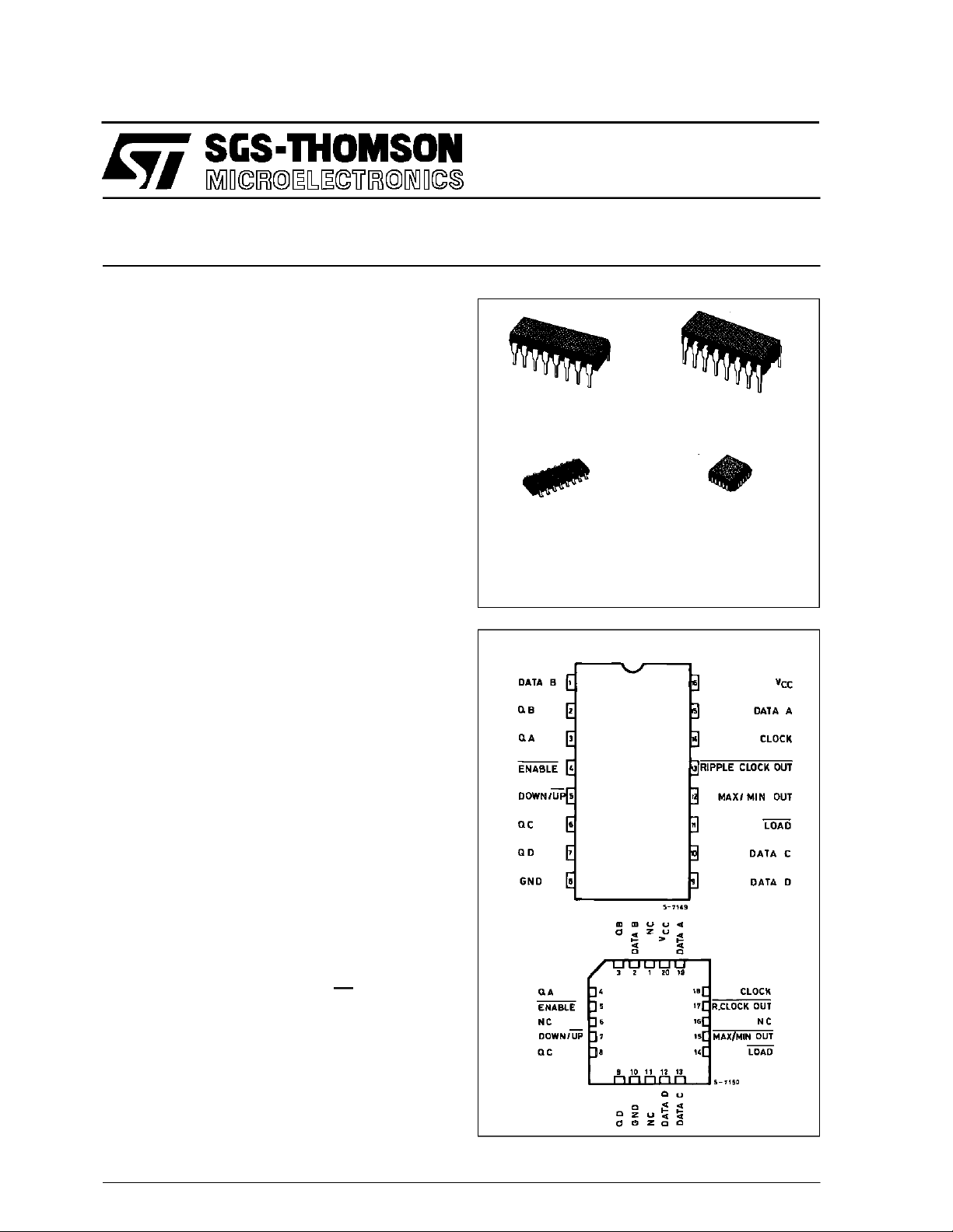
NC =
No Internal
Connection
PIN CONNECTIONS(top view)
October 1992
1/14
Page 2
M54/M74HC190/191
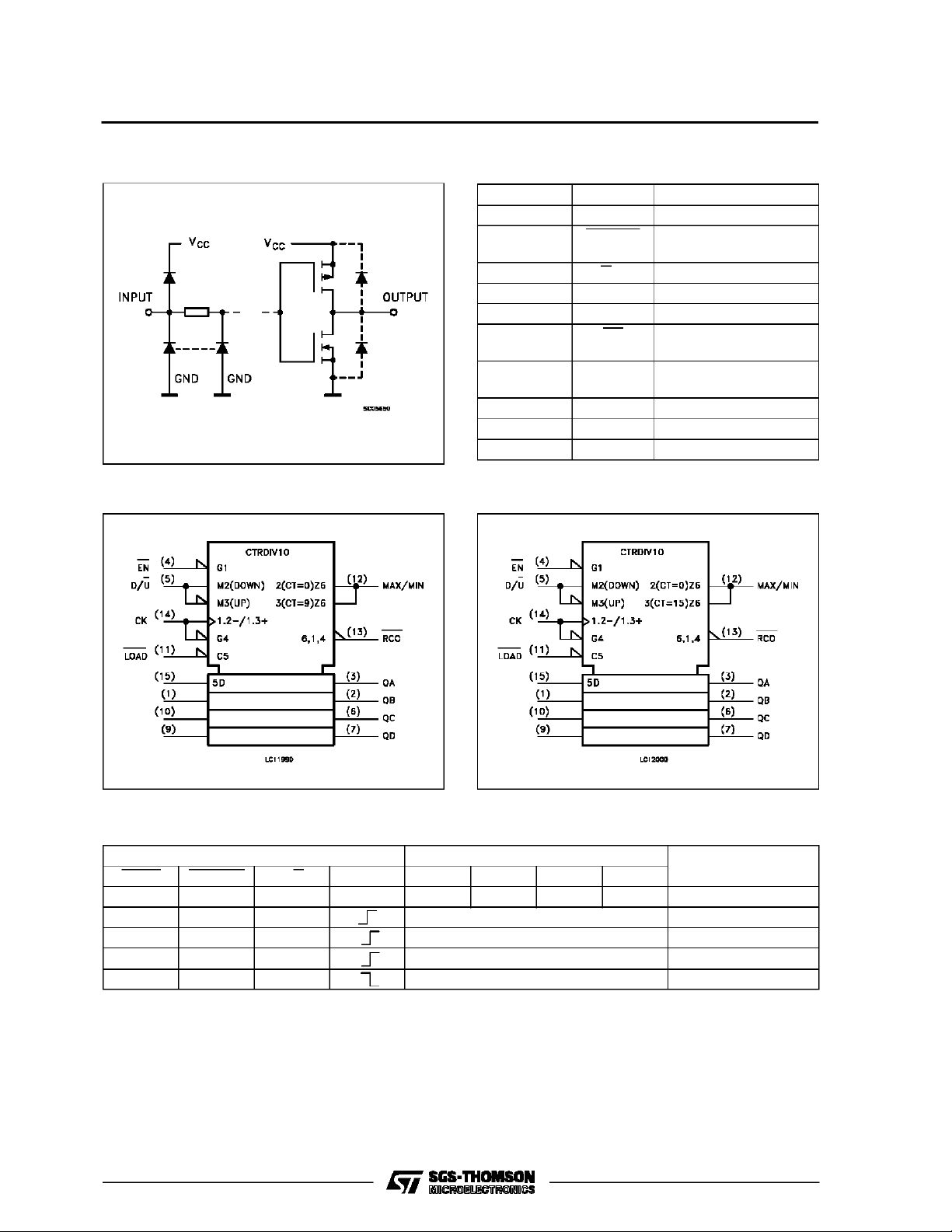
INPUT AND OUTPUT EQUIVALENT CIRCUIT
PIN DESCRIPTIO N
PIN No SYMBOL NAME AND FUNCTION
3, 2, 6, 7 QA to QD Flip-Flop Outputs
4 ENABLE Count Enable Input
(Active LOW)
5 U/D Parallel Data Input
11 LOAD Load Input (Active LOW)
12 MA/MI OUT Terminal Count Output
13 RC Ripple Clock Output
(Active LOW)
14 CLOCK Cloack Input (LOW to
HIGH, Edge-triggered)
15, 1, 10, 9 DA to DD Data Inputs
8 GND Ground (0V)
16 V
CC
Positive Supply Voltage
IEC LOGIC SYMBOL (HC191)IEC LOGIC SYMBOL (HC190)
TRUTH TABLE
INPUTS OUTPUS
LOAD ENABLE D/U CLOCK QA QB QC QD
L X X X a b c d PRESET DATA
H L L UP COUNT UP COUNT
H L H DOWN COUNT DOWN COUNT
H H X NO CHANGE NO COUNT
H X X NO CHANGE NO COUNT
X: Don’t Care
a -d: Thelevel of steadystate inputs atinputs a through Drespectively
2/14
FUNCTION
Page 3
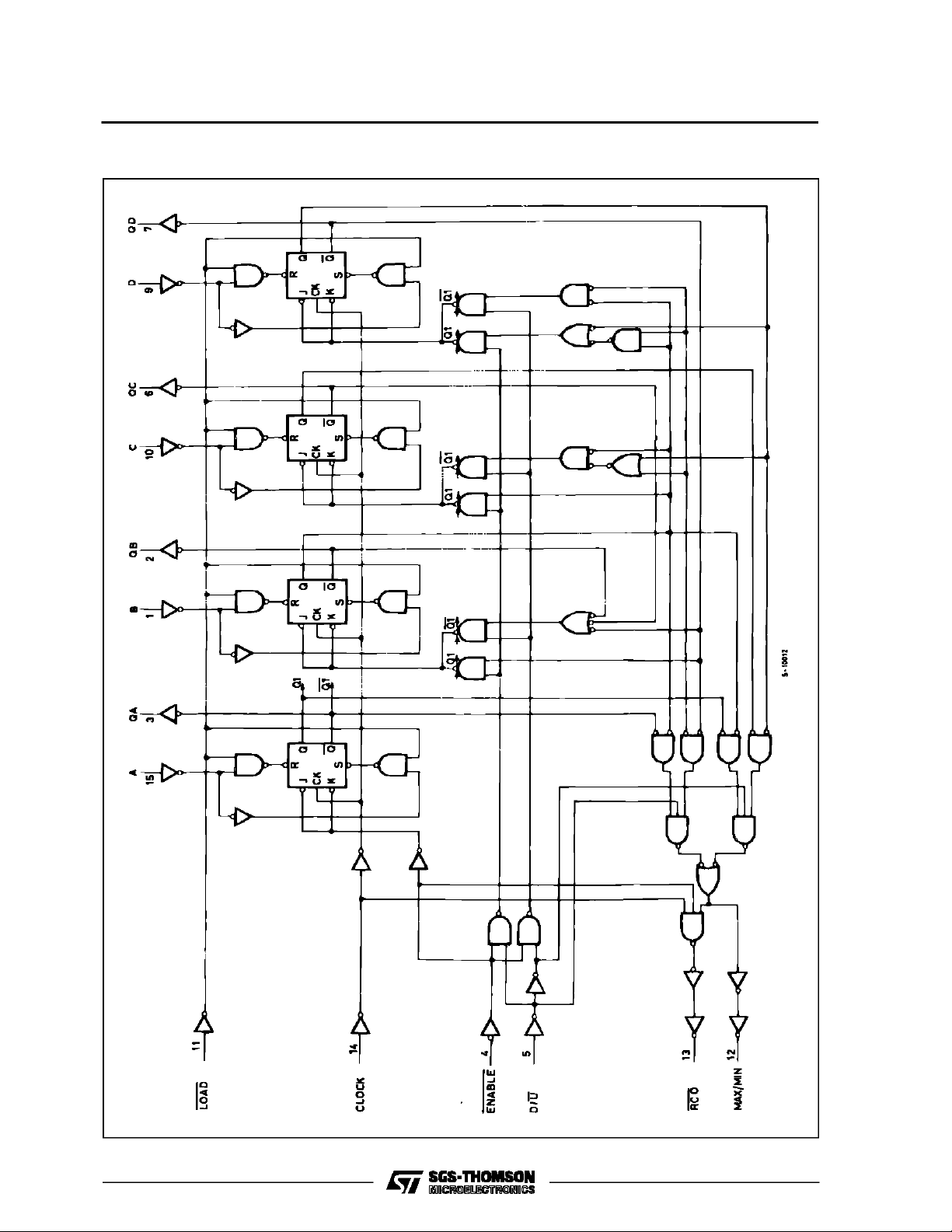
LOGIC DIAGRAM (HC190)
M54/M74HC190/191
3/14
Page 4
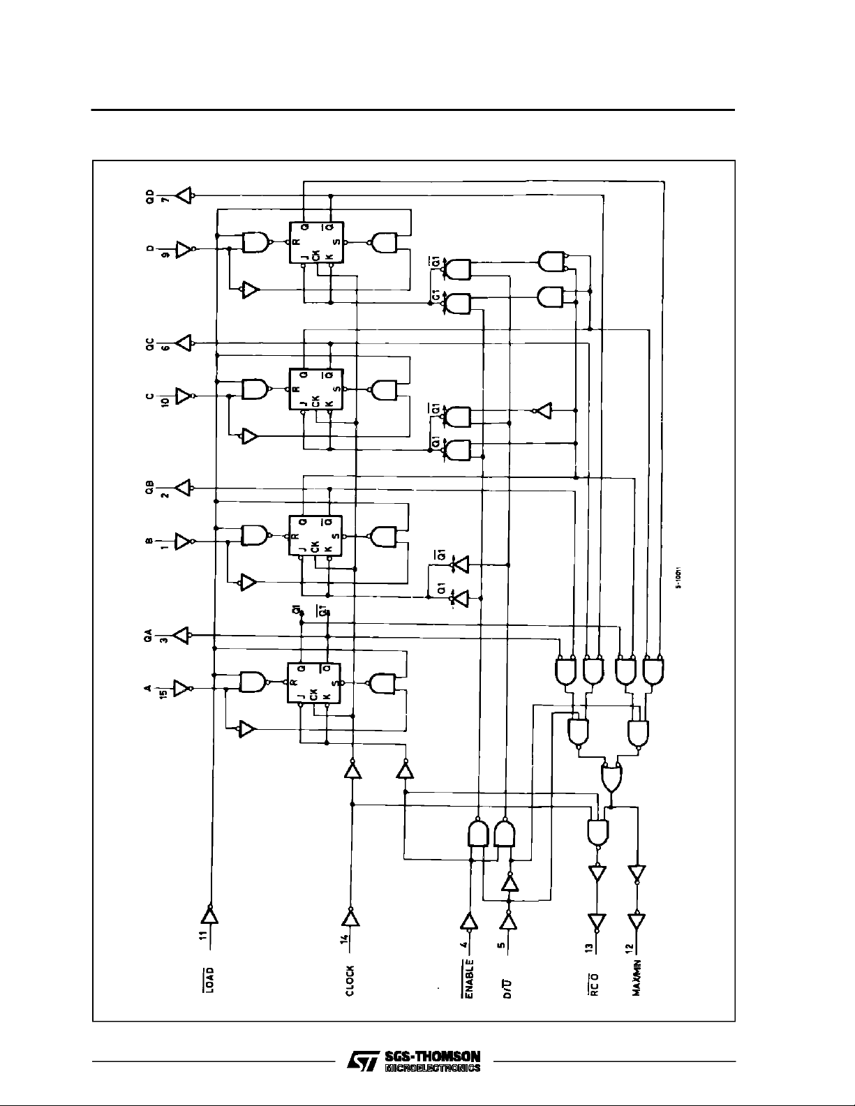
M54/M74HC190/191
LOGIC DIAGRAM (HC191)
4/14
Page 5
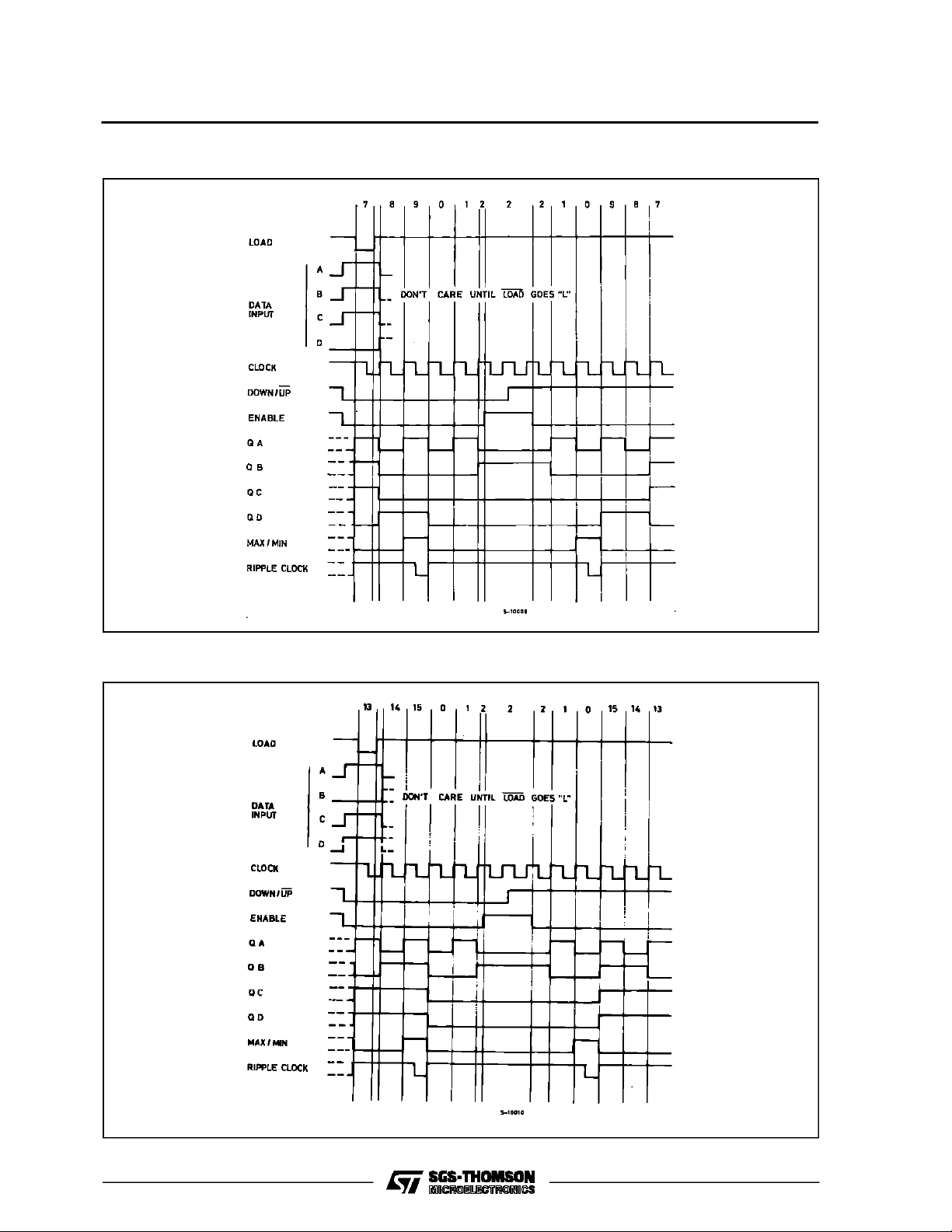
TIMING CHART (HC190)
M54/M74HC190/191
TIMING CHART (HC191)
5/14
Page 6

M54/M74HC190/191
ABSOLU TE MAXIMU M RAT INGS
Symbol Parameter Value Unit
V
CC
V
V
O
I
IK
I
OK
I
O
I
or I
CC
P
D
T
stg
T
AbsoluteMaximumRatings arethose values beyondwhichdamage tothedevicemayoccur. Functionaloperationunder theseconditionisnotimplied.
(*)500 mW: ≅ 65oC derateto 300 mWby 10mW/oC: 65oCto85oC
RECO MM ENDED OPERATING CONDI TI O NS
Symbol Parameter Value Unit
V
CC
V
I
V
O
T
op
t
r,tf
Supply Voltage -0.5 to +7 V
DC Input Voltage -0.5 to VCC+ 0.5 V
I
DC Output Voltage -0.5 to VCC+ 0.5 V
DC Input Diode Current ± 20 mA
DC Output Diode Current ± 20 mA
DC Output Source Sink CurrentPer OutputPin ± 25 mA
DC VCCor Ground Current ± 50 mA
GND
Power Dissipation 500 (*) mW
Storage Temperature -65 to +150
Lead Temperature (10 sec) 300
L
Supply Voltage 2 to 6 V
Input Voltage 0 to V
Output Voltage 0 to V
Operating Temperature: M54HC Series
M74HC Series
CC
CC
-55 to +125
-40 to +85
Input Rise and Fall Time VCC= 2 V 0 to 1000 ns
V
= 4.5 V 0 to 500
CC
V
= 6 V 0 to 400
CC
o
C
o
C
V
V
o
C
o
C
6/14
Page 7

DC SPECIFICA TIONS
Symbol Parameter
V
V
V
V
I
High Level Input
IH
Voltage
Low Level Input
IL
Voltage
High Level
OH
Output Voltage
Low Level Output
OL
Voltage
I
Input Leakage
I
Current
Quiescent Supply
CC
Current
M54/M74HC190/191
Test Conditions Value
T
=25oC
V
(V)
CC
A
54HC and 74HC
Min. Typ. Max. Min. Max. Min. Max.
2.0 1.5 1.5 1.5
4.5 3.15 3.15 3.15
6.0 4.2 4.2 4.2
2.0 0.5 0.5 0.5
4.5 1.35 1.35 1.35
6.0 1.8 1.8 1.8
2.0
4.5 4.4 4.5 4.4 4.4
6.0 5.9 6.0 5.9 5.9
4.5 I
6.0 I
2.0
4.5 0.0 0.1 0.1 0.1
6.0 0.0 0.1 0.1 0.1
4.5 I
6.0 I
6.0
=
V
I
IO=-20 µA
V
IH
or
V
IL
=-4.0 mA 4.18 4.31 4.13 4.10
O
=-5.2 mA 5.68 5.8 5.63 5.60
O
V
=
I
IO=20µA
V
IH
or
V
IL
= 4.0 mA 0.17 0.26 0.33 0.40
O
= 5.2 mA 0.18 0.26 0.33 0.40
O
VI=VCCor GND ±0.1 ±1 ±1 µA
1.9 2.0 1.9 1.9
0.0 0.1 0.1 0.1
6.0 VI=VCCor GND 4 40 80 µA
-40 to 85oC
74HC
-55 to 125oC
54HC
Unit
V
V
V
V
AC ELECTRICAL CHARACTERISTICS (CL=50pF,Inputtr=tf=6ns)
Test Conditions Value
Symbol Parameter
t
TLH
t
THL
t
PLH
t
PHL
Output Transition
Time
Propagation
Delay Time
(CLOCK - Q)
t
t
PLH
PHL
Propagation
Delay Time
(CLOCK - RCO)
t
t
PLH
PHL
Propagation Delay
Time (CLOCK MAX/MIN)
t
t
PLH
PHL
Propagation
Delay Time
(LOAD - Q)
=25oC
T
V
(V)
CC
A
54HC and 74HC
Min. Typ. Max. Min. Max. Min. Max.
2.0 30 75 95 110
4.5 8151922
6.0 7131619
2.0 92 180 225 270
4.5 23 36 45 54
6.0 20 31 38 46
2.0 39 120 150 180 ns
4.5 13 24 30 36
6.0 11 20 26 31
2.0 120 240 300 360 ns
4.5 30 48 60 72
6.0 26 41 51 61
2.0 108 205 255 310 ns
4.5 27 41 51 62
6.0 23 35 43 53
-40 to 85oC
74HC
-55 to 125oC
54HC
Unit
ns
ns
7/14
Page 8

M54/M74HC190/191
AC ELECTRICAL CHARACTERISTICS (CL=50pF,Inputtr=tf=6ns)
Test Conditions Value
T
=25oC
Symbol Parameter
t
t
PLH
PHL
Propagation
Delay Time
(DATA - Q)
t
t
PLH
PHL
Propagation
Delay Time
(ENABLE - RCO)
t
t
PLH
PHL
Propagation
Delay Time
(D/U - RCO)
t
t
PLH
PHL
Propagation
Delay Time
(D/U - MAX/MIN)
f
MAX
Maximum Clock
Frequency
V
CC
(V)
2.0 84 175 220 265
4.5 21 35 44 53
6.0 18 30 37 45
2.0 39 105 130 160
4.5 13 21 26 32
6.0 11 18 22 27
2.0 63 180 225 270
4.5 21 36 45 54
6.0 18 31 38 46
2.0 64 160 200 240
4.5 18 32 40 48
6.0 15 27 34 41
2.0 5 9 4 3.4
4.5 25 37 20 17
A
54HC and 74HC
Min. Typ. Max. Min. Max. Min. Max.
6.0 30 44 24 20
t
W(H)
t
W(L)
t
W(L)
Minimum Pulse
Width
(CLOCK)
Minimum Pulse
Width
(LOAD)
Minimum Set-up
t
s
Time
(SI, PI - CK)
Minimum Set-up
t
s
Time
(S0, S1 - CK)
Minimum Hold
t
h
Time
2.0 40 100 125 150
4.5 10 20 25 30
6.0 9172126
2.0 36 75 95 110
4.5 9151922
6.0 8131619
2.0 80 175 220 265
4.5 20 35 44 53
6.0 17 30 37 45
2.0 16 50 60 75
4.5 4101215
6.0 3 9 11 13
2.0 0 0 0
4.5 0 0 0
6.0 0 0 0
t
REM
Minimum
Removal Time
2.0 12 50 60 5
4.5 3101215
6.0 3 9 11 13
C
C
PD
(*) CPDisdefined as the value ofthe IC’sinternal equivalent capacitance which iscalculated from the operatingcurrent consumption without load.
(Referto Test Circuit). Average operting current canbe obtained by thefollowingequation. ICC(opr) = CPD•VCC•fIN+I
Input Capacitance 5 10 10 10 pF
IN
(*) Power Dissipation
Capacitance
for HC190
for HC191
111
112
-40 to 85oC
74HC
-55 to 125oC
54HC
CC
Unit
ns
ns
ns
ns
MHz
ns
ns
ns
ns
ns
ns
pF
8/14
Page 9

SWITCHING CHARACTERISTICS TEST WAVEFORM
M54/M74HC190/191
TEST CIRCUIT ICC(Opr.)
INPUT TRANSITIONTIME ISTHESAME AS THATIN CASE OF SWITCHINGCHARACTERISTICSTEST.
9/14
Page 10

M54/M74HC190/191
Plastic DIP16 (0.25) MECHANICAL DATA
DIM.
MIN. TYP. MAX. MIN. TYP. MAX.
a1 0.51 0.020
B 0.77 1.65 0.030 0.065
b 0.5 0.020
b1 0.25 0.010
D 20 0.787
E 8.5 0.335
e 2.54 0.100
e3 17.78 0.700
F 7.1 0.280
I 5.1 0.201
L 3.3 0.130
Z 1.27 0.050
mm inch
10/14
P001C
Page 11

Ceramic DIP16/1 MECHANICAL DATA
M54/M74HC190/191
DIM.
MIN. TYP. MAX. MIN. TYP. MAX.
A 20 0.787
B 7 0.276
D 3.3 0.130
E 0.38 0.015
e3 17.78 0.700
F 2.29 2.79 0.090 0.110
G 0.4 0.55 0.016 0.022
H 1.17 1.52 0.046 0.060
L 0.22 0.31 0.009 0.012
M 0.51 1.27 0.020 0.050
N 10.3 0.406
P 7.8 8.05 0.307 0.317
Q 5.08 0.200
mm inch
P053D
11/14
Page 12

M54/M74HC190/191
SO16 (Narrow) MECHANICAL DATA
DIM.
MIN. TYP. MAX. MIN. TYP. MAX.
A 1.75 0.068
a1 0.1 0.2 0.004 0.007
a2 1.65 0.064
b 0.35 0.46 0.013 0.018
b1 0.19 0.25 0.007 0.010
C 0.5 0.019
c1 45° (typ.)
D 9.8 10 0.385 0.393
E 5.8 6.2 0.228 0.244
e 1.27 0.050
e3 8.89 0.350
F 3.8 4.0 0.149 0.157
G 4.6 5.3 0.181 0.208
L 0.5 1.27 0.019 0.050
M 0.62 0.024
S8°(max.)
mm inch
12/14
P013H
Page 13

PLCC20 MECHANICAL DATA
M54/M74HC190/191
DIM.
MIN. TYP. MAX. MIN. TYP. MAX.
A 9.78 10.03 0.385 0.395
B 8.89 9.04 0.350 0.356
D 4.2 4.57 0.165 0.180
d1 2.54 0.100
d2 0.56 0.022
E 7.37 8.38 0.290 0.330
e 1.27 0.050
e3 5.08 0.200
F 0.38 0.015
G 0.101 0.004
M 1.27 0.050
M1 1.14 0.045
mm inch
P027A
13/14
Page 14

M54/M74HC190/191
Information furnishedis believed to be accurate and reliable.However, SGS-THOMSON Microelectronics assumes no responsabilityfor the
consequences of useof such information norfor any infringementof patents or other rights of third parties which may results from its use. No
license is granted byimplication or otherwiseunderany patentor patent rights ofSGS-THOMSON Microelectronics.Specificationsmentioned
in thispublication are subjectto change without notice.This publication supersedes and replaces all information previouslysupplied.
SGS-THOMSON Microelectronicsproducts are not authorized foruse ascritical componentsinlife supportdevices or systemswithoutexpress
written approval ofSGS-THOMSON Microelectonics.
1994SGS-THOMSON Microelectronics- All Rights Reserved
Australia -Brazil - France- Germany- HongKong - Italy- Japan - Korea - Malaysia- Malta - Morocco -The Netherlands-
Singapore -Spain - Sweden - Switzerland -Taiwan -Thailand - UnitedKingdom -U.S.A
SGS-THOMSON Microelectronics GROUP OFCOMPANIES
14/14
 Loading...