

Page 1
FUNCTION LOOK AHEAD CARRY GENERATOR
.HIGH SPEED
tPD= 14 ns(TYP.) at VCC=5V
.LOWPOWER DISSIPATION
ICC=4µA(MAX.) at TA=25°C
.HIGH NOISE IMMUNITY
V
NIH=VNIL
=28%VCC(MIN.)
.OUTPUT DRIVE CAPABILITY
10 LSTTL LOADS
.SYMMETRICAL OUTPUT IMPEDANCE
IOH =IOL= 4 mA(MIN.)
.BALANCEDPROPAGATION DELAYS
t
PLH=tPHL
.WIDE OPERATING VOLTAGE RANGE
VCC(OPR)= 2 V to 6 V
.PIN ANDFUNCTION COMPATIBLE
WITH 54/74LS182
DESCRIPTION
The M54/74HC182 is a high speed CMOS FUNCTION LOOK AHEAD CARRY GENERATOR
fabricated insilicongate C2MOStechnology. It has
the same high speed performance of LSTTL combined with true CMOS low power consumption.
These circuit are capable of anticipating a carry
acrossfour binary addersor group of adders. They
arecascadable to perform full look-ahead across nbit adders. Carry, generate-carry, and
propagate-carry functions are providedas shown in
the pinconnection table. When used in conjunction
with the HC181 arithmetic logic unit, these generators provide high-speed carry look-ahead
capability for any word length. Each HC182 generates the look-ahead (anticipated carry) across a
groupoffourALU’sand,inaddition, othercarrylookaheadcircuits may be employed toanticipate carry
across sections of four look-ahead packages up to
n-bits. Themethod of cascading circuits to perform
multi-levellook-ahead isillustrated under typical application data.
Carry input and outputof the ALUs are in their true
form, andthe carrypropagate (P) and carrygenerate (G) are in negated form ; therefore, the carry
functions(inputs, outputs,generate, andpropagate)
of the look-ahead generators are implemented in
the compatible forms for direct connection to the
ALU. Reinterpretation of carry functions as explained ontheHC181datasheetarealsoapplicable
toandcompatible withthelook-aheadgenerator. All
inputs areequipped with protection circuits against
staticdischarge and transient excess voltage.
M54HC182
M74HC182
B1R
(PlasticPackage)
M1R
(MicroPackage)
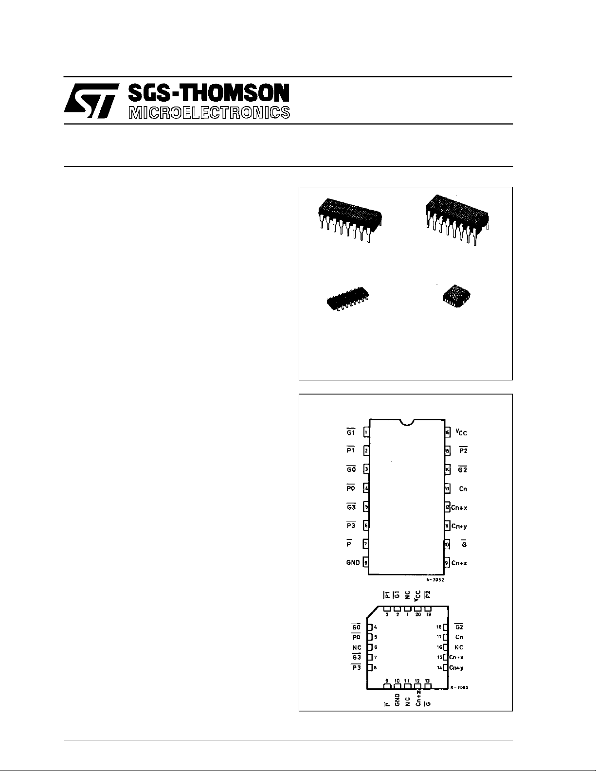
ORDER CODES :
M54HC 182F1R M74H C182M1R
M74HC 182B1R M74HC1 82C1R
PIN CONNECTIONS(top view)
NC =
No Internal
Connection
F1R
(CeramicPackage)
C1R
(Chip Carrier)
March1993
1/12
Page 2
M54/M74HC182
FUNCTION TABLES
FOR G OUTPUT
INPUTS OUTPUT
G3 G2 G1 G0 P3 P2 P1 G
LXXXXXXL
XLXXLXXL
XXLXLLXL
XXXLLLLL
ALL OTHER COMBINATIONS H
FOR P OUTPUT
INPUTS OUTPUT
P3 P2 P1 P0 P
LLLLL
ALL OTHER COMBINATIONS H
FOR Cn+x OU TPUT
INPUTS OUTPUT
G0 P0 Cn Cn+x
LXXH
XLHH
ALL OTHER COMBINATIONS L
FOR Cn+y OU TPUT
INPUTS OUTPUT
G1 G0 P1 P0 Cn Cn+y
LXXXXH
XLLXXH
XXLLHH
ALL OTHER COMBINATIONS L
FOR Cn+z OU TPUT
INPUTS OUTPUT
G2 G1 G0 P2 P1 P0 Cn Cn+z
LXXXXXXH
XLXLXXXH
XXLLLXXH
XXXLLLHH
ALL OTHER COMBINATIONS L
Cn+x = G0 + P0Cn
Cn+y = G1 + P1G0 + P1P0Cn
Cn+z = G2 + P2G1 + P2P1G0 + P2P1P0Cn
G = G3+ G3 + P3G2 + P3P2G1 + P3P2P1G0
P = P3P2P1P0
or
Cn+x = Y0 + (X0 + Cn)
Cn+y = Y1 + [X1+ Y0(X0+ Cn)]
Cn+z = Y2 + {X2 + Y1[X1 + Y0(X0+Cn)]}
G = Y3 + (X3 + Y2)(X3+ X2 + Y1)(X3 + X2 + X1 + Y0)
P = X3 + X2 + X1 + X0
2/12
Page 3
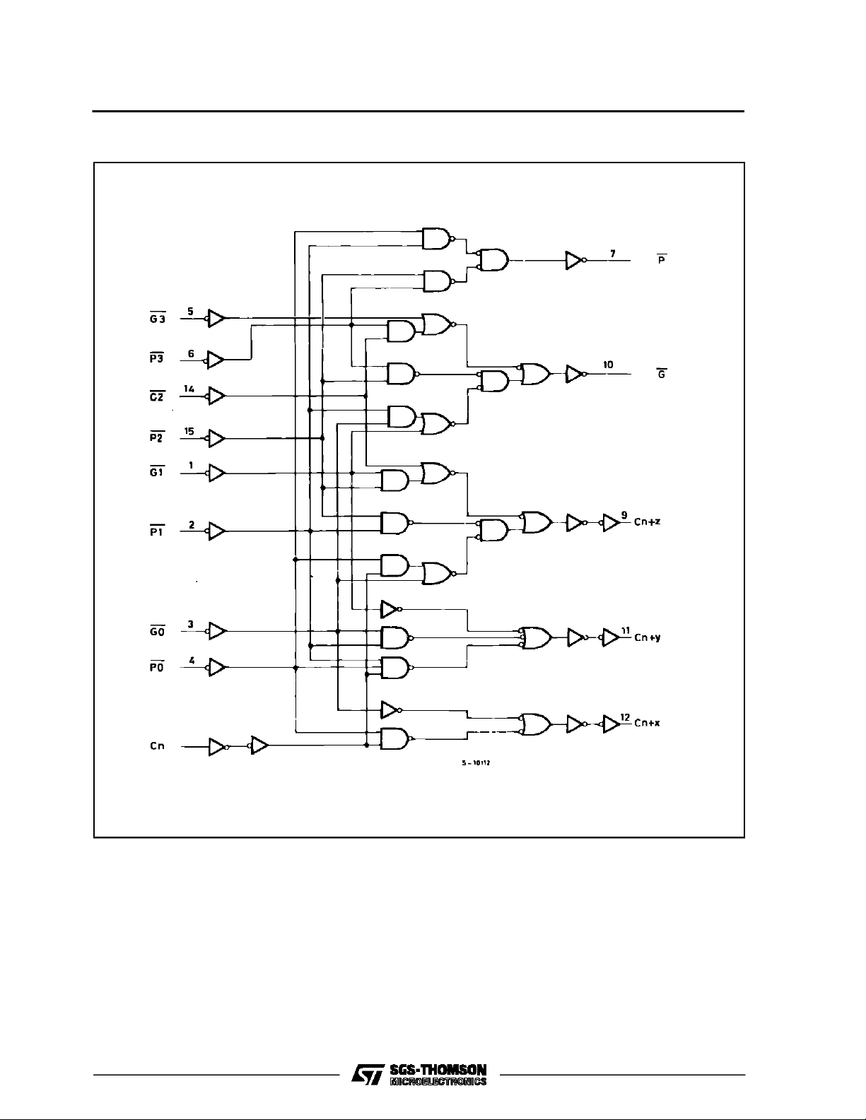
LOGIC DIAGRAM
M54/M74HC182
3/12
Page 4
M54/M74HC182
INPUT AND OUTPUT EQUIVALENT CIRCUIT PIN DESCRIPTION
PIN No SYMBOL NAME AND FUNCTION
3, 1, 14, 5 G0 to G3 Carry Generate Inputs
4, 2, 15, 6 P0 to P3 Carry Propagate Inputs
7 P Carry Propagate Output
9 Cn+z Function Output
10 G Carry Generate Output
11 Cn+y Function Output
12 Cn+x Function Output
13 Cn
8 GND Ground (0V)
16 V
IEC LOGIC SYMBOLS
CC
(Active LOW)
(Active LOW)
(Active LOW)
(Active LOW)
Positive Supply Voltage
ABSOLU TE MAXI MU M RAT INGS
Symbol Parameter Value Unit
V
CC
V
V
O
I
IK
I
OK
I
O
or I
I
CC
P
D
T
stg
T
AbsoluteMaximumRatings arethose valuesbeyond whichdamage tothedevice mayoccur. Functionaloperation under these conditionisnotimplied.
(*)500 mW:≅ 65oC derate to 300mW by 10mW/oC: 65oCto85oC
4/12
Supply Voltage -0.5 to +7 V
DC Input Voltage -0.5 to VCC+ 0.5 V
I
DC Output Voltage -0.5 to VCC+ 0.5 V
DC Input Diode Current ± 20 mA
DC Output Diode Current ± 20 mA
DC Output Source Sink Current Per Output Pin ± 25 mA
DC VCCor Ground Current ± 50 mA
GND
Power Dissipation 500 (*) mW
Storage Temperature -65 to +150
Lead Temperature (10 sec) 300
L
o
C
o
C
Page 5

M54/M74HC182
RECO MM ENDED OPERAT IN G CO NDI TI O NS
Symbol Parameter Value Unit
V
V
V
T
t
r,tf
DC SPECIFICATIONS
Symbol Parameter
V
IH
V
V
OH
V
OL
I
I
OZ
I
CC
Supply Voltage 2 to 6 V
CC
Input Voltage 0 to V
I
Output Voltage 0 to V
O
Operating Temperature: M54HC Series
op
M74HC Series
CC
CC
-55 to +125
-40 to +85
Input Rise and Fall Time VCC= 2 V 0 to 1000 ns
V
= 4.5 V 0 to 500
CC
V
= 6 V 0 to 400
CC
Test Conditions Value
V
(V)
CC
=25oC
T
A
54HC and 74HC
-40 to 85oC
74HC
-55 to 125oC
Min. Typ. Max. Min. Max. Min. Max.
High Level Input
Voltage
2.0 1.5 1.5 1.5
4.5 3.15 3.15 3.15
6.0 4.2 4.2 4.2
Low Level Input
IL
Voltage
2.0 0.5 0.5 0.5
4.5 1.35 1.35 1.35
6.0 1.8 1.8 1.8
High Level
Output Voltage
Low Level Output
Voltage
Input Leakage
I
Current
3 State Output
Off State Current
Quiescent Supply
2.0
V
=
I
4.5 4.4 4.5 4.4 4.4
6.0 5.9 6.0 5.9 5.9
4.5 I
6.0 I
2.0
4.5 0.0 0.1 0.1 0.1
6.0 0.0 0.1 0.1 0.1
4.5 I
6.0 I
6.0
IO=-20 µA
V
IH
or
V
IL
=-6.0 mA 4.18 4.31 4.13 4.10
O
=-7.8 mA 5.68 5.8 5.63 5.60
O
V
=
I
IO=20µA
V
IH
or
V
IL
= 6.0 mA 0.17 0.26 0.37 0.40
O
= 7.8 mA 0.18 0.26 0.37 0.40
O
VI=VCCor GND ±0.1 ±1 ±1 µA
6.0 VI=VIHor V
1.9 2.0 1.9 1.9
0.0 0.1 0.1 0.1
IL
±0.5 ±5.0 ±10 µA
VO=VCCor GND
6.0 VI=VCCor GND 4 40 80 µA
Current
54HC
V
V
o
C
o
C
Unit
V
V
V
V
5/12
Page 6

M54/M74HC182
AC ELECTRICAL CHARACTERISTICS (CL=50pF,Inputtr=tf=6ns)
Test Conditions Value
T
=25oC
Symbol Parameter
t
t
TLH
THL
Output Transition
Time
V
CC
(V)
2.0 30 75 95 110
4.5 8151922
A
54HC and 74HC
Min. Typ. Max. Min. Max. Min. Max.
6.0 7131619
t
PLH
t
PHL
Propagation
Delay Time
(Gn, Pn - Cn+xyz)
t
t
PLH
PHL
Propagation
Delay Time
(Gn, Pn - G)
t
t
PLH
PHL
Propagation
Delay Time
(Pn - P)
t
t
PLH
PHL
Propagation
Delay Time
(Cn - Cn+xyz)
C
C
PD
Input Capacitance 5 10 10 10 pF
IN
(*) Power Dissipation
2.0 62 135 170 205
4.5 17 27 34 41
6.0 13 23 29 35
2.0 72 150 190 225
4.5 19 30 38 45
6.0 14 26 32 38
2.0 62 135 170 205
4.5 17 27 34 41
6.0 13 23 29 35
2.0 62 135 170 205
4.5 17 27 34 41
6.0 13 23 29 35
61
Capacitance
(*) CPDisdefined as the valueof the IC’s internal equivalent capacitance whichis calculated fromthe operating current consumption withoutload.
(RefertoTest Circuit).Average opertingcurrent can be obtained by the followingequation. ICC(opr) = CPD•VCC•fIN+ICC/2(per FLIP/FLOP)
-40 to 85oC
74HC
-55 to 125oC
54HC
Unit
ns
ns
ns
ns
ns
pF
6/12
Page 7

SWITCHING CHARACTERISTICS TEST WAVEFORM
TEST CIRCUIT ICC(Opr.)
M54/M74HC182
INPUT WAVEFORM IS THE SAME AS THAT IN CASE OF SWITCHING CHARACTERISTICS TEST.
TYPICAL APPLICATION
64-BIT ALU, FULL-CARRY LOOK-AHEAD IN THREE LEVELS.
7/12
Page 8

M54/M74HC182
Plastic DIP16 (0.25) MECHANICAL DATA
DIM.
MIN. TYP. MAX. MIN. TYP. MAX.
a1 0.51 0.020
B 0.77 1.65 0.030 0.065
b 0.5 0.020
b1 0.25 0.010
D 20 0.787
E 8.5 0.335
e 2.54 0.100
e3 17.78 0.700
F 7.1 0.280
I 5.1 0.201
L 3.3 0.130
Z 1.27 0.050
mm inch
8/12
P001C
Page 9

Ceramic DIP16/1 MECHANICAL DATA
M54/M74HC182
DIM.
MIN. TYP. MAX. MIN. TYP. MAX.
A 20 0.787
B 7 0.276
D 3.3 0.130
E 0.38 0.015
e3 17.78 0.700
F 2.29 2.79 0.090 0.110
G 0.4 0.55 0.016 0.022
H 1.17 1.52 0.046 0.060
L 0.22 0.31 0.009 0.012
M 0.51 1.27 0.020 0.050
N 10.3 0.406
P 7.8 8.05 0.307 0.317
Q 5.08 0.200
mm inch
P053D
9/12
Page 10

M54/M74HC182
SO16 (Narrow) MECHANICAL DATA
DIM.
MIN. TYP. MAX. MIN. TYP. MAX.
A 1.75 0.068
a1 0.1 0.2 0.004 0.007
a2 1.65 0.064
b 0.35 0.46 0.013 0.018
b1 0.19 0.25 0.007 0.010
C 0.5 0.019
c1 45° (typ.)
D 9.8 10 0.385 0.393
E 5.8 6.2 0.228 0.244
e 1.27 0.050
e3 8.89 0.350
F 3.8 4.0 0.149 0.157
G 4.6 5.3 0.181 0.208
L 0.5 1.27 0.019 0.050
M 0.62 0.024
S8°(max.)
mm inch
10/12
P013H
Page 11

PLCC20 MECHANICAL DATA
M54/M74HC182
DIM.
MIN. TYP. MAX. MIN. TYP. MAX.
A 9.78 10.03 0.385 0.395
B 8.89 9.04 0.350 0.356
D 4.2 4.57 0.165 0.180
d1 2.54 0.100
d2 0.56 0.022
E 7.37 8.38 0.290 0.330
e 1.27 0.050
e3 5.08 0.200
F 0.38 0.015
G 0.101 0.004
M 1.27 0.050
M1 1.14 0.045
mm inch
P027A
11/12
Page 12

M54/M74HC182
Information furnished is believed to be accurate and reliable.However, SGS-THOMSON Microelectronics assumes no responsability forthe
consequences of use of such information nor for any infringement of patents or other rightsof third parties which mayresults from its use. No
license isgranted by implication orotherwise underany patentor patentrights of SGS-THOMSON Microelectronics. Specificationsmentioned
in this publication are subject to changewithout notice.This publication supersedes andreplaces all information previously supplied.
SGS-THOMSON Microelectronicsproducts are notauthorizedforuse ascritical componentsin life support devicesor systemswithout express
written approval of SGS-THOMSON Microelectonics.
1994 SGS-THOMSON Microelectronics- All RightsReserved
Australia - Brazil - France- Germany - Hong Kong - Italy- Japan - Korea - Malaysia - Malta - Morocco - The Netherlands -
Singapore - Spain - Sweden- Switzerland -Taiwan - Thailand- UnitedKingdom - U.S.A
SGS-THOMSON Microelectronics GROUP OF COMPANIES
12/12
 Loading...