

Page 1
ARITHMETIC LOGIC UNIT/FUNCTION GENERATOR
.HIGH SPEED
tPD= 13 ns(TYP.) AT VCC=5V
.LOWPOWER DISSIPATION
ICC=4µA(MAX.) at TA=25°C
.HIGH NOISE IMMUNITY
V
NIH=VNIL
=28%VCC(MIN.)
.OUTPUTDRIVE CAPABILITY
10 LSTTL LOADS
.SYMMETRICAL OUTPUT IMPEDANCE
IOH =IOL= 4 mA (MIN.)
.BALANCEDPROPAGATIONDELAYS
t
PLH=tPHL
.WIDE OPERATING VOLTAGE RANGE
VCC(OPR)= 2 V to 6 V
.PIN AND FUNCTION COMPATIBLE
WITH 54/74LS181
DESCRIPTION
The74HC181 is a high speed CMOSARITHMETIC
LOGIC UNIT/FUNCTION GENERATOR fabricated
withsilicongateC2MOStechnology. It has the same
highspeedperformanceofLSTTLcombinedwithtrue
CMOS low power consumption. These circuits perform 16 binary arithmetic operations on two 4-bit
words as shown intables 1 and2. These operations
areselectedby the fourfunction-select lines (S0, S1,
S2,S3) andinclude addition, subtraction, decrement,
and straight transfer. When performing arithmetic
manipulations, theinternal carriesmustbeenabled by
applying a low-levelvoltage to themode control input
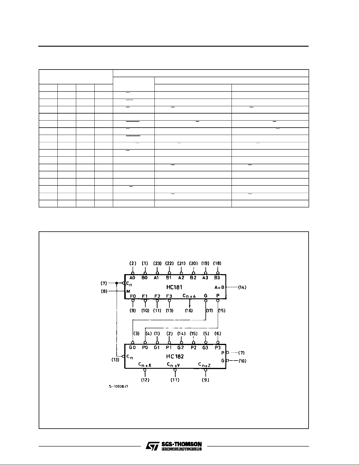
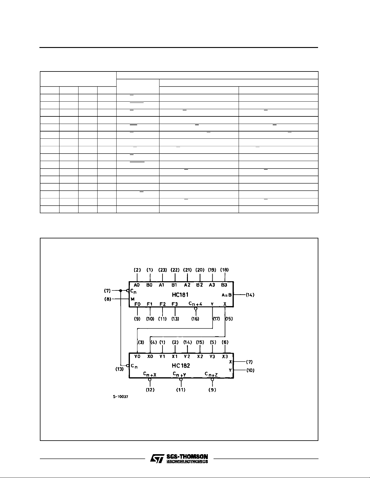
(M).Afullcarrylook-ahead schemeismadeavailable
in these devices for fast, simultaneous carry generationby meansof two cascade-outputs (pins15 and
17)forthefourbitsinthepackage. Whenusedinconjunction withthe M54HC182 orM74HC182, full carry
look-ahead circuits,high-speed arithmetic operations
canbeperformed. These circuits willaccomodate active-highoractive-lowdata,ifthepindesignations are
interpreted as shown below. Subtraction is accomplished by 1,s complement addition where the 1’s
complement ofthesubtrahendisgenerated internally.
Theresultant output is1–B–1, whichrequires anendaround or forced carry to produce A–B.The181can
alsobeutilized as a comparator. The A = B outputis
internally decoded fromthe functionoutputs (F0, F1,
F2, F3) so thatwhen two words of equal magnitude
areappliedattheAandB inputs, itwillassumeahigh
level toindicated equality (A =B).TheALUshould be
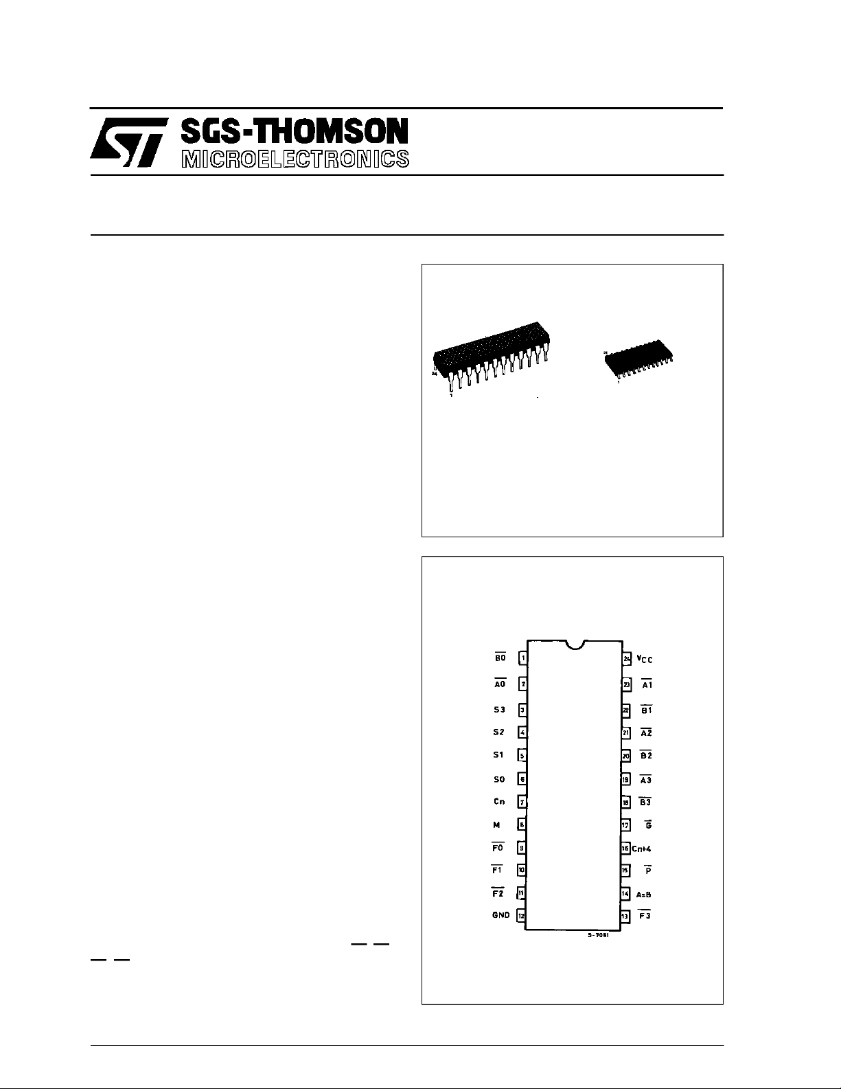
M74HC181
B1R
(Plastic Package)
ORDER CODES :
M74HC 181M1R M74HC 181B1R
PIN CONNECTIONS(top view)
* Open drain OutputStructure
M1R
(MicroPackage)
October 1993
1/13
Page 2
M74HC181
DESCRIPTION (continued)
inthesubtractmodewithCn=Hwhenperforming this
comparison. The A =B output isopen-drain sothat it
canbe wire-AND connected togiveacomparison for
morethatfourbits. Thecarry output (Cn+4) canalso
be used to supply relative magnitude information.
Again,theALUshould beplacedinthesubtractmode
byplacing thefunction selectinputsS3,S2, S1,S0at
L,H, H, L, respectively. These circuits have beendesigned to notonlyincorporate allofthedesigner’s re-
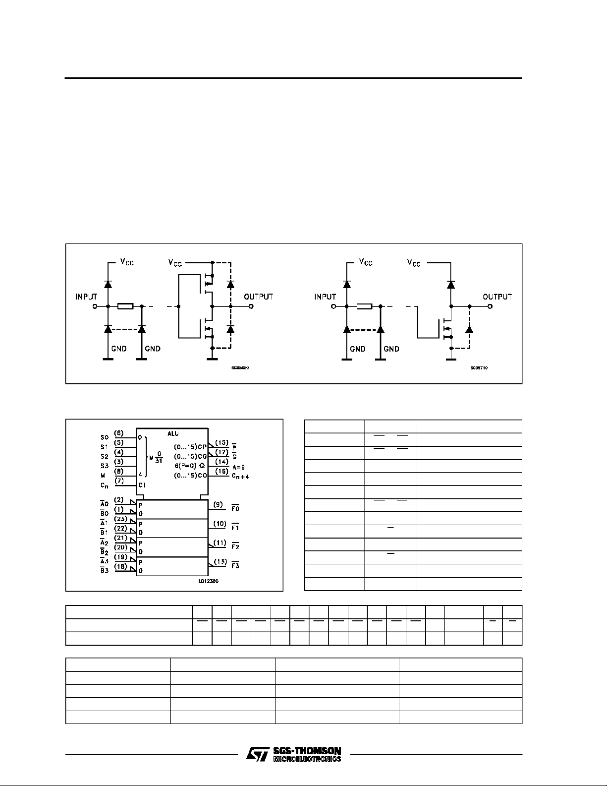
INPUT AND OUTPUT EQUIVALENT CIRCUITS
quirements for arithmetic operations, but also to provide 16 possible functions of two Boolean variables
withouttheuse ofexternalcircuitry.These logic functionsareselectedbyuseofthefourfunction-selectinputs(S0,S1, S2,S3) withthemode-control input (M)
atahighlevel to disable the internal carry.Allinputs
areequipped withprotectioncircuitsagainst staticdischarge and transient excessvoltage.
ONLY OUTPUT A = B
IEC LOGIC SYMBOLS
PIN NUMBER 2 1 23 22 21 20 19 18 9 10 11 13 7 16 15 17
ACTIVE LOW DATA (Table 1) A0 B0 A1 B1 A2 B2 A3 B3 F0 F1 F2 F3 Cn Cn + 4 P G
ACTIVE HIGH DATA (Table 1) A0 B0 A1 B1 A2 B2 A3 B3 F0 F1 F2 F3 Cn Cn + 4 X Y
PIN DESCRIPTI ON
PIN No SYMBOL NAME AND FUNCTION
2, 23, 21, 19 A0 to A3 Word A Inputs
1, 22, 20, 18 B0 to B3 Word B Inputs
6, 5, 4, 3 S0 to S3 Function Select Inputs
7 Cn Inv. Carry Input
8 M Mode Control Input
9, 10, 11, 13 F0 to F3 Function Outputs
14 A = B Comparator Output
15 P Carry Propagate Output
16 Cn + 4 Inv. Carry Output
17 G Carry Generate Output
12 GND Ground (0V)
24 V
CC
Positive Supply Voltage
2/13
Input Cn Output Cn + 4 Active LOW Data (Figure 1) Active HIGH Data (Figure 2)
HHA≥BA≤B
HLA<BA>B
LHA>BA<B
LLA≤BA≥B
Page 3
TRUTH TABLE 1
M74HC181
Selection
S3 S2 S1 S0 Cn = L (no carry) Cn = H (with carry)
L L L L F = A F = A Minus 1 F = A
L L L H F = AB F = AB Minus 1 F = AB
L L H L F = A + B F = AB Minus 1 F = (AB)
L L H H F = 1 F = Minus 1 (2’s Compl) F = Zero
L H L L F=A+B F=APlus (A + B) F = A Plus (A + B) Plus 1
L H L H F = B F = AB Plus (A + B) F = AB Plus (A + B) Plus 1
LHHLF=A⊕B F = A Minus B Minus 1 F = A Minus B
L H H H F=A+B F=A+B F=(A+B)Plus 1
H L L L F = AB F = A Plus (A + B) F = A Plus (A + B) Plus 1
HLLHF=A⊕B F = A Plus B F = A Plus B Plus 1
H L H L F = B F = AB Plus (A + B) F = AB Plus (A + B) Plus 1
H L H H F=A+B F=A+B F=(A+B)Plus 1
H H L L F = 0 F = A Plus A * F = A Plus A Plus 1
H H L H F = AB F = AB Plus A F = AB Plus A Plus 1
H H H L F = AB F = AB Plus A F = AB Plus A Plus 1
H H H H F = A F = A F = A Plus 1
* Eachbit is shiftedto the nextmore significantposition.
M = H Logic
Functions
ACTIVE LOW DATA
M = L: Arithmetic Operations
FIGURE 1
3/13
Page 4
M74HC181
TRUTH TABLE 2
Selection
S3 S2 S1 S0 Cn = H (no carry) Cn = L (with carry)
L L L L F = A F = A F = A Plus 1
L L L H F=A+B F=A+B F=(A+B)Plus 1
L L H L F=AB F=A+B F=(A+B)Plus 1
L L H H F = 0 F = Minus 1 (2’s Compl) F = Zero
L H L L F = AB F = A Plus (AB) F = A Plus AB Plus 1
L H L H F = B F = (A + B) Plus AB F = (A + B) Plus (AB) Plus 1
LHHLF=A⊕B F = A Minus B Minus 1 F = A Minus B
L H H H F = AB F = AB Minus 1 F = AB
H L L L F = A + B F = A Plus AB F = A Plus AB Plus 1
HLLHF=A⊕B F = A Plus B F = A Plus B Plus 1
H L H L F = B F = (A + B) Plus AB F = (A + B) Plus AB Plus 1
H L H H F = AB F = AB Minus 1 F = AB
H H L L F = 1 F = A Plus A * F = A Plus A Plus 1
H H L H F = A + B F = (A + B) Plus A F = (A + B) Plus A Plus 1
H H H L F = A + B F = (A + B) Plus A F = (A + B) Plus A Plus 1
H H H H F = A F = A Minus 1 F = A
* Eachbit is shiftedto the nextmore significantposition.
M = H Logic
Functions
ACTIVE HIGH DATA
M = L: Arithmetic Operations
FIGURE 2
4/13
Page 5

LOGIC DIAGRAM
M74HC181
5/13
Page 6

M74HC181
ABSOLU TE M AXIMU M R AT INGS
Symbol Parameter Value Unit
V
CC
V
V
O
I
IK
I
OK
I
O
I
or I
CC
P
D
T
stg
T
AbsoluteMaximumRatingsarethosevalues beyond whichdamage tothedevice mayoccur. Functional operationundertheseconditionisnotimplied.
(*)500 mW:≅ 65oC derate to 300mW by 10mW/oC: 65oCto85oC
RECO MM ENDED OPERAT IN G CO NDITIO NS
Symbol Parameter Value Unit
V
CC
V
I
V
O
T
op
t
r,tf
Supply Voltage -0.5 to +7 V
DC Input Voltage -0.5 to VCC+ 0.5 V
I
DC Output Voltage -0.5 to VCC+ 0.5 V
DC Input Diode Current ± 20 mA
DC Output Diode Current ± 20 mA
DC Output Source Sink Current Per Output Pin ± 25 mA
DC VCCor Ground Current ± 50 mA
GND
Power Dissipation 500 (*) mW
Storage Temperature -65 to +150
Lead Temperature (10sec) 300
L
Supply Voltage 2 to 6 V
Input Voltage 0 to V
Output Voltage 0 to V
CC
CC
Operating Temperature -40 to +85
Input Rise and Fall Time VCC= 2 V 0 to 1000 ns
V
= 4.5 V 0 to 500
CC
= 6 V 0 to 400
V
CC
o
C
o
C
V
V
o
C
6/13
Page 7

DC SPECIFICATIONS
Symbol Parameter
V
V
V
V
I
High Level Input Voltage 2.0 1.5 1.5
IH
Low Level Input
IL
Voltage
High Level Output Voltage
OH
(except A = B output)
Low Level Output Voltage 2.0
OL
Input Leakage Current 6.0 VI=VCCor GND ±0.1 ±1 µA
I
I
Quiescent Supply Current 6.0 VI=VCCor GND 4 40 µA
CC
M74HC181
Test Conditions Value
V
CC
(V)
4.5 3.15 3.15
6.0 4.2 4.2
2.0 0.5 0.5
4.5 1.35 1.35
6.0 1.8 1.8
2.0
4.5 4.4 4.5 4.4
6.0 5.9 6.0 5.9
4.5 I
6.0 I
4.5 0.0 0.1 0.1
6.0 0.0 0.1 0.1
4.5 I
6.0 I
V
I
V
IH
or
V
IL
V
I
V
IH
or
V
IL
=
IO=-20 µA
=-4.0 mA 4.18 4.31 4.13
O
=-5.2 mA 5.68 5.8 5.63
O
=
IO=20µA
= 4.0 mA 0.17 0.26 0.33
O
= 5.2 mA 0.18 0.26 0.33
O
TA=25oC -40 to 85oC
Min. Typ. Max. Min. Max.
1.9 2.0 1.9
0.0 0.1 0.1
Unit
V
V
V
V
7/13
Page 8

M74HC181
AC ELECTRICAL CHARACTERISTICS (CL=50pF,Inputtr=tf=6ns)
Test Conditions Value
=25oC
T
Symbol Parameter
t
t
TLH
THL
Output Transition Time 2.0 30 75 95
V
CC
(V)
4.5 8 15 19
A
54HC and 74HC
Min. Typ. Max. Min. Max.
6.0 7 13 16
t
t
PLH
PHL
Propagation Delay Time
(1)
2.0 54 120 150
4.5 16 24 30
6.0 13 20 26
t
t
PLH
PHL
Propagation Delay Time
(2)
2.0 90 215 270
4.5 26 43 54
6.0 20 37 46
t
t
PLH
PHL
Propagation Delay Time
(3)
2.0 97 215 270
4.5 27 43 54
6.0 21 37 46
t
t
PLH
PHL
Propagation Delay Time
(4)
2.0 80 180 225
4.5 23 36 45
6.0 18 31 38
t
t
PLH
PHL
Propagation Delay Time
(5)
2.0 81 190 240
4.5 24 38 48
6.0 19 32 41
t
t
PLH
PHL
Propagation Delay Time
(6)
2.0 80 180 225
4.5 23 36 45
6.0 18 31 38
t
t
PLH
PHL
Propagation Delay Time
(7)
2.0 80 170 215
4.5 23 34 43
6.0 18 29 37
t
t
PLH
PHL
Propagation Delay Time
(8)
2.0 80 170 215
4.5 23 34 43
6.0 18 29 37
t
t
PLH
PHL
Propagation Delay Time
(9)
2.0 95 220 275
4.5 27 44 55
6.0 21 37 47
t
t
PLH
PHL
Propagation Delay Time
(10)
2.0 95 220 275
4.5 27 44 55
6.0 21 37 47
t
t
PLH
PHL
Propagation Delay Time
(11)
2.0 86 200 250
4.5 24 40 50
6.0 18 34 43
t
t
PLZ
PZL
Propagation Delay Time
(12)
2.0
=1kΩ
R
4.5 27 42 53
L
92 210 265
6.0 27 36 45
C
C
PD
(*) CPDisdefined as the value ofthe IC’s internal equivalent capacitance which is calculated fromthe operating currentconsumption withoutload.
(RefertoTest Circuit).Average operting current can be obtained bythe followingequation. ICC(opr) = CPD•VCC•fIN+I
Input Capacitance 5 10 10 pF
IN
(*) Power Dissipation Capacitance 195 pF
-40 to 85oC
74HC
CC
Unit
ns
ns
ns
ns
ns
ns
ns
ns
ns
ns
ns
ns
ns
8/13
Page 9

PROPAGATION DELAY TIME TEST CONDITIONS
Test No INPUT OUTPUT Test Conditions
(1) Cn Cn + 4
(2) Any A or B Cn + 4 M = GND, S0 = S3 = V
, S1 = S2 GND (SUM mode)
CC
(3) Any A or B Cn + 4 M = GND, S0 = S3 = GND, S1 = S2 V
(4) Cn Any F M = GND (SUM or DIFF mode)
(5) Any A or B G M = GND, S0 = S3 = V
, S1 = S2 GND (SUM mode)
CC
(6) Any A or B G M = GND, S0 = S3 = GND, S1 = S2 V
(7) Any A or B F M = GND, S0 = S3 = V
, S1 = S2 GND (SUM mode)
CC
(8) Any A or B F M = GND, S0 = S3 = GND, S1 = S2 V
(9) Ai or Bi Fi M = GND, S0 = S3 = V
, S1 = S2 GND (SUM mode)
CC
(10) Ai or Bi Fi M = GND, S0 = S3 = GND, S1 = S2 V
(11) Ai or Bi Fi M = V
(Logic mode)
CC
(12) Any A or B A = B M = GND, S0 = S3 = GND, S1 = S2 V
SWITCHING CHARACTERISTICS TEST WAVEFORM
M74HC181
(DIFF mode)
CC
(DIFF mode)
CC
(DIFF mode)
CC
(DIFF mode)
CC
(DIFF mode)
CC
9/13
Page 10

M74HC181
TEST CIRCUIT ICC(Opr.)
InputCondition :
A0, A1,A2, A3, S0, S3, Cn= V
B1, B2,B3, S1, S2, M = GND
INPUTWAVEFORMIS THE SAMEAS THAT IN CASE OFSWITCHINGCHARACTERISTICSTEST.
DD
10/13
Page 11

Plastic DIP24 (0.25) MECHANICAL DATA
M74HC181
DIM.
MIN. TYP. MAX. MIN. TYP. MAX.
a1 0.63 0.025
b 0.45 0.018
b1 0.23 0.31 0.009 0.012
b2 1.27 0.050
D 32.2 1.268
E 15.2 16.68 0.598 0.657
e 2.54 0.100
e3 27.94 1.100
F 14.1 0.555
I 4.445 0.175
L 3.3 0.130
mm inch
P043A
11/13
Page 12

M74HC181
SO24 MECHANICAL DATA
DIM.
MIN. TYP. MAX. MIN. TYP. MAX.
A 2.65 0.104
a1 0.10 0.20 0.004 0.007
a2 2.45 0.096
b 0.35 0.49 0.013 0.019
b1 0.23 0.32 0.009 0.012
C 0.50 0.020
c1 45° (typ.)
D 15.20 15.60 0.598 0.614
E 10.00 10.65 0.393 0.420
e 1.27 0.05
e3 13.97 0.55
F 7.40 7.60 0.291 0.299
L 0.50 1.27 0.19 0.050
S8°(max.)
mm inch
L
A
a2
b
e3
D
24 13
112
e
F
s
a1
c1
b1
C
E
12/13
Page 13

M74HC181
Information furnished is believed to be accurate and reliable.However, SGS-THOMSON Microelectronics assumes no responsability for the
consequences of use of such information nor for any infringement ofpatents or other rights of third parties which may results from its use. No
license isgranted by implicationor otherwise underany patent or patent rights of SGS-THOMSON Microelectronics. Specificationsmentioned
in this publication are subject to changewithout notice. Thispublication supersedes and replaces all information previously supplied.
SGS-THOMSON Microelectronicsproducts are not authorizedforuse ascritical componentsinlife supportdevices orsystems withoutexpress
written approval of SGS-THOMSON Microelectonics.
1994 SGS-THOMSON Microelectronics - All RightsReserved
Australia - Brazil - France - Germany - Hong Kong - Italy - Japan - Korea - Malaysia - Malta - Morocco - The Netherlands -
Singapore - Spain - Sweden - Switzerland - Taiwan - Thailand - United Kingdom - U.S.A
SGS-THOMSON Microelectronics GROUP OF COMPANIES
13/13
 Loading...