

Page 1
.HIGH SPEED
f
= 57 MHz(TYP.) AT VCC=5V
MAX
.LOWPOWERDISSIPATION
ICC=4µA(MAX.) AT TA=25°C
.HIGH NOISEIMMUNITY
V
NIH=VNIL
=28%VCC(MIN.)
.OUTPUT DRIVE CAPABILITY
10 LSTTL LOADS
.SYMMETRICALOUTPUT IMPEDANCE
|IOH|=IOL=4 mA(MIN.)
.BALANCEDPROPAGATION DELAYS
t
PLH=tPHL
.WIDE OPERATINGVOLTAGE RANGE
VCC(OPR)= 2 V TO6 V
.PIN AND FUNCTION COMPATIBLE WITH
54/74LS166
M54HC166
M74HC166
8 BITPISO SHIFT REGISTER
B1R
(PlasticPackage)
M1R
(MicroPackage)
ORDER CODES :
M54HC 166F1R M74H C166M1R
M74HC 166B1R M74HC1 66C1R
F1R
(CeramicPackage)
C1R
(Chip Carrier)
DESCRIPTION
The M54/74HC166 is a high speed C2MOS 8 BIT
PISO SHIFT REGISTER fabricated in silicon gate
C2MOStechnology. Ithasthesamehighspeedperformance of LSTTL combined with true CMOS low
powerconsumption.
It consists of parallel or serial inputsand aserial-out
8-bit shift register with gated clock inputs and an
overriding clear input. The parallel-in or serial-in
modes are controlled by the SHIFT/LOAD input.
Whenthe SHIFT/LOADinputis held high, theserial
data input isenabled andtheeightflip-flopsperform
serialshiftingwitheach clockpulse.When heldlow,
the parallel data inputs are enabled and synchronous loading occurs on the next clock pulse.
Clocking is accomplished on the low-to-high level
edge of theclock pulse. The CLOCK-INHIBITinput
should be changed to the high only while the
CLOCKinput is held high. A directclear input overrides all other inputs, including the clock, and sets
all flip-flops to zero. Functional detailsareshown in
the truthtable and the timing chart.
All inputs are equipped with protection circuits
against static discharge and transient excess voltage.
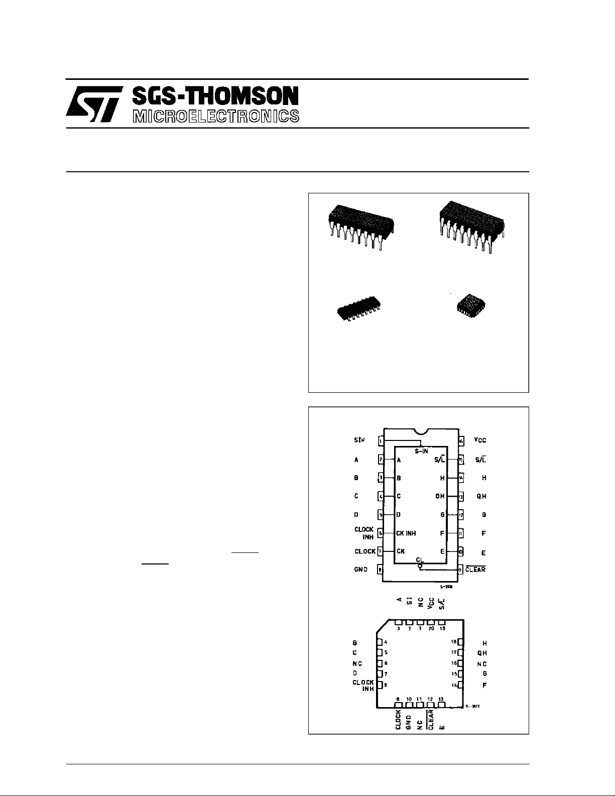
PIN CONNECTIONS(top view)
NC =
No InternalCon-
October 1992
1/13
Page 2
M54/M74HC166
INPUT AND OUTPUT EQUIVALENT CIRCUIT
PIN DESCRIPTION
IEC LOGIC SYMBOL
PIN No SYMBOL NAME AND FUNCTION
1 SI Serial Data Inputs
2, 3, 4, 5,
A to H Parallel Data Inputs
10, 11, 12,
14
6 CK INH Clock Enable Input
(Active LOW)
7 CK Clock Input (LOW to
HIGH edge-triggered)
9 CLEAR Asyncronous Master reset
Input (Active LOW)
13 Q
H
Serial Output from the
Last Stage
15 S/L ParallelEnable Input
(Active LOW)
8 GND Ground (0V)
16 V
CC
Positive Supply Voltage
TRUTH TABLE
INPUTS
CLEAR SHIFT/LOAD CLOCK INH CLOCK SERIAL IN
PARALLEL
...............
A
LXXXXXLLL
L X X X X NO CHANGE
HLL Xa
................
H H L H X H QAn QGn
H H L L X L QAn QGn
H X H X X X NO CHANGE
X:Don’tCare
...........
a
h : Thelevel ofsteady stateinput voltageat inputs a trough H respectively
INTERNAL
OUTPUTS
QA QB QH
H
OUTPUTS
ha b h
2/13
Page 3
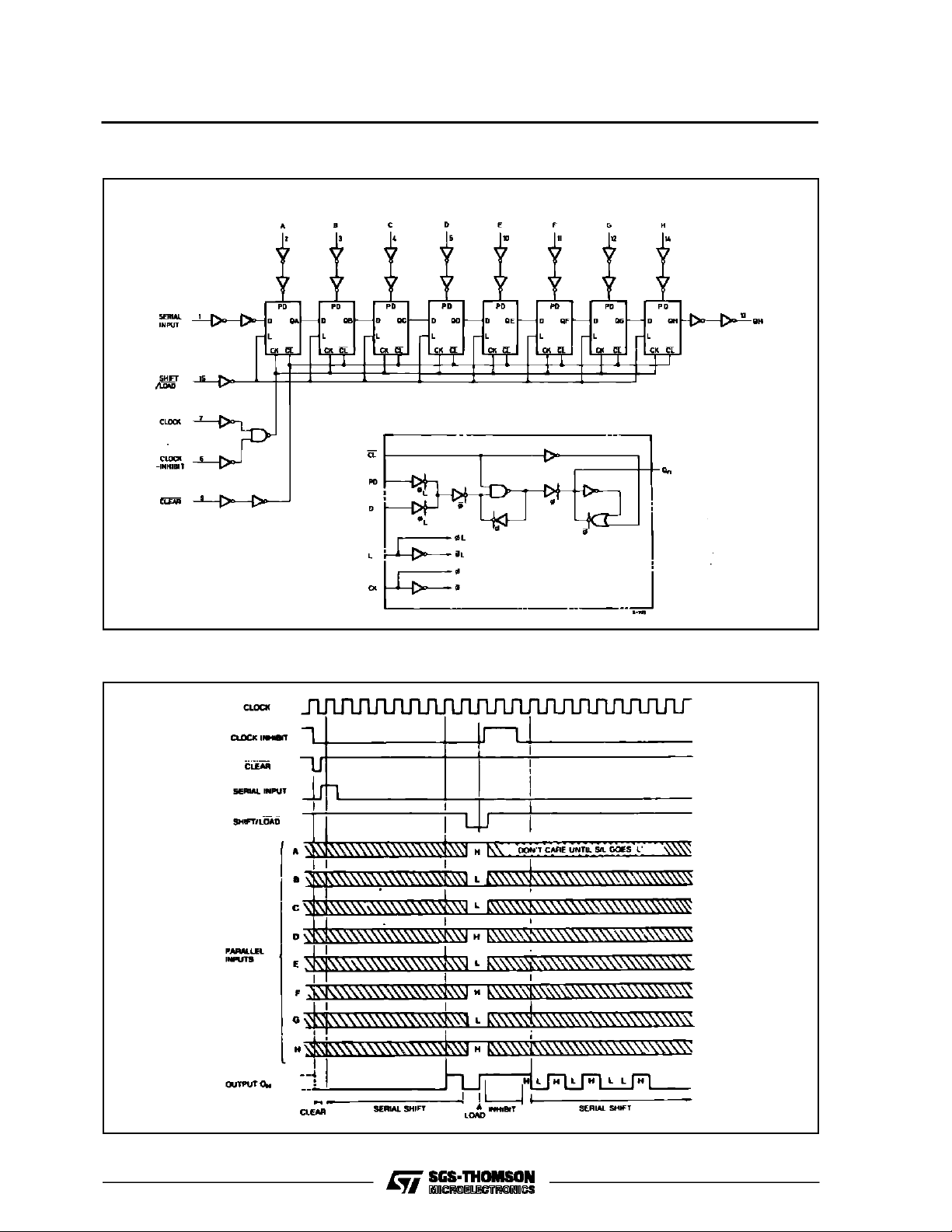
LOGIC DIAGRAM
M54/M74HC166
PARALLEL INPUTS
TIMING CHART
3/13
Page 4
M54/M74HC166
ABSOLU TE MAXIMU M RATINGS
Symbol Parameter Value Unit
V
CC
V
V
O
I
IK
I
OK
I
O
I
or I
CC
P
D
T
stg
T
AbsoluteMaximumRatingsarethose values beyondwhichdamage tothedevicemayoccur. Functionaloperationunder these conditionisnotimplied.
(*)500 mW: ≅ 65oC derateto300mWby 10mW/oC: 65oCto85oC
RECO MM ENDED O PERAT IN G C O NDITI O NS
Symbol Parameter Value Unit
V
CC
V
I
V
O
T
op
t
r,tf
Supply Voltage -0.5 to +7 V
DC Input Voltage -0.5 to VCC+ 0.5 V
I
DC Output Voltage -0.5 to VCC+ 0.5 V
DC Input Diode Current ± 20 mA
DC Output Diode Current ± 20 mA
DC Output Source Sink Current Per Output Pin ± 25 mA
DC VCCor Ground Current ± 50 mA
GND
Power Dissipation 500 (*) mW
Storage Temperature -65 to +150
Lead Temperature (10 sec) 300
L
Supply Voltage 2 to 6 V
Input Voltage 0 to V
Output Voltage 0 to V
Operating Temperature: M54HC Series
M74HC Series
CC
CC
-55 to +125
-40 to +85
Input Rise and Fall Time VCC= 2 V 0 to 1000 ns
V
= 4.5 V 0 to 500
CC
V
= 6 V 0 to 400
CC
o
C
o
C
V
V
o
C
o
C
4/13
Page 5

DC SPECIFICATIO NS
Symbol Parameter
V
V
V
V
I
High Level Input
IH
Voltage
Low Level Input
IL
Voltage
High Level
OH
Output Voltage
Low Level Output
OL
Voltage
I
Input Leakage
I
Current
Quiescent Supply
CC
Current
M54/M74HC166
Test Conditions Value
T
=25oC
V
(V)
CC
A
54HC and 74HC
Min. Typ. Max. Min. Max. Min. Max.
2.0 1.5 1.5 1.5
4.5 3.15 3.15 3.15
6.0 4.2 4.2 4.2
2.0 0.5 0.5 0.5
4.5 1.35 1.35 1.35
6.0 1.8 1.8 1.8
2.0
4.5 4.4 4.5 4.4 4.4
6.0 5.9 6.0 5.9 5.9
4.5 I
6.0 I
2.0
4.5 0.0 0.1 0.1 0.1
6.0 0.0 0.1 0.1 0.1
4.5 I
6.0 I
6.0
=
V
I
IO=-20 µA
V
IH
or
V
IL
=-4.0 mA 4.18 4.31 4.13 4.10
O
=-5.2 mA 5.68 5.8 5.63 5.60
O
V
=
I
IO=20µA
V
IH
or
V
IL
= 4.0 mA 0.17 0.26 0.33 0.40
O
= 5.2 mA 0.18 0.26 0.33 0.40
O
VI=VCCor GND ±0.1 ±1 ±1 µA
1.9 2.0 1.9 1.9
0.0 0.1 0.1 0.1
6.0 VI=VCCor GND 4 40 80 µA
-40 to 85oC
74HC
-55 to 125oC
54HC
Unit
V
V
V
V
5/13
Page 6

M54/M74HC166
AC ELECTRICAL CHARACTERISTICS (CL=50pF,Inputtr=tf=6ns)
Test Conditions Value
T
=25oC
Symbol Parameter
t
t
TLH
THL
Output Transition
Time
V
CC
(V)
2.0 30 75 95 110
4.5 8151922
A
54HC and 74HC
Min. Typ. Max. Min. Max. Min. Max.
6.0 7131619
t
PLH
t
PHL
t
PHL
f
MAX
Propagation
Delay Time
(CLOCK - QH)
Propagation
Delay Time
(CLEAR - QH)
Maximum Clock
Frequency
2.0 70 150 190 225
4.5 20 30 38 45
6.0 16 26 32 38
2.0 60 135 170 205
4.5 18 27 34 41
6.0 14 23 29 35
2.0 6.2 14 5.0 4.2
4.5 31 50 25 21
6.0 37 63 30 25
t
W(H)
t
W(L)
Minimum Pulse
Width
(CLOCK)
t
W(L)
Minimum Pulse
Width
(CLEAR)
Minimum Set-up
t
s
Time
(SI, PI)
Minimum Set-up
t
s
Time
(S/L)
Minimum Hold
t
h
Time
2.0 28 75 95 110
4.5 6151922
6.0 5131619
2.0 28 75 95 110
4.5 6151922
6.0 5131619
2.0 20 75 95 110
4.5 4151922
6.0 3131619
2.0 25 75 95 110
4.5 5151922
6.0 3131619
2.0 0 0 0
4.5 0 0 0
6.0 0 0 0
t
REM
Minimum
Removal Time
2.0 12 50 65 75
4.5 3101315
6.0 3 9 11 13
C
C
PD
Input Capacitance 5 10 10 10 pF
IN
(*) Power Dissipation
60
Capacitance
(*) CPDisdefined as the value ofthe IC’sinternal equivalent capacitance whichis calculated fromthe operatingcurrentconsumption without load.
(Referto Test Circuit). Average operting current canbe obtained bythefollowingequation. ICC(opr) = CPD•VCC•fIN+I
-40 to 85oC
74HC
-55 to 125oC
54HC
CC
Unit
ns
ns
ns
MHz
ns
ns
ns
ns
ns
ns
pF
6/13
Page 7

SWITCHING CHARACTERISTICS TEST WAVEFORM
CLEARMODE SERIAL MODE
PARALLEL MODE
M54/M74HC166
7/13
Page 8

M54/M74HC166
TEST CIRCUIT ICC(Opr.)
INPUT WAVEFORMIS THESAMEAS THAT IN CASEOF SWITCHINGCHARACTERISTICSTEST.
8/13
Page 9

Plastic DIP16 (0.25) MECHANICAL DATA
M54/M74HC166
DIM.
MIN. TYP. MAX. MIN. TYP. MAX.
a1 0.51 0.020
B 0.77 1.65 0.030 0.065
b 0.5 0.020
b1 0.25 0.010
D 20 0.787
E 8.5 0.335
e 2.54 0.100
e3 17.78 0.700
F 7.1 0.280
I 5.1 0.201
L 3.3 0.130
Z 1.27 0.050
mm inch
P001C
9/13
Page 10

M54/M74HC166
Ceramic DIP16/1 MECHANICAL DATA
DIM.
MIN. TYP. MAX. MIN. TYP. MAX.
A 20 0.787
B 7 0.276
D 3.3 0.130
E 0.38 0.015
e3 17.78 0.700
F 2.29 2.79 0.090 0.110
G 0.4 0.55 0.016 0.022
H 1.17 1.52 0.046 0.060
L 0.22 0.31 0.009 0.012
M 0.51 1.27 0.020 0.050
N 10.3 0.406
P 7.8 8.05 0.307 0.317
Q 5.08 0.200
mm inch
10/13
P053D
Page 11

SO16 (Narrow) MECHANICAL DATA
M54/M74HC166
DIM.
MIN. TYP. MAX. MIN. TYP. MAX.
A 1.75 0.068
a1 0.1 0.2 0.004 0.007
a2 1.65 0.064
b 0.35 0.46 0.013 0.018
b1 0.19 0.25 0.007 0.010
C 0.5 0.019
c1 45° (typ.)
D 9.8 10 0.385 0.393
E 5.8 6.2 0.228 0.244
e 1.27 0.050
e3 8.89 0.350
F 3.8 4.0 0.149 0.157
G 4.6 5.3 0.181 0.208
L 0.5 1.27 0.019 0.050
M 0.62 0.024
S8°(max.)
mm inch
P013H
11/13
Page 12

M54/M74HC166
PLCC20 MECHANICAL DATA
DIM.
MIN. TYP. MAX. MIN. TYP. MAX.
A 9.78 10.03 0.385 0.395
B 8.89 9.04 0.350 0.356
D 4.2 4.57 0.165 0.180
d1 2.54 0.100
d2 0.56 0.022
E 7.37 8.38 0.290 0.330
e 1.27 0.050
e3 5.08 0.200
F 0.38 0.015
G 0.101 0.004
M 1.27 0.050
M1 1.14 0.045
mm inch
12/13
P027A
Page 13

M54/M74HC166
Information furnishedis believed to be accurate and reliable. However, SGS-THOMSON Microelectronicsassumes no responsability for the
consequences of useof suchinformation nor forany infringement of patents or other rights of third parties which may results from its use. No
license is granted byimplication or otherwiseunder any patentor patentrights ofSGS-THOMSON Microelectronics.Specificationsmentioned
in this publication are subjectto changewithout notice. This publication supersedes andreplaces all information previously supplied.
SGS-THOMSON Microelectronicsproducts are not authorized foruse ascritical componentsinlife supportdevices orsystemswithoutexpress
written approval of SGS-THOMSON Microelectonics.
1994SGS-THOMSON Microelectronics- All Rights Reserved
Australia -Brazil - France - Germany - Hong Kong - Italy - Japan - Korea - Malaysia - Malta -Morocco - The Netherlands-
Singapore -Spain - Sweden- Switzerland - Taiwan - Thailand- UnitedKingdom - U.S.A
SGS-THOMSON Microelectronics GROUP OFCOMPANIES
13/13
 Loading...