

Page 1
SYNCHRONOUS PRESETTABLE 4-BIT COUNTER
■ HIGH SPEED :
f
= 62 MHz (TYP.) at VCC=6V
MAX
■ LOW POWER DISSIPATION:
ICC=4µA(MAX.) at TA=25°C
■ HIGH NOISE IMMUNITY:
V
NIH=VNIL
■ SYMMETRICAL OUTPUT IMPEDANCE:
|IOH|=IOL= 4mA (MIN)
■ BALANCED PROPAGATION DELAYS:
t
≅ t
PLH
■ WIDE OPERATING VOLTAGE RANGE:
VCC(OPR) = 2V to 6V
■ PIN AND FUNCTION COMPATIBLE WITH
74 SERIES 161
DESCRIPTION
The M74HC161 is an high speed CMOS
SYNCHRONOUS 4-BIT BINARY
PRESETTABLE COUNTERfabricatedwith silicon
gate C2MOS technology.
The CLOCK input is active on the rising edge.
Both LOAD and CLEAR inputs are active LOW.
Presetting is synchronous on the rising edge of
the clock, the function is cleared asynchronously.
=28%VCC(MIN.)
PHL
M74HC161
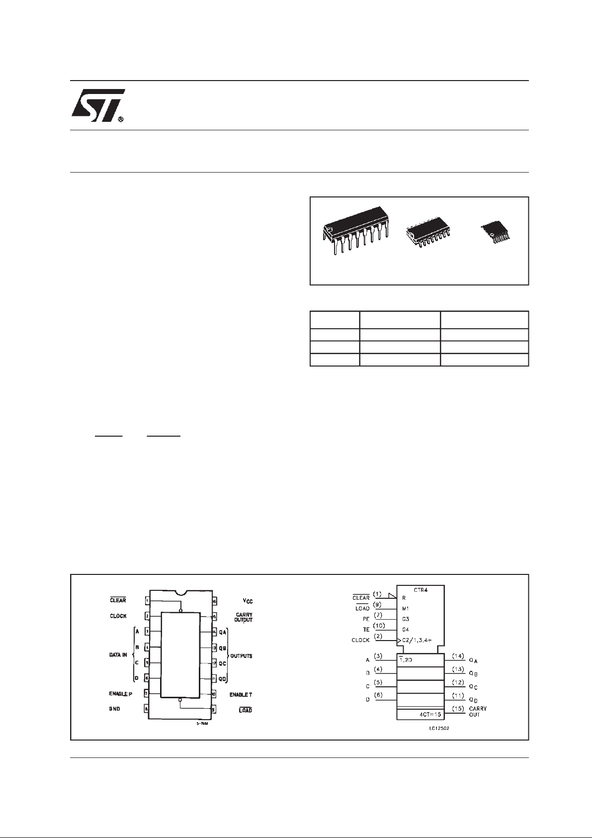
TSSOPDIP SOP
ORDER CODES
PACKAGE TUBE T & R
DIP M74HC161B1R
SOP M74HC161M1R M74HC161RM13TR
TSSOP M74HC161TTR
Two enable inputs (TE and PE) and CARRY
output are provided to enable easy cascading of
counters, which facilities easy implementation of
N-bit counters without using external gates.
All inputs are equipped with protection circuits
against static discharge and transient excess
voltage.
PIN CONNECTION AND IEC LOGIC SYMBOLS
1/12July 2001
Page 2
M74HC161
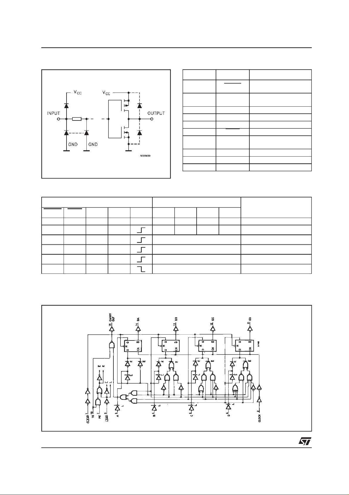
INPUT AND OUTPUT EQUIVALENT CIRCUIT PIN DESCRIPTION
PIN No SYMBOL NAME AND FUNCTION
1 CLEAR
2 CLOCK
3, 4, 5, 6 A, B, C, D Data Inputs
7 PE Count Enable Input
10 TE Count Enable Carry Input
9 LOAD Parallel Enable Input
14, 13, 12,
11
15 CARRY Terminal Count Output
8 GND Ground (0V)
16 Vcc Positive Supply Voltage
TRUTH TABLE
QA to QD Flip Flop Outputs
Asynchronous Master
Reset
Clock Input (LOW to
HIGH, Edge-triggered)
INPUTS OUTPUTS
FUNCTION
CLEAR LOAD PE TE CLOCK QA QB QC QD
LXXXXLLLL RESET TO ”0”
H L X X A B C D PRESET DATA
H H X L NO CHANGE NO COUNT
H H L X NO CHANGE NO COUNT
HHHH COUNT UP COUNT
H X X X NOCHANGE NO COUNT
X : Don’t Care
A, B, C, D : Logic level of data inputs
Carry : CARRY =TE·Q
A·QB·QC·QD
LOGIC DIAGRAM
This logic diagram has not be used to estimate propagation delays
2/12
Page 3

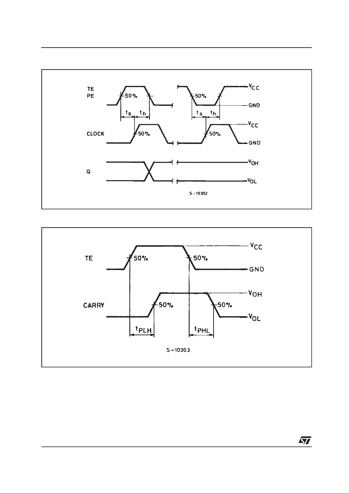
TIMING CHART
M74HC161
ABSOLUTE MAXIMUM RATINGS
Symbol Parameter Value Unit
V
V
V
I
I
OK
I
or I
I
CC
P
T
T
Absolute Maximum Ratings are those values beyond which damage to thedevice may occur. Functional operation under these conditions is
not implied
(*) 500mW at 65
Supply Voltage
CC
DC Input Voltage -0.5 to VCC+ 0.5
I
DC Output Voltage -0.5 to VCC+ 0.5
O
DC Input Diode Current
IK
DC Output Diode Current
DC Output Current
O
DC VCCor Ground Current
GND
Power Dissipation
D
Storage Temperature
stg
Lead Temperature (10 sec)
L
°C; derate to 300mW by 10mW/°C from 65°Cto85°C
-0.5 to +7 V
V
V
± 20 mA
± 20 mA
± 25 mA
± 50 mA
500(*) mW
-65 to +150 °C
300 °C
3/12
Page 4

M74HC161
RECOMMENDED OPERATING CONDITIONS
Symbol Parameter Value Unit
V
V
V
T
t
r,tf
DC SPECIFICATIONS
Symbol Parameter
V
IH
V
IL
V
OH
V
OL
I
I
I
CC
Supply Voltage
CC
Input Voltage 0 to V
I
Output Voltage 0 to V
O
Operating Temperature
op
Input Rise and Fall Time VCC= 2.0V
= 4.5V
V
CC
= 6.0V
V
CC
Test Condition Value
=25°C
T
A
Min. Typ. Max. Min. Max. Min. Max.
High Level Input
V
CC
(V)
2.0 1.5 1.5 1.5
Voltage
6.0 4.2 4.2 4.2
Low Level Input
2.0 0.5 0.5 0.5
Voltage
6.0 1.8 1.8 1.8
High Level Output
Voltage
Low Level Output
Voltage
Input Leakage
Current
Quiescent Supply
Current
2.0
4.5
6.0
4.5
6.0
2.0
4.5
6.0
4.5
6.0
6.0
6.0
I
I
I
I
O
I
O
I
I
V
I=VCC
V
I=VCC
=-20 µA
O
=-20 µA
O
=-20 µA
O
=-4.0 mA
=-5.2 mA
I
=20 µA
O
=20 µA
I
O
I
=20 µA
O
=4.0 mA
O
=5.2 mA
O
or GND
or GND
1.9 2.0 1.9 1.9
4.4 4.5 4.4 4.4
5.9 6.0 5.9 5.9
4.18 4.31 4.13 4.10
5.68 5.8 5.63 5.60
0.0 0.1 0.1 0.1
0.0 0.1 0.1 0.1
0.0 0.1 0.1 0.1
0.17 0.26 0.33 0.40
0.18 0.26 0.33 0.40
± 0.1 ± 1 ± 1 µA
44080µA
2to6 V
CC
CC
-55 to 125 °C
0 to 1000 ns
0 to 500 ns
0 to 400 ns
-40 to 85°C -55 to 125°C
V
V
Unit
V4.5 3.15 3.15 3.15
V4.5 1.35 1.35 1.35
V
V
4/12
Page 5
AC ELECTRICAL CHARACTERISTICS (CL= 50 pF, Input tr=tf= 6ns)
Test Condition Value
=25°C
Symbol Parameter
t
TLHtTHL
t
PLHtPHL
Output Transition
Time
Propagation Delay
Time
(CLOCK - Q)
t
PLHtPHL
Propagation Delay
Time
(CLOCK - CARRY)
t
PLHtPHL
Propagation Delay
Time
(TE - CARRY)
t
Propagation Delay
PLH
Time
(CLEAR - Q)
t
Propagation Delay
PHL
Time
(CLEAR - CARRY)
f
MAX
t
W(H)
t
W(L)
t
W(L)
Maximum Clock
Frequency
Minimum Pulse
Width (CLOCK)
Minimum Pulse
Width (CLEAR)
t
Minimum Set-up
s
Time
(LOAD, PE, TE)
t
Minimum Set-up
s
Time
(A, B, C, D)
t
Minimum Hold
h
Time
(A, B - CLOCK)
t
REM
Minimum Removal
Time
V
CC
(V)
2.0 25 75 95 110
6.0 6131619
2.0 48 125 155 190
6.0 14 21 26 32
2.0 57 150 190 225
6.0 16 26 32 38
2.0 39 100 125 150
6.0 11 17 21 26
2.0 60 150 190 225
6.0 17 26 32 38
2.0 72 200 250 300
6.0 20 34 43 51
2.0 6.2 18 5 4.2
6.0 37 62 30 25
2.0 18 75 95 110
6.0 6131619
2.0 24 75 95 110
6.0 6131619
2.0 40 100 125 150
6.0 8172126
2.0 20 75 95 110
6.0 3131619
2.0 0 0 0
6.0 0 0 0
2.0 18 50 65 75
6.0 3 9 11 13
T
A
Min. Typ. Max. Min. Max. Min. Max.
M74HC161
-40 to 85°C -55 to 125°C
Unit
ns4.5 7151922
ns4.5 16 25 31 38
ns4.5 19 30 38 45
ns4.5 13 20 25 30
ns4.5 20 30 38 45
ns4.5 24 40 50 60
MHz4.5 31 53 25 21
ns4.5 6151922
ns4.5 7151922
ns4.5 10 20 25 30
ns4.5 5151922
ns4.5 0 0 0
ns4.5 4101315
5/12
Page 6

M74HC161
CAPACITIVE CHARACTERISTICS
Test Condition Value
=25°C
Symbol Parameter
C
C
1) CPDis defined as the value of the IC’s internal equivalent capacitance whichis calculated from the operating current consumption without
load. (Refer to Test Circuit). Average operating current can be obtained by the following equation. I
Input Capacitance
IN
Power Dissipation
PD
Capacitance (note1)5.0 50 pF
V
CC
(V)
5.0 5101010pF
TEST CIRCUIT
T
A
-40 to 85°C -55 to 125°C
Min. Typ. Max. Min. Max. Min. Max.
CC(opr)=CPDxVCCxfIN+ICC
Unit
CL= 50pF or equivalent (includes jig and probe capacitance)
R
T=ZOUT
of pulse generator (typically 50Ω)
WAVEFORM 1: PROPAGATION DELAY TIMES, CLOCK MINIMUM PULSE WIDTH
(f=1MHz; 50% duty cycle)
6/12
Page 7

M74HC161
WAVEFORM 2 : PROPAGATION DELAY TIMES,CLEAR MINIMUM PULSE WIDTH (CLEAR MODE)
(f=1MHz; 50% duty cycle)
WAVEFORM 3 : SETUP AND HOLD TIMES (PRESET MODE) (f=1MHz; 50% duty cycle)
7/12
Page 8
M74HC161
WAVEFORM 4 : SETUP AND HOLD TIMES (COUNTENABLE MODE) (f=1MHz; 50% duty cycle)
WAVEFORM 5 :PROPAGATION DELAY TIMES(CASCADE MODE) (f=1MHz;50% dutycycle)
8/12
Page 9

M74HC161
Plastic DIP-16 (0.25) MECHANICAL DATA
mm. inch
DIM.
MIN. TYP MAX. MIN. TYP. MAX.
a1 0.51 0.020
B 0.77 1.65 0.030 0.065
b 0.5 0.020
b1 0.25 0.010
D 20 0.787
E 8.5 0.335
e 2.54 0.100
e3 17.78 0.700
F 7.1 0.280
I 5.1 0.201
L 3.3 0.130
Z 1.27 0.050
P001C
9/12
Page 10

M74HC161
SO-16 MECHANICAL DATA
DIM.
A 1.75 0.068
a1 0.1 0.2 0.003 0.007
a2 1.65 0.064
b 0.35 0.46 0.013 0.018
b1 0.19 0.25 0.007 0.010
C 0.5 0.019
c1 45° (typ.)
D 9.8 10 0.385 0.393
E 5.8 6.2 0.228 0.244
e 1.27 0.050
e3 8.89 0.350
F 3.8 4.0 0.149 0.157
G 4.6 5.3 0.181 0.208
L 0.5 1.27 0.019 0.050
M 0.62 0.024
S8°(max.)
MIN. TYP MAX. MIN. TYP. MAX.
mm. inch
10/12
PO13H
Page 11

M74HC161
TSSOP16 MECHANICAL DATA
mm. inch
DIM.
MIN. TYP MAX. MIN. TYP. MAX.
A 1.2 0.047
A1 0.05 0.15 0.002 0.004 0.006
A2 0.8 1 1.05 0.031 0.039 0.041
b 0.19 0.30 0.007 0.012
c 0.09 0.20 0.004 0.0089
D 4.9 5 5.1 0.193 0.197 0.201
E 6.2 6.4 6.6 0.244 0.252 0.260
E1 4.3 4.4 4.48 0.169 0.173 0.176
e 0.65 BSC 0.0256 BSC
K0° 8°0° 8°
L 0.45 0.60 0.75 0.018 0.024 0.030
A2
A
A1
b
e
c
K
L
E
D
E1
PIN 1 IDENTIFICATION
1
0080338D
11/12
Page 12

M74HC161
Information furnished is believed to be accurate and reliable. However, STMicroelectronics assumes no responsibility for the
consequences of use of such information nor for any infringement of patents or other rights ofthird parties which may resultfrom
its use. No license is granted by implication or otherwise under any patent or patent rights of STMicroelectronics. Specifications
mentioned in this publication are subject to change without notice. This publication supersedes and replaces all information
previously supplied. STMicroelectronics prod ucts are not authorized for use as critical components in life support devices or
systems without express written approval of STMicroelectronics.
Australia - Brazil - China - Finland - France - Germany - Hong Kong - India - Italy - Japan - Malaysia - Malta - Morocco
The ST logo is a registered trademark of STMicroelectronics
2001 STMicroelectronics - Printed in Italy - All Rights Reserved
STMicroelectronics GROUP OF COMPANIES
Singapore - Spain - Sweden - Switzerland - United Kingdom
http://w ww.st.com
12/12
 Loading...