

Page 1
HC157 QUAD 2 CHANNEL MULTIPLEXER
HC158 QUAD 2 CHANNEL MULTIPLEXER(INV.)
.HIGH SPEED
tPD= 10 ns (TYP.) AT VCC=5V
.LOWPOWER DISSIPATION
ICC=4 µA (MAX.) AT TA=25 °C
.HIGH NOISE IMMUNITY
V
NIH=VNIL
=28%VCC(MIN.)
.OUTPUTDRIVE CAPABILITY
10 LSTTL LOADS
.SYMMETRICALOUTPUT IMPEDANCE
IOH =IOL= 4 mA(MIN.)
.BALANCEDPROPAGATIONDELAYS
t
PLH=tPHL
.WIDE OPERATINGVOLTAGE RANGE
VCC(OPR)= 2 V TO 6 V
.PIN ANDFUNCTION COMPATIBLE
WITH 54/74LS157/158
M54HC157/158
M7 4HC1 57 /1 58
B1R
(PlasticPackage)
M1R
(MicroPackage)
ORDER CODES :
M54HC X XXF1R M74H CXXXM1R
M74HC X XXB1R M74HCX X XC1R
F1R
(CeramicPackage)
C1R
(Chip Carrier)
DESCRIPTION
The M54/74HC157 and theM54/74HC158arehigh
speed CMOS QUAD 2-CHANNEL MULTIPLEXER’sfabricated withsilicongate C2MOStechnology. They achieve the high speed operation
similar to equivalent LSTTL while maintaining the
CMOS low powerdissipation.
These devices consist of four 2-input digital multiplexerswithcommon select and strobe inputs. The
HC158 is an inverting multiplexer while the HC157
is a non-inverting multiplexer. When the STROBE
inputis held High, selection of data is inhibited and
all the outputs become Low in the M74HC157 and
High in the M74HC158. The SELECT decoding
determines whether the A or B inputs get routed to
their corresponding Y outputs. All inputs are
equipped with protection circuits against static discharge and transient excess voltage.
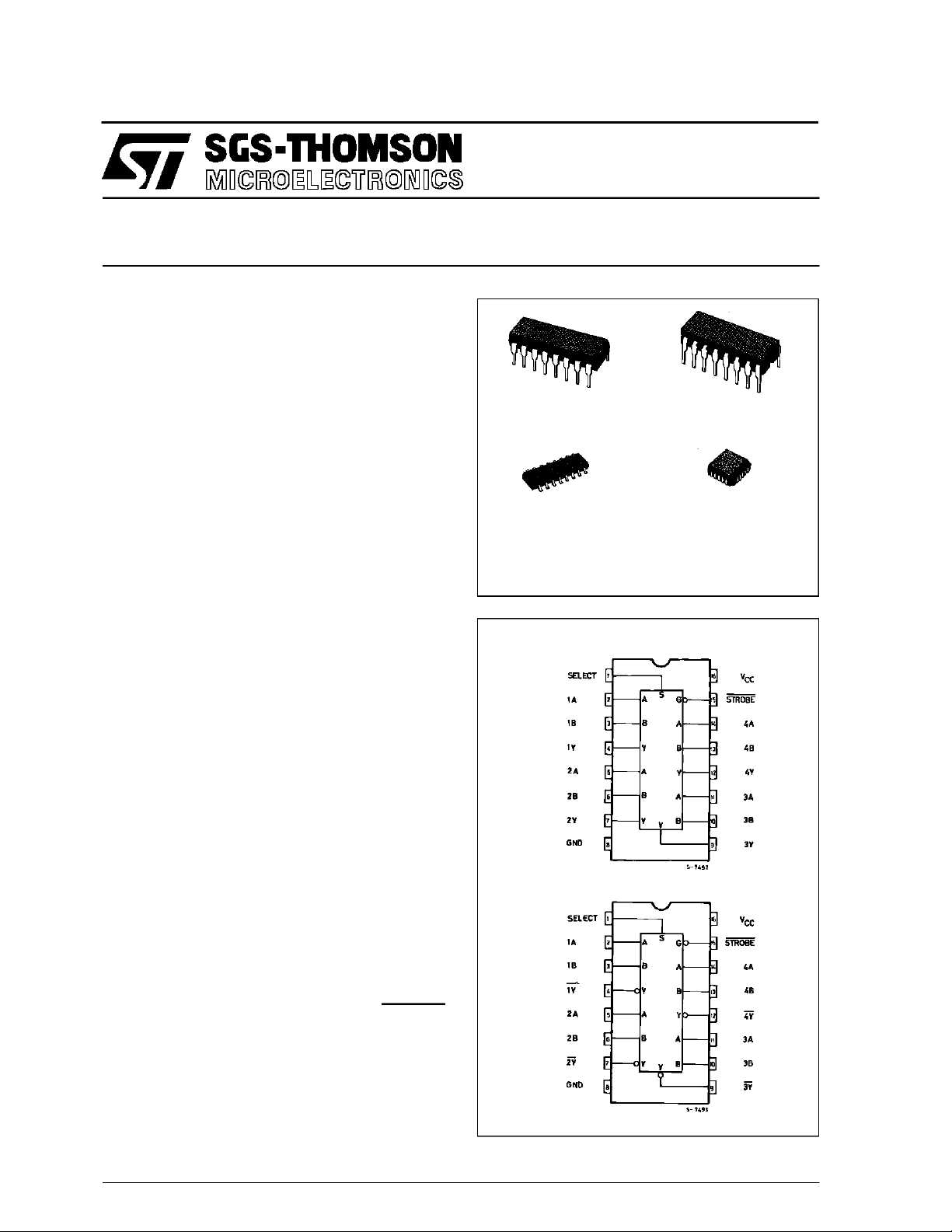
PIN CONNECTIONS(top view)
HC157
HC158
NC =
No Internal
Connection
February 1993
1/11
Page 2
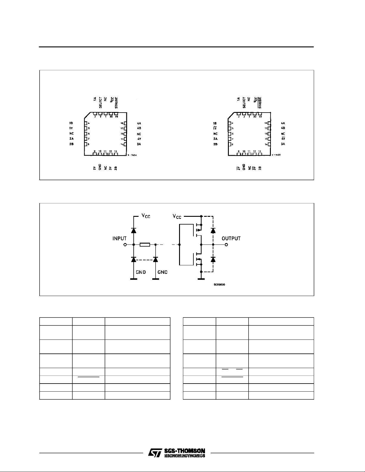
M54/M74HC157 M54/M74HC158
CHIP CARRIER
HC157 HC158
INPUT AND OUTPUT EQUIVALENT CIRCUIT
PIN DESCRIPTION ( f or HC157)
PIN No SYMBOL NAME AND FUNCTION
1 SELECT Common Data Select
Input
2, 5, 11, 14 1A to 4A Data Inputs From
Source A
3, 6, 10, 13 1B to 4B Data Inputs From
Source B
4, 7, 9, 12 1Y to 4Y Multiplexer Output
15 STROBE Strobe Input
8 GND Ground (0V)
16 V
2/11
CC
Positive Supply Voltage
PIN DESCRIPTION (for HC158)
PIN No SYMBOL NAME AND FUNCTION
1 SELECT Common Data Select
Input
2, 5, 11, 14 1A to 4A Data Inputs From
Source A
3, 6, 10, 13 1B to 4B Data Inputs From
Source B
4, 7, 9, 12 1Y to 4Y Multiplexer Output
15 STROBE Strobe Input
8 GND Ground (0V)
16 V
CC
Positive Supply Voltage
Page 3
M54/M74HC157 M 54/M74 HC158
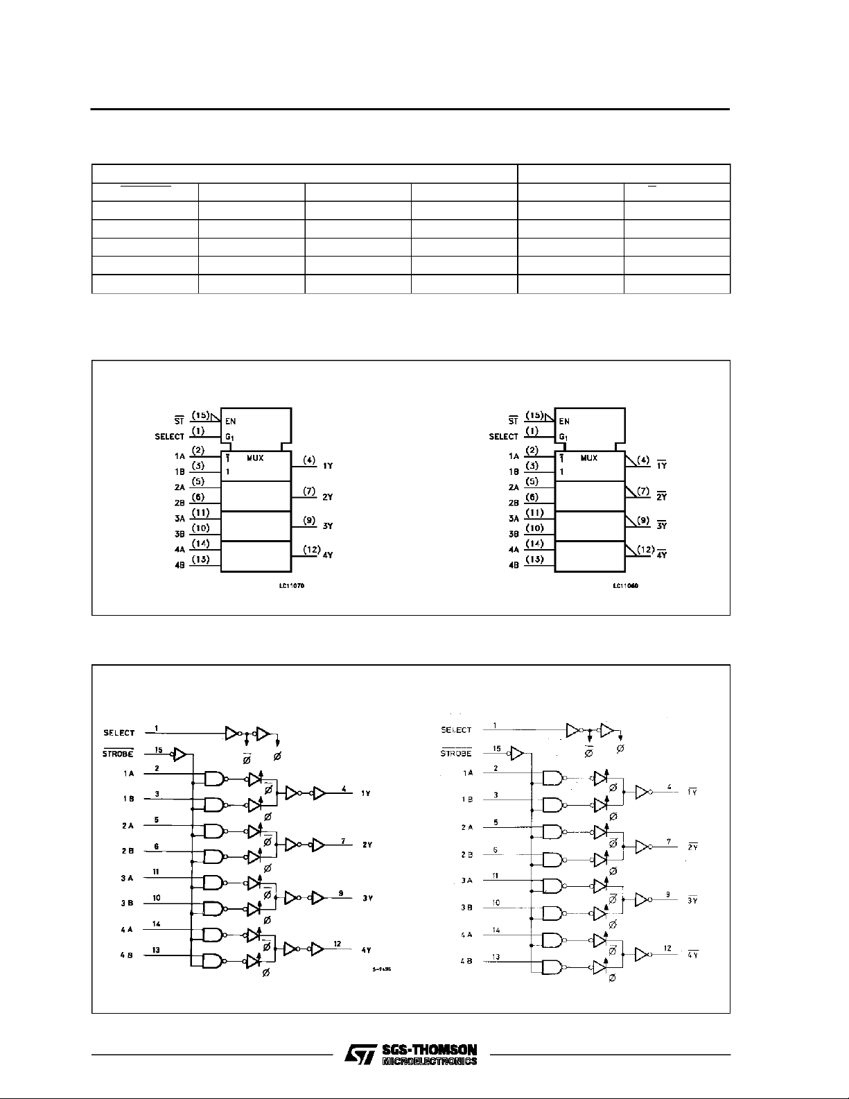
TRUTH TABLE
INPUTS OUTPUTS
STROBE SELECT A B Y (HC157) Y (HC158)
HXXXLH
LLLXLH
LLHXHL
LHXLLH
LHXHHL
X:DON’TCARE
IEC LOGIC SYMBOL
HC157 HC158
LOGIC DIAGRAM
HC157 HC158
3/11
Page 4
M54/M74HC157 M54/M74HC158
ABSOLU TE M AXIMU M R AT INGS
Symbol Parameter Value Unit
V
CC
V
V
O
I
IK
I
OK
I
O
I
or I
CC
P
D
T
stg
T
L
AbsoluteMaximumRatingsare thosevaluesbeyond whichdamage tothedevicemayoccur.Functional operationunder theseconditionisnotimplied.
(*)500 mW:≅65oC derate to300 mW by 10mW/oC: 65oCto85oC
RECO MM ENDED OPERAT I N G C ONDITIONS
Symbol Parameter Value Unit
V
CC
V
I
V
O
T
op
t
r,tf
Supply Voltage -0.5 to +7 V
DC Input Voltage -0.5 to VCC+ 0.5 V
I
DC Output Voltage -0.5 to VCC+ 0.5 V
DC Input Diode Current ± 20 mA
DC Output Diode Current ± 20 mA
DC Output Source Sink Current Per Output Pin ± 25 mA
DC VCCor Ground Current ± 50 mA
GND
Power Dissipation 500 (*) mW
Storage Temperature -65 to +150
Lead Temperature (10 sec) 300
Supply Voltage 2 to 6 V
Input Voltage 0 to V
Output Voltage 0 to V
Operating Temperature: M54HC Series
M74HC Series
CC
CC
-55 to +125
-40 to +85
Input Rise and Fall Time VCC= 2 V 0 to 1000 ns
V
= 4.5 V 0 to 500
CC
V
= 6 V 0 to 400
CC
o
C
o
C
V
V
o
C
o
C
4/11
Page 5

DC SPECIFICATIONS
Symbol Parameter
V
V
V
V
I
I
* Applicable only toDIR, G, G input
High Level Input
IH
Voltage
Low Level Input
IL
Voltage
High Level
OH
Output Voltage
Low Level Output
OL
Voltage
* Input Leakage
I
Current
Quiescent Supply
CC
Current
M54/M74HC157 M 54/M74 HC158
Test Conditions Value
T
=25oC
V
(V)
CC
A
54HC and 74HC
Min. Typ. Max. Min. Max. Min. Max.
2.0 1.5 1.5 1.5
4.5 3.15 3.15 3.15
6.0 4.2 4.2 4.2
2.0 0.5 0.5 0.5
4.5 1.35 1.35 1.35
6.0 1.8 1.8 1.8
2.0
4.5 4.4 4.5 4.4 4.4
6.0 5.9 6.0 5.9 5.9
4.5 I
6.0 I
2.0
4.5 0.0 0.1 0.1 0.1
6.0 0.0 0.1 0.1 0.1
4.5 I
6.0 I
6.0
=
V
I
IO=-20 µA
V
IH
or
V
IL
=-4.0 mA 4.18 4.31 4.13 4.10
O
=-5.2 mA 5.68 5.8 5.63 5.60
O
V
=
I
IO=20µA
V
IH
or
V
IL
= 4.0 mA 0.17 0.26 0.33 0.40
O
= 5.2 mA 0.18 0.26 0.33 0.40
O
VI=VCCor GND ±0.1 ±1 ±1 µA
1.9 2.0 1.9 1.9
0.0 0.1 0.1 0.1
6.0 VI=VCCor GND
I
=0
O
-40 to 85oC
74HC
-55 to 125oC
54HC
44080µA
Unit
V
V
V
V
5/11
Page 6

M54/M74HC157 M54/M74HC158
AC ELECTRICAL CHARACTERISTICS (CL=50pF,Inputtr=tf=6ns)
Test Conditions Value
T
=25oC
Symbol Parameter
t
t
TLH
THL
Output Transition
Time
V
CC
(V)
2.0 30 75 95 110
4.5 8151922
A
54HC and 74HC
Min. Typ. Max. Min. Max. Min. Max.
6.0 7131619
t
PLH
t
PHL
Propagation
Delay Time
(A, B - Y)
t
t
PLH
PHL
Propagation
Delay Time
(SELECT - Y)
t
t
PLH
PHL
Propagation
Delay Time
(STROBE - Y)
C
C
PD
Input Capacitance 5 10 10 10 pF
IN
(*) Power Dissipation
2.0 30 100 125 150
4.5 12 20 25 30
6.0 10 17 21 26
2.0 50 125 155 190
4.5 16 25 31 38
6.0 14 21 26 32
2.0 36 115 145 175
4.5 12 23 29 35
6.0 10 20 25 30
47
Capacitance
(*) CPDisdefined asthe valueofthe IC’s internal equivalent capacitance which is calculated from the operating currentconsumption without load.
(RefertoTestCircuit).Average opertingcurrentcanbe obtained bythefollowingequation. ICC(opr) = CPD•VCC•fIN+ICC/4(per channel)
-40 to 85oC
74HC
-55 to 125oC
54HC
Unit
ns
ns
ns
ns
pF
SWITCHING CHARACTERISTICS TEST CIRCUIT
TEST CIRCUIT ICC(Opr.)
INPUTWAVEFORMIS THE SAME AS THATIN CASEOF
SWITCHINGCHARACTERISTICSTEST.
6/11
Page 7

M54/M74HC157 M 54/M74 HC158
Plastic DIP16 (0.25) MECHANICAL DATA
DIM.
MIN. TYP. MAX. MIN. TYP. MAX.
a1 0.51 0.020
B 0.77 1.65 0.030 0.065
b 0.5 0.020
b1 0.25 0.010
D 20 0.787
E 8.5 0.335
e 2.54 0.100
e3 17.78 0.700
F 7.1 0.280
I 5.1 0.201
L 3.3 0.130
Z 1.27 0.050
mm inch
P001C
7/11
Page 8

M54/M74HC157 M54/M74HC158
Ceramic DIP16/1 MECHANICAL DATA
DIM.
MIN. TYP. MAX. MIN. TYP. MAX.
A 20 0.787
B 7 0.276
D 3.3 0.130
E 0.38 0.015
e3 17.78 0.700
F 2.29 2.79 0.090 0.110
G 0.4 0.55 0.016 0.022
H 1.17 1.52 0.046 0.060
L 0.22 0.31 0.009 0.012
M 0.51 1.27 0.020 0.050
N 10.3 0.406
P 7.8 8.05 0.307 0.317
Q 5.08 0.200
mm inch
8/11
P053D
Page 9

M54/M74HC157 M 54/M74 HC158
SO16 (Narrow) MECHANICAL DATA
DIM.
MIN. TYP. MAX. MIN. TYP. MAX.
A 1.75 0.068
a1 0.1 0.2 0.004 0.007
a2 1.65 0.064
b 0.35 0.46 0.013 0.018
b1 0.19 0.25 0.007 0.010
C 0.5 0.019
c1 45° (typ.)
D 9.8 10 0.385 0.393
E 5.8 6.2 0.228 0.244
e 1.27 0.050
e3 8.89 0.350
F 3.8 4.0 0.149 0.157
G 4.6 5.3 0.181 0.208
L 0.5 1.27 0.019 0.050
M 0.62 0.024
S8°(max.)
mm inch
P013H
9/11
Page 10

M54/M74HC157 M54/M74HC158
PLCC20 MECHANICAL DATA
DIM.
MIN. TYP. MAX. MIN. TYP. MAX.
A 9.78 10.03 0.385 0.395
B 8.89 9.04 0.350 0.356
D 4.2 4.57 0.165 0.180
d1 2.54 0.100
d2 0.56 0.022
E 7.37 8.38 0.290 0.330
e 1.27 0.050
e3 5.08 0.200
F 0.38 0.015
G 0.101 0.004
M 1.27 0.050
M1 1.14 0.045
mm inch
10/11
P027A
Page 11

M54/M74HC157 M 54/M74 HC158
Information furnished is believed to be accurate and reliable. However, SGS-THOMSON Microelectronics assumes no responsability for the
consequences of use of such information nor forany infringement of patents orother rights of third parties which may results from its use. No
license isgranted by implication orotherwise under any patentor patentrights ofSGS-THOMSON Microelectronics. Specificationsmentioned
in this publication are subject to changewithout notice. This publication supersedes and replaces all information previously supplied.
SGS-THOMSON Microelectronicsproductsare notauthorizedforuse ascriticalcomponentsinlife supportdevices or systemswithoutexpress
written approvalof SGS-THOMSON Microelectonics.
1994 SGS-THOMSON Microelectronics- All RightsReserved
Australia - Brazil - France - Germany - Hong Kong - Italy - Japan - Korea - Malaysia - Malta - Morocco - The Netherlands -
Singapore - Spain - Sweden- Switzerland - Taiwan - Thailand - United Kingdom - U.S.A
SGS-THOMSON Microelectronics GROUP OF COMPANIES
11/11
 Loading...