

Page 1
M54HC153/253
M74HC153/253
HC153 DUAL 4 CHANNEL MULTIPLEXER
HC253 DUAL 4 CHANNEL MULTIPLEXER 3 STATE OUTPUT
.HIGH SPEED
tPD= 12 ns(TYP.) at VCC=5V
.LOWPOWERDISSIPATION
ICC=4µA(MAX.) at TA=25°C
.HIGH NOISEIMMUNITY
V
NIH=VNIL
.OUTPUT DRIVE CAPABILITY
10 LSTTL LOADS
=28%VCC(MIN.)
B1R
(PlasticPackage)
F1R
(CeramicPackage)
.SYMMETRICALOUTPUT IMPEDANCE
IOH=IOL=4 mA(MIN.)
.BALANCEDPROPAGATION DELAYS
t
PLH=tPHL
.WIDE OPERATINGVOLTAGE RANGE
VCC(OPR)= 2V to6V
.PIN AND FUNCTION COMPATIBLE WITH
54/74LS153/253
M1R
(MicroPackage)
ORDER CODES :
M54HC X XXF1R M74H CXXXM1R
M74HC X XXB1R M74HCX X XC1R
C1R
(Chip Carrier)
DESCRIPTION
The M54/74HC153 and M54/74HC253 are high
speedCMOSDUAL4-CHANNEL MULTIPLEXERS
fabricated with silicon gate C2MOS technology.
Bothachieve highspeed operation, similar to equivalent LSTTL, while maintaining the CMOS low
powerdissipation.
The designer has a choiceof complementary output
(HC153) and3-stateoutput (HC253).
Eachofthesedata(1C0-1C3, 2C0-2C3) isselected
by the two address inputs A and B.
Separate strobe inputs (1G, 2G) are provided for
eachof the two four-line sections. The strobeinput
(G)canbe usedto inhibit thedataoutput ;theoutput
of HC 153 is fixed at a low level and the output of
HC253 is a high impedance, while the strobeinput
is heldlow.
All inputs are equipped with protection circuits
against static discharge and transient excess voltage.
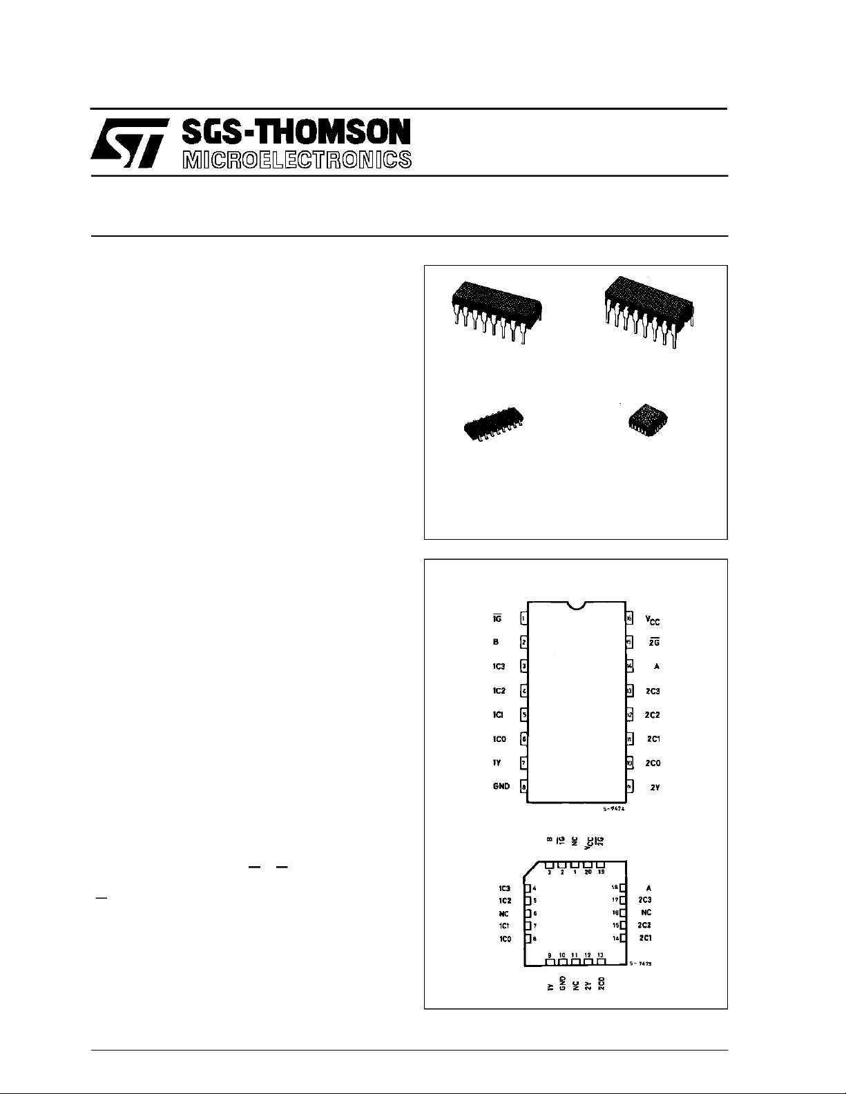
PIN CONNECTIONS(top view)
NC =
No Internal
Connection
January 1993
1/12
Page 2
M54/M74HC153 M54/M74HC253
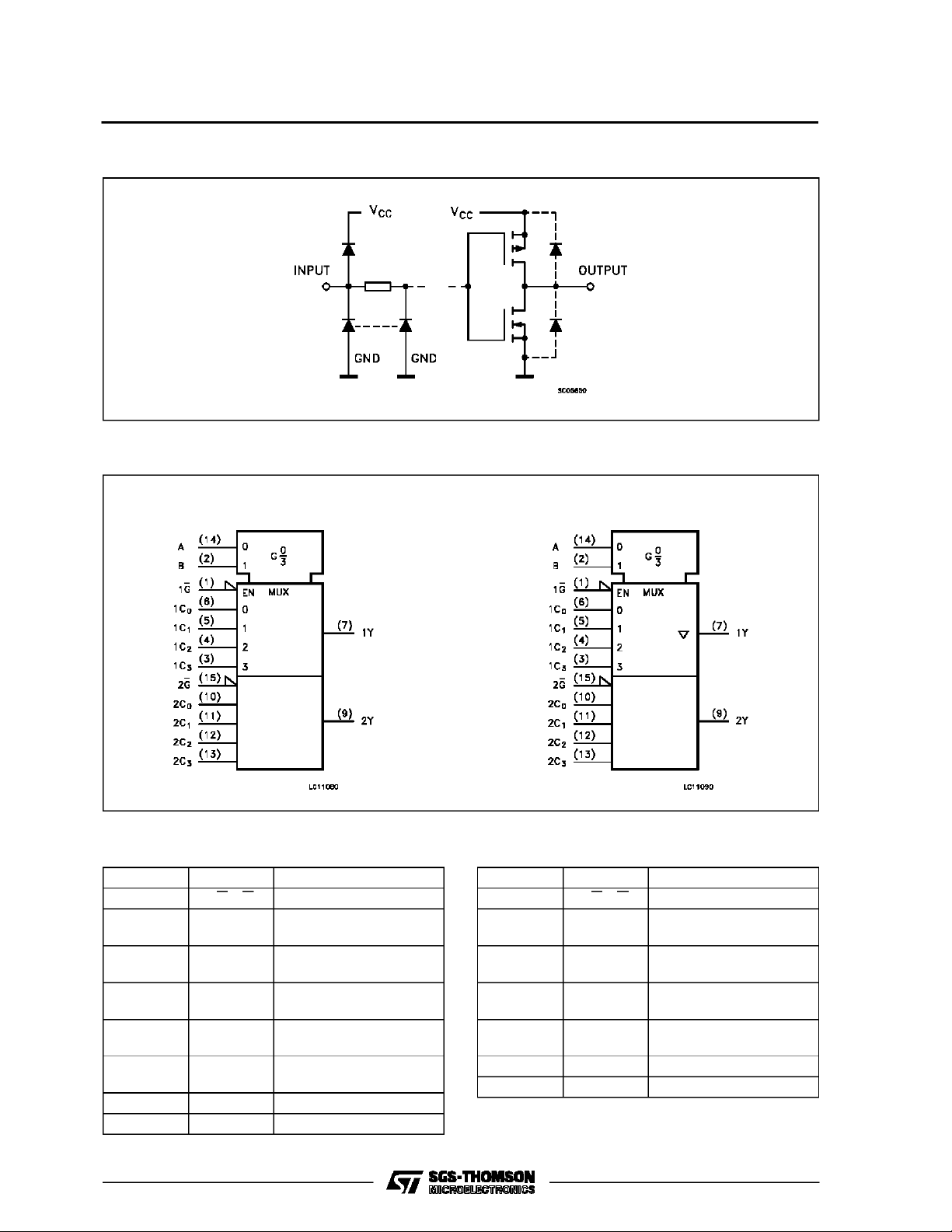
INPUT AND OUTPUT EQUIVALENT CIRCUIT
IEC LOGIC SYMBOLS
HC153 HC253
PIN DESC RIPTION (for HC153)
PIN No SYMBOL NAME AND FUNCTION
1, 15 1G, 2G Output Enable Inputs
14, 2 A, B Common Data Select
Inputs
6, 5, 4, 3 1C0 to 1C3 Data Inputs From
Source 1
7 1Y Multiplexer Output From
Source 1
9 2Y Multiplexer Output From
Source 2
10, 11, 12,132C0 to 2C3 Data Inputs From
Source 2
8 GND Ground (0V)
16 V
2/12
CC
Positive Supply Voltage
PIN DESCRIPTIO N (for H C253)
PIN No SYMBOL NAME AND FUNCTION
1, 15 1G, 2G Output Enable Inputs
14, 2 A, B Common Data Select
Inputs
6, 5, 4, 3 1C0 to 1C3 Data Inputs From
Source 1
7, 9 1Y, 2Y 3 State Multiplexer
Outputs
10, 11, 12,132C0 to 2C3 Data Inputs From
Source 2
8 GND Ground (0V)
16 V
CC
Positive Supply Voltage
Page 3
M54/M 74HC1 53 M54/M7 4 HC 253
TRUTH TABLE
SELECT INPUTS DATA INPUTS STROBE OUTPUT Y
BAC
0
XXXXXXHLZ
LLLXXXLLL
LLHXXXLHH
LHXLXXLLL
LHXHXXLHH
HLXXLXLLL
HLXXHXLHH
HHXXXLLLL
HHXXXHLHH
X:DON’T CARE - Z: HIGH IMPEDANCE
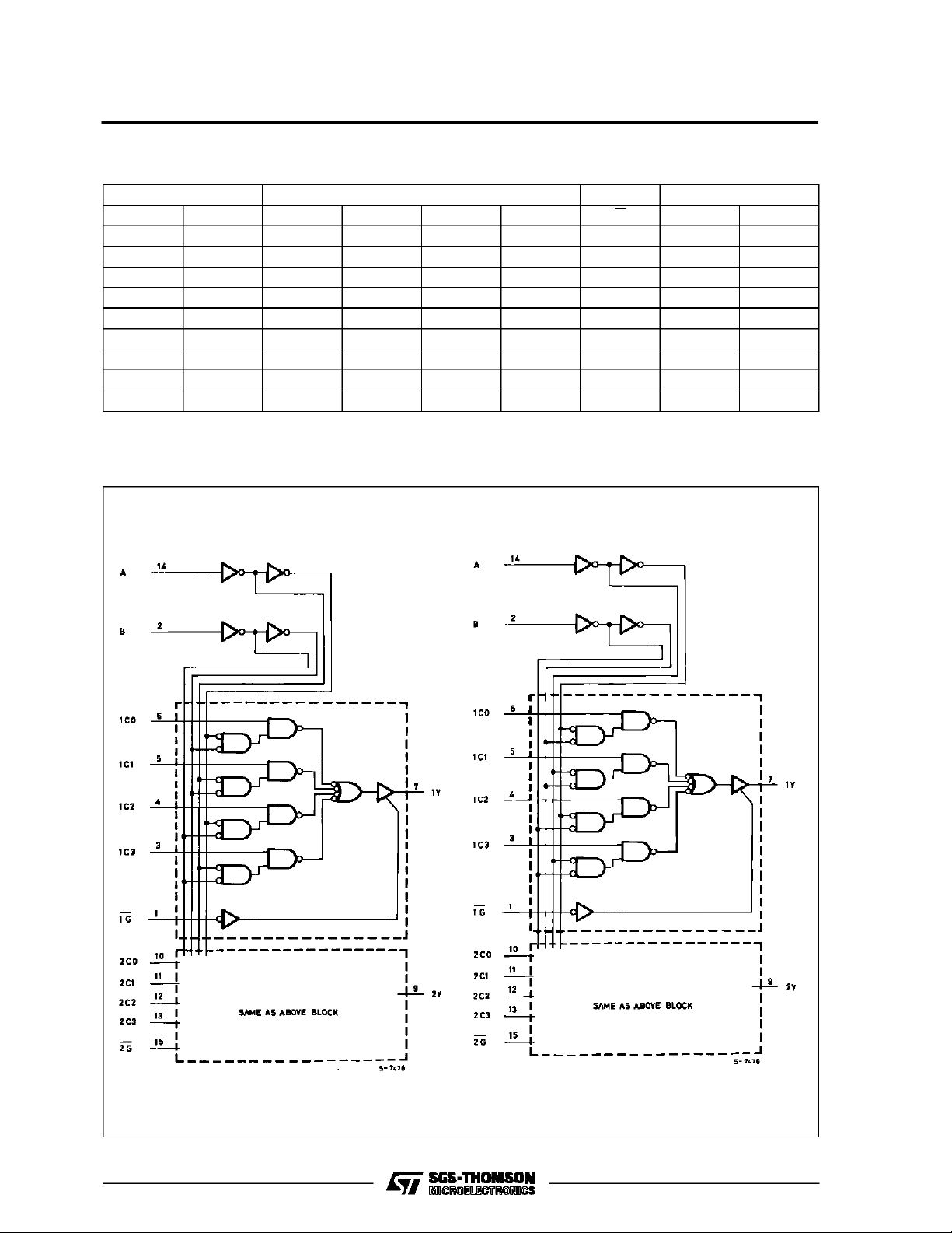
LOGIC DIAGRAM
HC153 HC253
C
1
C
2
C
3
G HC153 HC253
3/12
Page 4
M54/M74HC153 M54/M74HC253
ABSOLU TE M AXIMU M R AT INGS
Symbol Parameter Value Unit
V
CC
V
V
O
I
IK
I
OK
I
O
I
or I
CC
P
D
T
stg
T
L
AbsoluteMaximumRatings arethose values beyond whichdamagetothedevice mayoccur. Functional operation under these conditionisnotimplied.
(*)500 mW: ≅ 65oC derateto300 mWby 10mW/oC: 65oCto85oC
RECO MM ENDED OPERATI N G CO NDI TI O NS
Symbol Parameter Value Unit
V
CC
V
I
V
O
T
op
t
r,tf
Supply Voltage -0.5 to +7 V
DC Input Voltage -0.5 to VCC+ 0.5 V
I
DC Output Voltage -0.5 to VCC+ 0.5 V
DC Input Diode Current ± 20 mA
DC Output Diode Current ± 20 mA
DC Output Source Sink Current Per Output Pin ± 25 mA
DC VCCor Ground Current ± 50 mA
GND
Power Dissipation 500 (*) mW
Storage Temperature -65 to +150
Lead Temperature (10 sec) 300
Supply Voltage 2 to 6 V
Input Voltage 0 to V
Output Voltage 0 to V
Operating Temperature: M54HC Series
M74HC Series
CC
CC
-55 to +125
-40 to +85
Input Rise and Fall Time VCC= 2 V 0 to 1000 ns
V
= 4.5 V 0 to 500
CC
= 6 V 0 to 400
V
CC
o
C
o
C
V
V
o
C
o
C
4/12
Page 5

DC SPECIFICATIONS
Symbol Parameter
V
V
V
V
I
OZ
I
Note: 1. Appliedonlyfor M54/M74HC253
High Level Input
IH
Voltage
Low Level Input
IL
Voltage
High Level
OH
Output Voltage
Low Level Output
OL
Voltage
I
Input Leakage
I
Current
(1) 3 State Output
Off State Current
Quiescent Supply
CC
Current
M54/M 74HC1 53 M54/M7 4 HC 253
Test Conditions Value
T
=25oC
V
(V)
CC
A
54HC and 74HC
Min. Typ. Max. Min. Max. Min. Max.
2.0 1.5 1.5 1.5
4.5 3.15 3.15 3.15
6.0 4.2 4.2 4.2
2.0 0.5 0.5 0.5
4.5 1.35 1.35 1.35
6.0 1.8 1.8 1.8
2.0
4.5 4.4 4.5 4.4 4.4
6.0 5.9 6.0 5.9 5.9
4.5 I
6.0 I
2.0
4.5 0.0 0.1 0.1 0.1
6.0 0.0 0.1 0.1 0.1
4.5 I
6.0 I
6.0
6.0
=
V
I
IO=-20 µA
V
IH
or
V
IL
=-4.0 mA 4.18 4.31 4.13 4.10
O
=-5.2 mA 5.68 5.8 5.63 5.60
O
V
=
I
IO=20µA
V
IH
or
V
IL
= 4.0 mA 0.17 0.26 0.33 0.40
O
= 5.2 mA 0.18 0.26 0.33 0.40
O
VI=VCCor GND ±0.1 ±1 ±1 µA
V
I=VIH
or V
VO=VCCor GND
1.9 2.0 1.9 1.9
0.0 0.1 0.1 0.1
IL
6.0 VI=VCCor GND 4 40 80 mA
-40 to 85oC
74HC
-55 to 125oC
54HC
Unit
±0.5 ±5 ±10 µA
V
V
V
V
5/12
Page 6

M54/M74HC153 M54/M74HC253
AC ELECTRICAL CHARACTERISTICS (CL=50pF,Inputtr=tf=6ns)
Test Conditions Value
T
=25oC
Symbol Parameter
t
t
TLH
THL
Output Transition
Time
V
CC
(V)
2.0 30 75 95 110
4.5 8151922
A
54HC and 74HC
Min. Typ. Max. Min. Max. Min. Max.
6.0 7131619
t
PLH
t
PHL
Propagation
Delay Time
(Cn - Y)
t
t
PLH
PHL
Propagation
Delay Time
(A, B - Y)
t
t
PLH
PHL
Propagation
Delay Time
(G - Y)
t
PZL
t
PZH
Propagation
Delay Time (for
HC253) (G - Y)
t
PLZ
t
PHZ
Propagation
Delay Time (for
HC253) (G - Y)
C
C
PD
Input Capacitance 5 10 10 10 pF
IN
(*) Power Dissipation
2.0 48 115 145 175
4.5 15 23 29 35
6.0 12 20 25 30
2.0 68 150 190 225
4.5 20 30 38 45
6.0 16 26 32 38
2.0 30 85 105 130
4.5 10 17 21 26
6.0 9141822
2.0
RL=1KΩ
4.5 12 20 25 30
36 100 125 150
6.0 9172126
2.0
R
=1KΩ
L
4.5 11 20 25 30
22 100 125 150
6.0 9172126
58
Capacitance
(*) CPDisdefined as the value ofthe IC’sinternal equivalent capacitance which iscalculated from theoperating current consumption without load.
(Referto Test Circuit). Average opertingcurrent canbe obtained by thefollowingequation. ICC(opr) = CPD•VCC•fIN+ICC/4(per circuit)
-40 to 85oC
74HC
-55 to 125oC
54HC
Unit
ns
ns
ns
ns
ns
ns
pF
6/12
Page 7

SWITCHING CHARACTERISTICS TEST WAVEFORM
M54/M 74HC1 53 M54/M7 4 HC 253
TEST CIRCUIT ICC(Opr.)
7/12
Page 8

M54/M74HC153 M54/M74HC253
Plastic DIP16 (0.25) MECHANICAL DATA
DIM.
MIN. TYP. MAX. MIN. TYP. MAX.
a1 0.51 0.020
B 0.77 1.65 0.030 0.065
b 0.5 0.020
b1 0.25 0.010
D 20 0.787
E 8.5 0.335
e 2.54 0.100
e3 17.78 0.700
F 7.1 0.280
I 5.1 0.201
L 3.3 0.130
Z 1.27 0.050
mm inch
8/12
P001C
Page 9

M54/M 74HC1 53 M54/M7 4 HC 253
Ceramic DIP16/1 MECHANICAL DATA
DIM.
MIN. TYP. MAX. MIN. TYP. MAX.
A 20 0.787
B 7 0.276
D 3.3 0.130
E 0.38 0.015
e3 17.78 0.700
F 2.29 2.79 0.090 0.110
G 0.4 0.55 0.016 0.022
H 1.17 1.52 0.046 0.060
L 0.22 0.31 0.009 0.012
M 0.51 1.27 0.020 0.050
N 10.3 0.406
P 7.8 8.05 0.307 0.317
Q 5.08 0.200
mm inch
P053D
9/12
Page 10

M54/M74HC153 M54/M74HC253
SO16 (Narrow) MECHANICAL DATA
DIM.
MIN. TYP. MAX. MIN. TYP. MAX.
A 1.75 0.068
a1 0.1 0.2 0.004 0.007
a2 1.65 0.064
b 0.35 0.46 0.013 0.018
b1 0.19 0.25 0.007 0.010
C 0.5 0.019
c1 45° (typ.)
D 9.8 10 0.385 0.393
E 5.8 6.2 0.228 0.244
e 1.27 0.050
e3 8.89 0.350
F 3.8 4.0 0.149 0.157
G 4.6 5.3 0.181 0.208
L 0.5 1.27 0.019 0.050
M 0.62 0.024
S8°(max.)
mm inch
10/12
P013H
Page 11

M54/M 74HC1 53 M54/M7 4 HC 253
PLCC20 MECHANICAL DATA
DIM.
MIN. TYP. MAX. MIN. TYP. MAX.
A 9.78 10.03 0.385 0.395
B 8.89 9.04 0.350 0.356
D 4.2 4.57 0.165 0.180
d1 2.54 0.100
d2 0.56 0.022
E 7.37 8.38 0.290 0.330
e 1.27 0.050
e3 5.08 0.200
F 0.38 0.015
G 0.101 0.004
M 1.27 0.050
M1 1.14 0.045
mm inch
P027A
11/12
Page 12

M54/M74HC153 M54/M74HC253
Information furnishedis believed to be accurate and reliable. However, SGS-THOMSON Microelectronics assumes no responsability for the
consequences of useof such information norfor any infringementof patents orother rights of third partieswhich mayresults from its use. No
license is granted byimplication or otherwiseunder any patentor patent rightsofSGS-THOMSON Microelectronics.Specificationsmentioned
in thispublication are subjectto changewithout notice. This publication supersedes and replacesall information previously supplied.
SGS-THOMSON Microelectronicsproducts are not authorized foruse ascritical componentsin life supportdevices or systemswithout express
written approval of SGS-THOMSON Microelectonics.
1994SGS-THOMSON Microelectronics- All Rights Reserved
Australia -Brazil - France- Germany - HongKong - Italy - Japan - Korea - Malaysia- Malta - Morocco- The Netherlands-
Singapore -Spain - Sweden- Switzerland - Taiwan - Thailand - United Kingdom - U.S.A
SGS-THOMSON Microelectronics GROUP OFCOMPANIES
12/12
 Loading...