

Page 1
.HIGH SPEED
tPD= 15 ns(TYP.) ATVCC=5V
.LOWPOWER DISSIPATION
ICC=4µA(MAX.) AT TA=25°C
.HIGH NOISE IMMUNITY
V
NIH=VNIL
=28%VCC(MIN.)
.OUTPUT DRIVE CAPABILITY
10 LSTTLLOADS
.SYMMETRICALOUTPUT IMPEDANCE
IOH =IOL= 4 mA (MIN.)
.BALANCEDPROPAGATION DELAYS
t
PLH=tPHL
.WIDE OPERATING VOLTAGERANGE
VCC(OPR)= 2 V TO6 V
.PIN ANDFUNCTION COMPATIBLE
WITH 54/74LS151
DESCRIPTION
The M54/74HC151 is ahighspeedCMOS8CHANNEL MULTIPLEXER fabricated in silicon gate
C2MOStechnology.It hasthesamehighspeedperformance of LSTTL combined with true CMOS low
powerconsumption.Itprovides, inonepackage,the
ability to select one bit of data from up to eight
sources. The HC151 can be used as a universal
functiongenerator to generate any logic functionof
fourvariables. Outputs YandW arecomplementary
selectiondepends on the address inputs A, B and
C. Thestrobeinput mustbetaken low toenablethis
device, when the strobe is highW output is forced
highand consequently Y output goes low. Allinputs
are equipped with protection circuits against static
discharge and transient excess voltage.
M54HC151
M74HC151
8 CHANNEL MULTIPLEXER
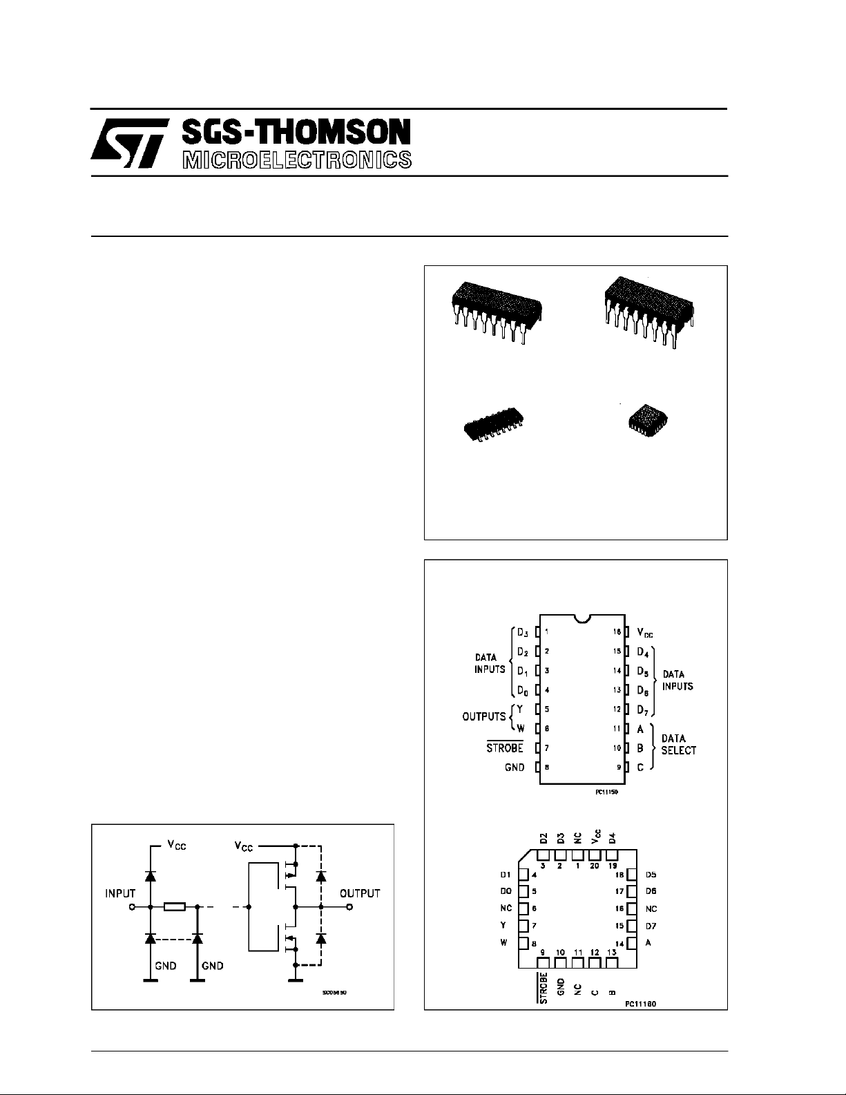
B1R
(PlasticPackage)
M1R
(MicroPackage)
ORDER CODES :
M54HC 151F1R M74H C151M1R
M74HC 151B1R M74HC1 51C1R
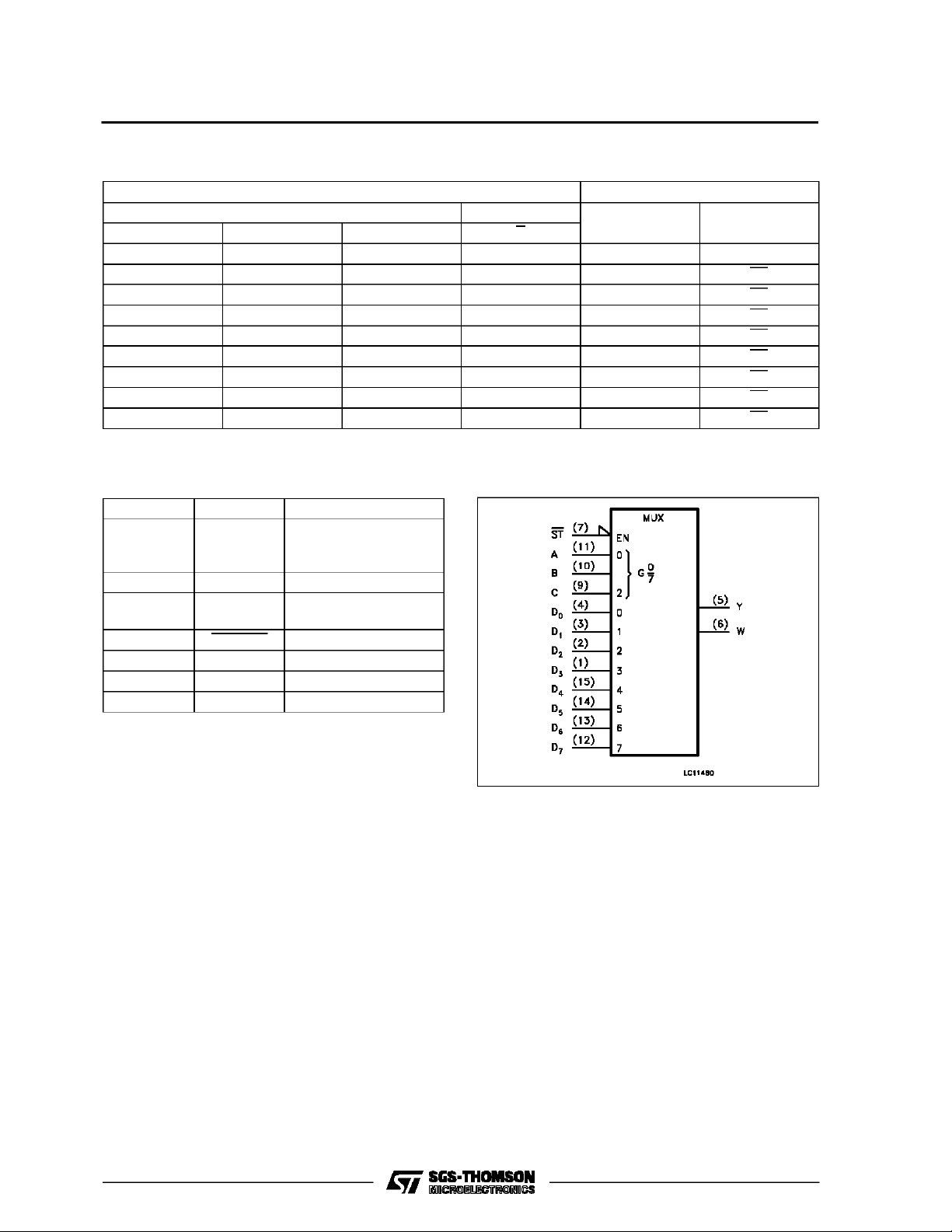
PIN CONNECTIONS (top view)
F1R
(CeramicPackage)
C1R
(Chip Carrier)
INPUT AND OUTPUT EQUIVALENT CIRCUIT
February 1993
NC =
No Internal
Connection
1/11
Page 2
M54/M74HC151
TRUTH TABLE
CBAS
XXXHLH
LLLLD0D0
L L H L D1 D1
LHLLD2D2
LHHLD3D3
H L L L D4 D4
H L H L D5 D5
H H L L D6 D6
H H H L D7 D7
INPUTS OUTPUTS
SELECT STROBE
YW
PIN DESCRIPTION
PIN No SYMBOL NAME AND FUNCTION
4, 3, 2, 1,
15, 14, 13,
12
5 y Multiplexer Output
6 w Complementary
7 STROBE StrobeInput
11, 10, 9 A, B, C Select Inputs
8 GND Ground (0V)
16 V
D0 to D7 Multiplexer Inputs
Multiplexer Output
CC
Positive Supply Voltage
IEC LOGIC SYMBOL
2/11
Page 3
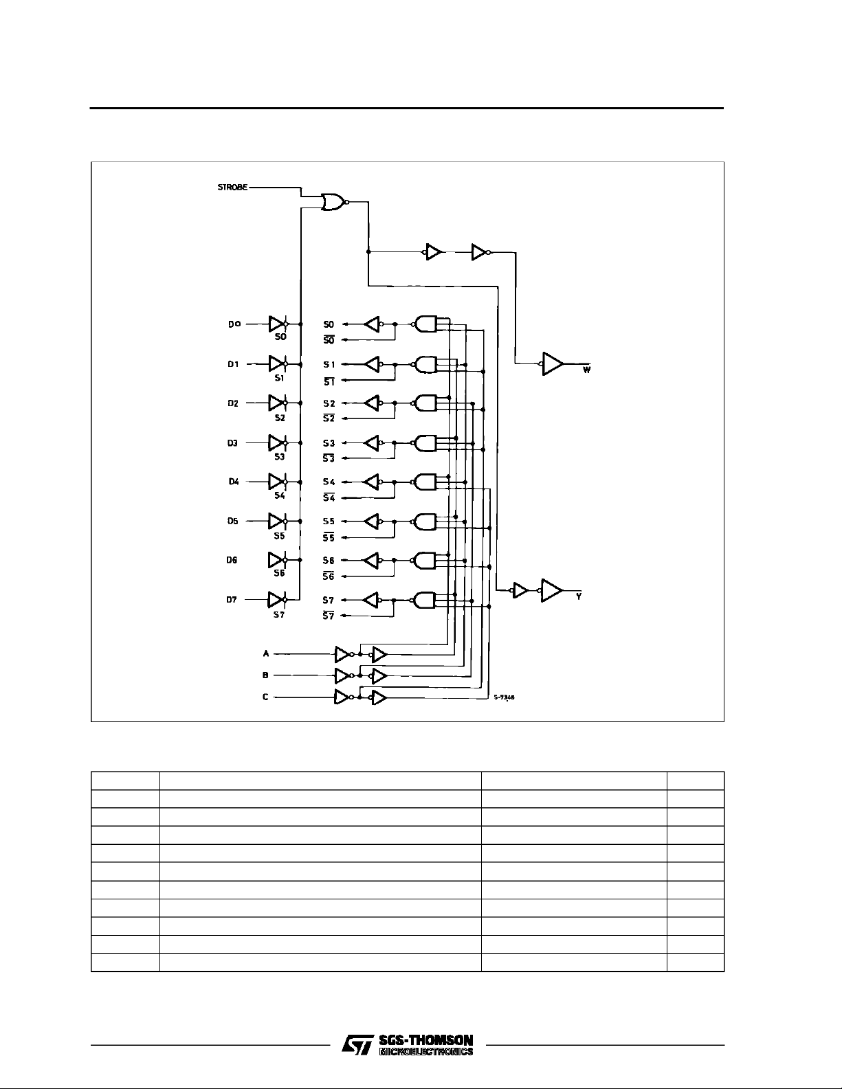
LOGI C DIAGRAM
M54/M74HC151
ABSOLU TE MAXIMUM RATINGS
Symbol Parameter Value Unit
V
CC
V
V
O
I
IK
I
OK
I
O
or I
I
CC
P
D
T
stg
T
AbsoluteMaximumRatingsarethosevalues beyond whichdamage tothedevicemayoccur.Functional operation under these conditionisnotimplied.
(*)500 mW:≅ 65oC derateto300mWby 10mW/oC: 65oCto85oC
Supply Voltage -0.5 to +7 V
DC Input Voltage -0.5 to VCC+ 0.5 V
I
DC Output Voltage -0.5 to VCC+ 0.5 V
DC Input Diode Current ± 20 mA
DC Output Diode Current ± 20 mA
DC Output Source Sink Current Per Output Pin ± 25 mA
DC VCCor Ground Current ± 50 mA
GND
Power Dissipation 500 (*) mW
Storage Temperature -65 to +150
Lead Temperature (10 sec) 300
L
o
C
o
C
3/11
Page 4
M54/M74HC151
RECO MM ENDED OPERAT I N G C O NDITIONS
Symbol Parameter Value Unit
V
V
V
T
t
r,tf
DC SPECIFICA TIONS
Symbol Parameter
V
IH
V
V
OH
V
OL
I
I
CC
Supply Voltage 2 to 6 V
CC
Input Voltage 0 to V
I
Output Voltage 0 to V
O
Operating Temperature: M54HC Series
op
M74HC Series
CC
CC
-55 to +125
-40 to +85
Input Rise and Fall Time VCC= 2 V 0 to 1000 ns
V
= 4.5 V 0 to 500
CC
V
= 6 V 0 to 400
CC
Test Conditions Value
V
(V)
CC
=25oC
T
A
54HC and 74HC
-40 to 85oC
74HC
-55 to 125oC
Min. Typ. Max. Min. Max. Min. Max.
High Level Input
Voltage
2.0 1.5 1.5 1.5
4.5 3.15 3.15 3.15
6.0 4.2 4.2 4.2
Low Level Input
IL
Voltage
2.0 0.5 0.5 0.5
4.5 1.35 1.35 1.35
6.0 1.8 1.8 1.8
High Level
Output Voltage
Low Level Output
Voltage
Input Leakage
I
Current
Quiescent Supply
2.0
V
=
I
4.5 4.4 4.5 4.4 4.4
6.0 5.9 6.0 5.9 5.9
4.5 I
6.0 I
2.0
4.5 0.0 0.1 0.1 0.1
6.0 0.0 0.1 0.1 0.1
4.5 I
6.0 I
6.0
IO=-20 µA
V
IH
or
V
IL
=-4.0 mA 4.18 4.31 4.13 4.10
O
=-5.2 mA 5.68 5.8 5.63 5.60
O
V
=
I
IO=20µA
V
IH
or
V
IL
= 4.0 mA 0.17 0.26 0.33 0.40
O
= 5.2 mA 0.18 0.26 0.33 0.40
O
VI=VCCor GND ±0.1 ±1 ±1 µA
1.9 2.0 1.9 1.9
0.0 0.1 0.1 0.1
6.0 VI=VCCor GND 4 40 80 µA
Current
54HC
V
V
o
C
o
C
Unit
V
V
V
V
4/11
Page 5
M54/M74HC151
AC ELECTRICAL CHARACTERISTICS (CL=50pF,Inputtr=tf=6ns)
Test Conditions Value
T
=25oC
Symbol Parameter
t
t
TLH
THL
Output Transition
Time
V
CC
(V)
2.0 30 75 95 110
4.5 8151922
A
54HC and 74HC
Min. Typ. Max. Min. Max. Min. Max.
6.0 7131619
t
PLH
t
PHL
Propagation
Delay Time
(D - W)
t
t
PLH
PHL
Propagation
Delay Time
(D - Y)
t
t
PLH
PHL
Propagation
Delay Time
(STROBE - W)
t
PLH
t
PHL
Propagation
Delay Time
(STROBE - Y)
t
PLH
t
PHL
Propagation
Delay Time
(A, B, C - W)
t
t
PLH
PHL
Propagation
Delay Time
(A, B, C - Y)
C
C
PD
Input Capacitance 5 10 10 10 pF
IN
(*) Power Dissipation
2.0 56 130 165 190
4.5 16 26 33 38
6.0 14 22 28 32
2.0 56 130 165 190
4.5 16 26 33 38
6.0 14 22 28 32
2.0 30 85 105 125
4.5 10 17 21 25
6.0 9141821
2.0 30 85 105 125
4.5 10 17 21 25
6.0 9141821
2.0 72 160 200 235
4.5 20 32 40 47
6.0 17 27 34 40
2.0 72 160 200 235
4.5 20 32 40 47
6.0 17 27 34 40
63
Capacitance
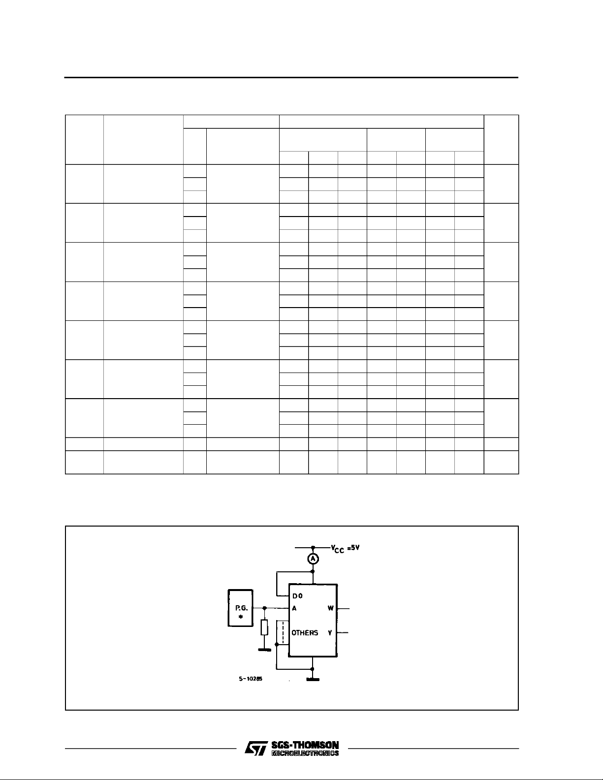
(*) CPDisdefined as the valueofthe IC’s internal equivalent capacitance whichis calculated from the operating currentconsumption without load.
(RefertoTest Circuit).Average operting current can be obtained bythefollowingequation. ICC(opr) = CPD•VCC•fIN+I
-40 to 85oC
74HC
-55 to 125oC
54HC
CC
Unit
ns
ns
ns
ns
ns
ns
ns
pF
TEST CIRCUIT ICC(Opr.)
* INPUTWAVEFORMISTHESAME AS THAT IN CASE OFSWITCHINGCHARACTERISTICSTEST.
5/11
Page 6

M54/M74HC151
SWITCHING CHARACTERISTICS TEST WAVEFORM
6/11
Page 7

Plastic DIP16 (0.25) MECHANICAL DATA
M54/M74HC151
DIM.
MIN. TYP. MAX. MIN. TYP. MAX.
a1 0.51 0.020
B 0.77 1.65 0.030 0.065
b 0.5 0.020
b1 0.25 0.010
D 20 0.787
E 8.5 0.335
e 2.54 0.100
e3 17.78 0.700
F 7.1 0.280
I 5.1 0.201
L 3.3 0.130
Z 1.27 0.050
mm inch
P001C
7/11
Page 8

M54/M74HC151
Ceramic DIP16/1 MECHANICAL DATA
DIM.
MIN. TYP. MAX. MIN. TYP. MAX.
A 20 0.787
B 7 0.276
D 3.3 0.130
E 0.38 0.015
e3 17.78 0.700
F 2.29 2.79 0.090 0.110
G 0.4 0.55 0.016 0.022
H 1.17 1.52 0.046 0.060
L 0.22 0.31 0.009 0.012
M 0.51 1.27 0.020 0.050
N 10.3 0.406
P 7.8 8.05 0.307 0.317
Q 5.08 0.200
mm inch
8/11
P053D
Page 9

SO16 (Narrow) MECHANICAL DATA
M54/M74HC151
DIM.
MIN. TYP. MAX. MIN. TYP. MAX.
A 1.75 0.068
a1 0.1 0.2 0.004 0.007
a2 1.65 0.064
b 0.35 0.46 0.013 0.018
b1 0.19 0.25 0.007 0.010
C 0.5 0.019
c1 45° (typ.)
D 9.8 10 0.385 0.393
E 5.8 6.2 0.228 0.244
e 1.27 0.050
e3 8.89 0.350
F 3.8 4.0 0.149 0.157
G 4.6 5.3 0.181 0.208
L 0.5 1.27 0.019 0.050
M 0.62 0.024
S8°(max.)
mm inch
P013H
9/11
Page 10
M54/M74HC151
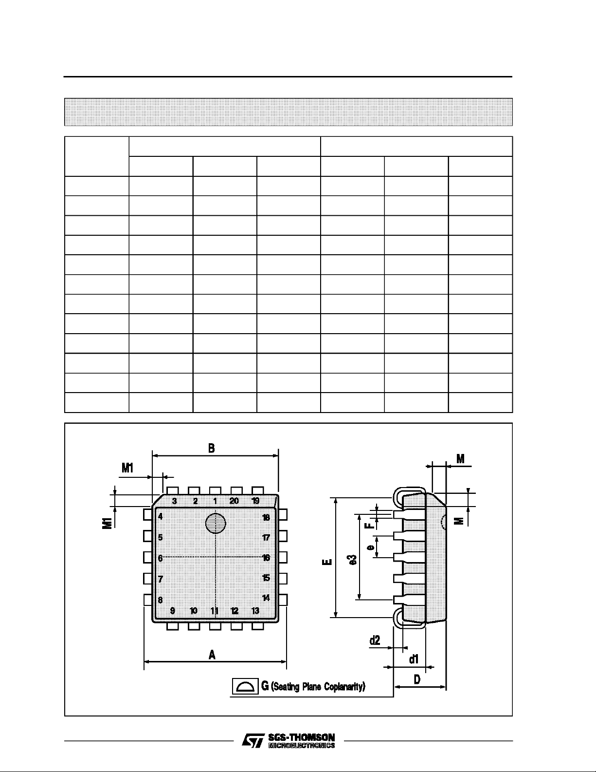
PLCC20 MECHANICAL DATA
DIM.
MIN. TYP. MAX. MIN. TYP. MAX.
A 9.78 10.03 0.385 0.395
B 8.89 9.04 0.350 0.356
D 4.2 4.57 0.165 0.180
d1 2.54 0.100
d2 0.56 0.022
E 7.37 8.38 0.290 0.330
e 1.27 0.050
e3 5.08 0.200
F 0.38 0.015
G 0.101 0.004
M 1.27 0.050
M1 1.14 0.045
mm inch
10/11
P027A
Page 11

M54/M74HC151
Information furnished is believed to be accurate and reliable. However, SGS-THOMSON Microelectronics assumes no responsability for the
consequences of use of such information nor for any infringement of patents or other rights of third parties which may results from its use. No
license is granted byimplication or otherwise under any patent or patentrights of SGS-THOMSON Microelectronics. Specificationsmentioned
in this publication are subject to change without notice. This publication supersedes and replaces all information previously supplied.
SGS-THOMSON Microelectronicsproductsarenotauthorizedforuse ascriticalcomponentsinlifesupportdevicesorsystemswithoutexpress
written approval of SGS-THOMSON Microelectonics.
1994 SGS-THOMSON Microelectronics - All Rights Reserved
Australia - Brazil - France - Germany - Hong Kong - Italy - Japan - Korea - Malaysia - Malta - Morocco - The Netherlands -
Singapore -Spain - Sweden- Switzerland -Taiwan - Thailand - UnitedKingdom - U.S.A
SGS-THOMSON Microelectronics GROUP OF COMPANIES
11/11
 Loading...