

Page 1
DUAL 2 TO 4 DECODER/DEMULTIPLEXER
.HIGH SPEED
tPD= 12 ns(TYP.) AT VCC=5V
.LOWPOWER DISSIPATION
ICC=4µA(MAX.) AT TA=25°C
.HIGH NOISE IMMUNITY
V
NIH=VNIL
=28%VCC(MIN.)
.OUTPUT DRIVE CAPABILITY
10 LSTTL LOADS
.SYMMETRICALOUTPUT IMPEDANCE
|IOH|=IOL=4 mA (MIN.)
.BALANCEDPROPAGATION DELAYS
t
PLH=tPHL
.WIDE OPERATING VOLTAGERANGE
VCC(OPR)= 2 V TO 6 V
.PIN AND FUNCTION COMPATIBLE
WITH 54/74LS139
M54HC139
M74HC139
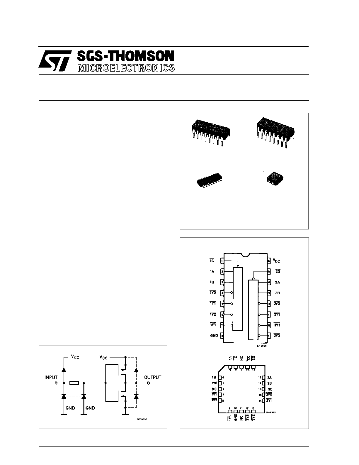
B1R
(PlasticPackage)
M1R
(MicroPackage)
ORDER CODES :
M54HC 139F1R M74H C139M1R
M74HC 139B1R M74HC1 39C1R
F1R
(CeramicPackage)
C1R
(Chip Carrier)
DESCRIPTION
The M54/74HC139 is a high speed CMOS DUAL
TWO LINE TO FOUR LINE DECODER/DEMULTIPLEXER fabricatedin silicon gate C2MOS technology. It has the same high speed performance of
LSTTL combined with true CMOS low power consumption.The activelow enableinput can be used
for gating or as a data input for demultiplexing applications. While the enable input is held high, all
four outputs are high independently of the other inputs.Allinputs are equipped with protectioncircuits
against static discharge and transient excess voltage.
INPUT AND OUTPUT EQUIVALENT CIRCUIT
PIN CONNECTIONS (top view)
February 1993
NC =
No Internal
Connection
1/9
Page 2
M54/M74HC139
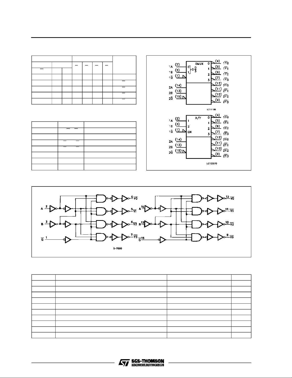
TRUTH TABLE
INPUTS OUTPUTS
ENABLE SELECT
GBA
Y
0Y1Y2Y3
H X X H H H H NONE
L LLLHHH Y
LLHHLHHY
LHLHHLHY
L HHHHHL Y
SELECTED
OUTPUT
PIN DESCRIPTION
PIN No SYMBOL NAME AND FUNCTION
1, 15 1G, 2G Enable Inputs
2, 3 1A, 1B Address Inputs
4, 5, 6, 7 1Y
12, 11, 10, 9 2Y
to 1Y3Outputs
0
to 2Y3Outputs
0
14, 13 2A, 2B Address Inputs
8 GND Ground(0V)
16 V
CC
Positive Supply Voltage
SCHEM ATIC CIRCUIT
IEC LOGIC SYMBOL
0
1
2
3
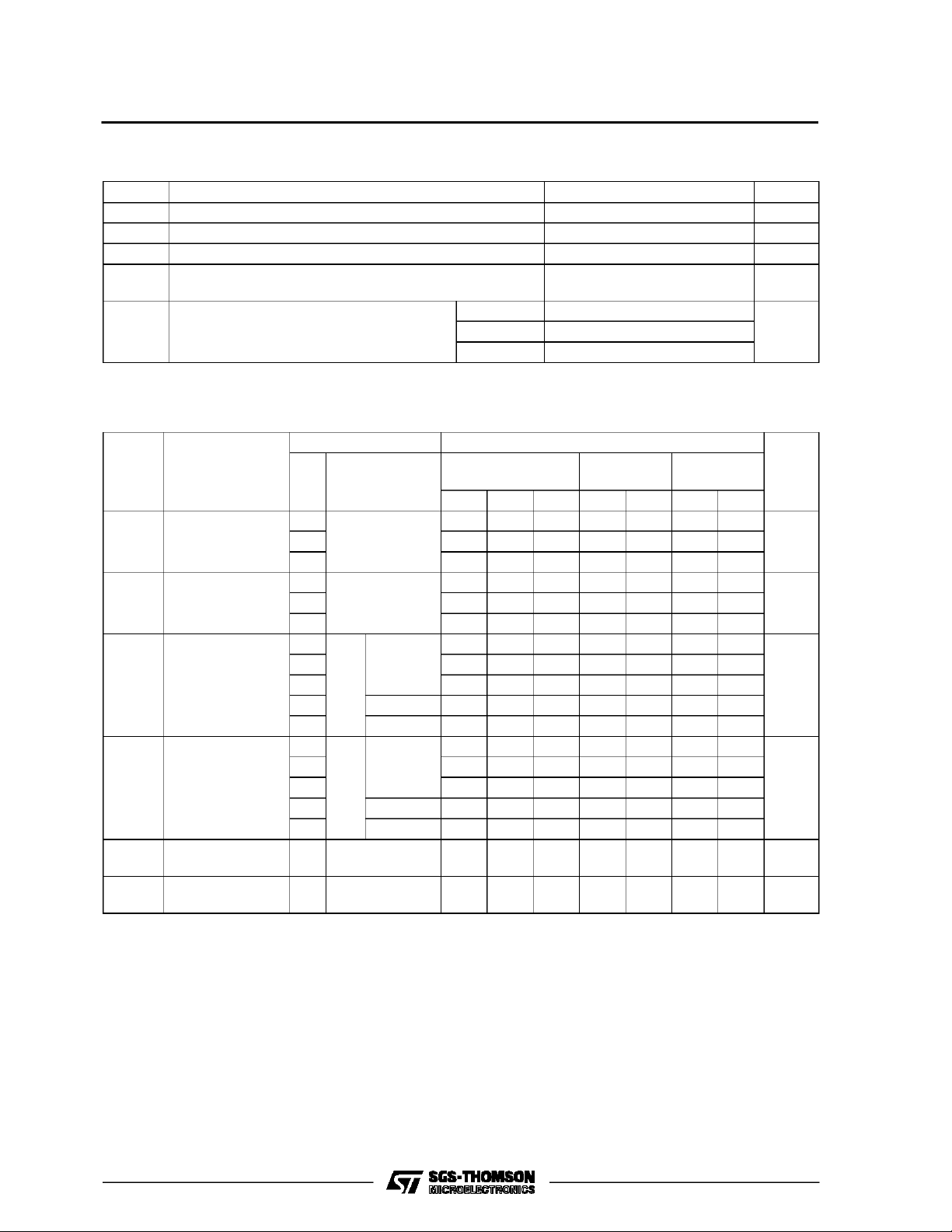
ABSOLU TE M AXIMU M R AT INGS
Symbol Parameter Value Unit
V
CC
V
V
O
I
IK
I
OK
I
O
or I
I
CC
P
D
T
stg
T
L
AbsoluteMaximumRatingsarethosevalues beyond whichdamagetothedevicemayoccur.Functionaloperationunder these conditionisnotimplied.
(*)500 mW:≅ 65oC derateto300mWby 10mW/oC: 65oCto85oC
2/9
Supply Voltage -0.5 to +7 V
DC Input Voltage -0.5 to VCC+ 0.5 V
I
DC Output Voltage -0.5 to VCC+ 0.5 V
DC Input Diode Current ± 20 mA
DC Output Diode Current ± 20 mA
DC Output Source Sink Current Per Output Pin ± 25 mA
DC VCCor Ground Current ± 50 mA
GND
Power Dissipation 500 (*) mW
Storage Temperature -65 to +150
Lead Temperature (10 sec) 300
o
C
o
C
Page 3
M54/M74HC139
RECO MM ENDED OPERAT I N G C ONDITI ONS
Symbol Parameter Value Unit
V
V
V
T
t
r,tf
DC SPECIFICATIONS
Symbol Parameter
V
IH
V
V
OH
V
OL
I
I
CC
Supply Voltage 2 to 6 V
CC
Input Voltage 0 to V
I
Output Voltage 0 to V
O
Operating Temperature: M54HC Series
op
M74HC Series
CC
CC
-55 to +125
-40 to +85
Input Rise and Fall Time VCC= 2 V 0 to 1000 ns
V
= 4.5 V 0 to 500
CC
V
= 6 V 0 to 400
CC
Test Conditions Value
V
(V)
CC
=25oC
T
A
54HC and 74HC
-40 to 85oC
74HC
-55 to 125oC
Min. Typ. Max. Min. Max. Min. Max.
High Level Input
Voltage
2.0 1.5 1.5 1.5
4.5 3.15 3.15 3.15
6.0 4.2 4.2 4.2
Low Level Input
IL
Voltage
2.0 0.5 0.5 0.5
4.5 1.35 1.35 1.35
6.0 1.8 1.8 1.8
High Level
Output Voltage
Low Level Output
Voltage
Input Leakage
I
Current
Quiescent Supply
2.0
V
=
I
4.5 4.4 4.5 4.4 4.4
6.0 5.9 6.0 5.9 5.9
4.5 I
6.0 I
2.0
4.5 0.0 0.1 0.1 0.1
6.0 0.0 0.1 0.1 0.1
4.5 I
6.0 I
6.0
IO=-20 µA
V
IH
or
V
IL
=-4.0 mA 4.18 4.31 4.13 4.10
O
=-5.2 mA 5.68 5.8 5.63 5.60
O
V
=
I
IO=20µA
V
IH
or
V
IL
= 4.0 mA 0.17 0.26 0.33 0.40
O
= 5.2 mA 0.18 0.26 0.33 0.40
O
VI=VCCor GND ±0.1 ±1 ±1 µA
1.9 2.0 1.9 1.9
0.0 0.1 0.1 0.1
6.0 VI=VCCor GND 4 40 80 µA
Current
54HC
V
V
o
C
o
C
Unit
V
V
V
V
3/9
Page 4

M54/M74HC139
AC ELECTRICAL CHARACTERISTICS (CL=50pF,Inputtr=tf=6ns)
Test Conditions Value
T
=25oC
Symbol Parameter
t
t
TLH
THL
Output Transition
Time
V
CC
(V)
2.0 30 75 95 110
4.5 8151922
A
54HC and 74HC
Min. Typ. Max. Min. Max. Min. Max.
6.0 7131619
t
PLH
t
PHL
Propagation
Delay Time
(A, B - Y)
t
t
PLH
PHL
Propagation
Delay Time
(G - Y)
C
C
PD
Input Capacitance 5 10 10 10 pF
IN
(*) Power Dissipation
2.0 45 130 165 195
4.5 15 26 33 39
6.0 13 22 28 33
2.0 39 110 140 165
4.5 13 22 28 33
6.0 11 19 24 28
46
Capacitance
(*) CPDisdefined as the valueofthe IC’s internal equivalent capacitance whichis calculated fromthe operating current consumption withoutload.
(RefertoTest Circuit).Average opertingcurrentcanbe obtained bythefollowingequation. ICC(opr) = CPD•VCC•fIN+I
-40 to 85oC
74HC
-55 to 125oC
54HC
CC
Unit
ns
ns
ns
pF
SWITCHING CHARACTERISTICS TEST CIRCUIT
TEST CIRCUIT ICC(Opr.)
INPUT WAVEFORM IS THE SAME AS THAT IN CASE OF
SWITCHING CHARACTERISTICSTEST.
4/9
Page 5

Plastic DIP16 (0.25) MECHANICAL DATA
M54/M74HC139
DIM.
MIN. TYP. MAX. MIN. TYP. MAX.
a1 0.51 0.020
B 0.77 1.65 0.030 0.065
b 0.5 0.020
b1 0.25 0.010
D 20 0.787
E 8.5 0.335
e 2.54 0.100
e3 17.78 0.700
F 7.1 0.280
I 5.1 0.201
L 3.3 0.130
Z 1.27 0.050
mm inch
P001C
5/9
Page 6

M54/M74HC139
Ceramic DIP16/1 MECHANICAL DATA
DIM.
MIN. TYP. MAX. MIN. TYP. MAX.
A 20 0.787
B 7 0.276
D 3.3 0.130
E 0.38 0.015
e3 17.78 0.700
F 2.29 2.79 0.090 0.110
G 0.4 0.55 0.016 0.022
H 1.17 1.52 0.046 0.060
L 0.22 0.31 0.009 0.012
M 0.51 1.27 0.020 0.050
N 10.3 0.406
P 7.8 8.05 0.307 0.317
Q 5.08 0.200
mm inch
6/9
P053D
Page 7

SO16 (Narrow) MECHANICAL DATA
M54/M74HC139
DIM.
MIN. TYP. MAX. MIN. TYP. MAX.
A 1.75 0.068
a1 0.1 0.2 0.004 0.007
a2 1.65 0.064
b 0.35 0.46 0.013 0.018
b1 0.19 0.25 0.007 0.010
C 0.5 0.019
c1 45° (typ.)
D 9.8 10 0.385 0.393
E 5.8 6.2 0.228 0.244
e 1.27 0.050
e3 8.89 0.350
F 3.8 4.0 0.149 0.157
G 4.6 5.3 0.181 0.208
L 0.5 1.27 0.019 0.050
M 0.62 0.024
S8°(max.)
mm inch
P013H
7/9
Page 8

M54/M74HC139
PLCC20 MECHANICAL DATA
DIM.
MIN. TYP. MAX. MIN. TYP. MAX.
A 9.78 10.03 0.385 0.395
B 8.89 9.04 0.350 0.356
D 4.2 4.57 0.165 0.180
d1 2.54 0.100
d2 0.56 0.022
E 7.37 8.38 0.290 0.330
e 1.27 0.050
e3 5.08 0.200
F 0.38 0.015
G 0.101 0.004
M 1.27 0.050
M1 1.14 0.045
mm inch
8/9
P027A
Page 9

M54/M74HC139
Information furnished is believed to be accurate and reliable. However, SGS-THOMSON Microelectronics assumes no responsability for the
consequences of use of such information nor for any infringement of patents or other rights of third parties which may results from its use. No
license is granted byimplication or otherwise under any patent or patentrights of SGS-THOMSON Microelectronics. Specificationsmentioned
in this publication are subject to change without notice. This publication supersedes and replaces all information previously supplied.
SGS-THOMSON Microelectronicsproductsarenotauthorizedforuse ascriticalcomponentsinlifesupportdevicesorsystemswithoutexpress
written approval of SGS-THOMSON Microelectonics.
1994 SGS-THOMSON Microelectronics - All Rights Reserved
Australia - Brazil - France - Germany - Hong Kong - Italy - Japan - Korea - Malaysia - Malta - Morocco - The Netherlands -
Singapore -Spain - Sweden- Switzerland -Taiwan - Thailand - UnitedKingdom - U.S.A
SGS-THOMSON Microelectronics GROUP OF COMPANIES
9/9
 Loading...