

Page 1
.HIGH SPEED
tPD= 13 ns(TYP.) at VCC=5V
.LOWPOWERDISSIPATION
ICC=1µA(MAX.) at TA=25°C
.HIGH NOISEIMMUNITY
V
NIH=VNIL
=28%VCC(MIN.)
.OUTPUT DRIVE CAPABILITY
10 LSTTL LOADS
.SYMMETRICALOutpuT IMPEDANCE
|IOH|=IOL=4 mA(MIN.)
.BALANCEDPROPAGATION DELAYS
t
PLH=tPHL
.WIDE OPERATINGVOLTAGE RANGE
VCC(OPR)= 2V to 6 V
.PIN ANDFUNCTION COMPATIBLE
WITH 54/74LS133
M54HC133
M74HC133
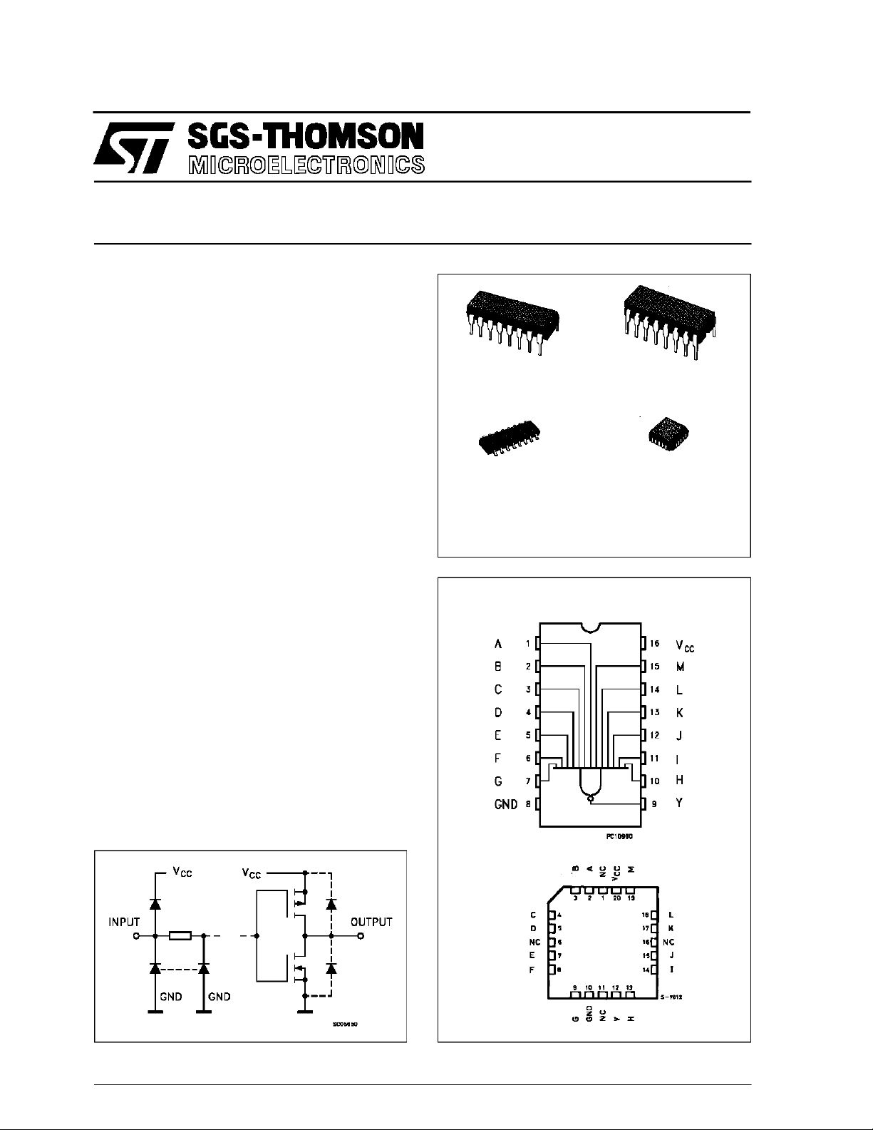
13 INPUT NAND GATE
B1R
(PlasticPackage)
M1R
(MicroPackage)
ORDER CODES :
M54HC 133F1R M74H C133M1R
M74HC 133B1R M74HC1 33C1R
F1R
(CeramicPackage)
C1R
(Chip Carrier)
DESCRIPTION
The M54/74HC133 is a high speed CMOS 13INPUT NAND GATE fabricated in silicon gate
C2MOStechnology. Ithasthesamehighspeedperformance of LSTTL combined with true CMOS low
powerconsumption.
The internal circuitiscomposed of 7 stagesincluding buffer output, which gives high noise immunity
and stable output.All inputs are equipped with protectioncircuits againststaticdischarge and transient
excess voltage.
INPUT AND OUTPUT EQUIVALENT CIRCUIT
PIN CONNECTIONS(top view)
NC =
No Internal
Connection
October 1992
1/10
Page 2
M54/M74HC133
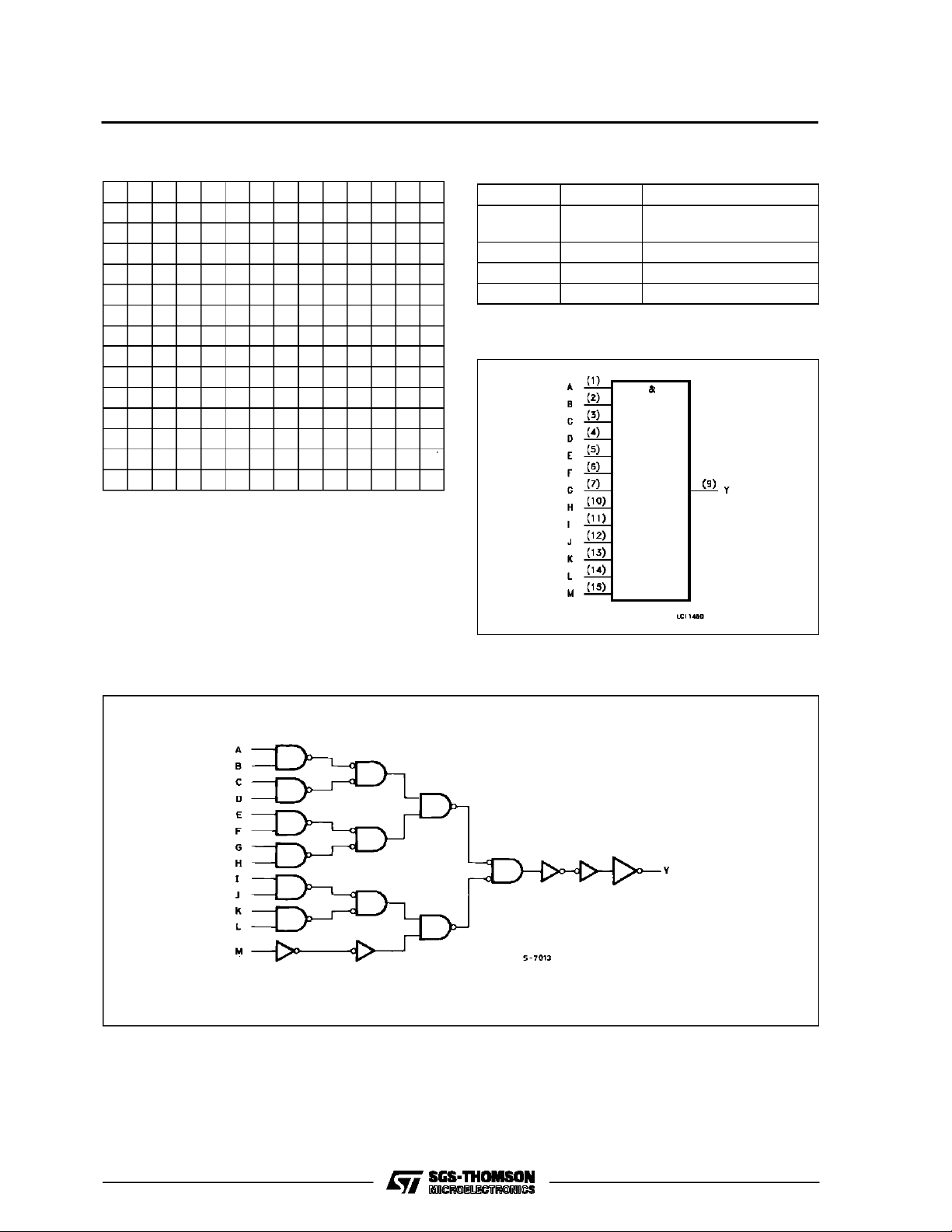
TRUTH TABLE
ABCDEFGH I JKLMY
LXXXXXXXXXXXXH
XLXXXXXXXXXXXH
XXLXXXXXXXXXXH
XXXLXXXXXXXXXH
XXXXLXXXXXXXXH
XXXXXLXXXXXXXH
XXXXXXLXXXXXXH
XXXXXXXLXXXXXH
XXXXXXXXLXXXXH
XXXXXXXXXLXXXH
XXXXXXXXXXLXXH
XXXXXXXXXXXLXH
XXXXXXXXXXXXLH
HHHHHHHHHHHHHL
X:Don’t Care
PIN DESCRIPTION
PIN No SYMBOL NAME AND FUNCTION
1to7,
10 to 15
9 Y Data Output
8 GND Ground (0V)
16 V
AtoG,
HtoM
CC
Data Inputs
Positive Supply Voltage
IEC LOGIC SYMBOL
LOGI C DIAGRAM (1 / 2 Packag e)
2/10
Page 3
M54/M74HC133
ABSOLU TE MAXIMU M RAT INGS
Symbol Parameter Value Unit
V
CC
V
V
O
I
IK
I
OK
I
O
I
or I
CC
P
D
T
stg
T
AbsoluteMaximumRatingsarethose values beyondwhichdamage tothedevicemayoccur. Functionaloperationunder these conditionisnotimplied.
(*)500 mW: ≅ 65oC derateto300mWby 10mW/oC: 65oCto85oC
RECO MM ENDED OPERATI N G CONDI TIONS
Symbol Parameter Value Unit
V
CC
V
I
V
O
T
op
t
r,tf
Supply Voltage -0.5 to +7 V
DC Input Voltage -0.5 to VCC+ 0.5 V
I
DC Output Voltage -0.5 to VCC+ 0.5 V
DC Input Diode Current ± 20 mA
DC Output Diode Current ± 20 mA
DC Output Source Sink Current Per Output Pin ± 25 mA
DC VCCor Ground Current ± 50 mA
GND
Power Dissipation 500 (*) mW
Storage Temperature -65 to +150
Lead Temperature (10 sec) 300
L
Supply Voltage 2 to 6 V
Input Voltage 0 to V
Output Voltage 0 to V
Operating Temperature: M54HC Series
M74HC Series
CC
CC
-55 to +125
-40 to +85
Input Rise and Fall Time VCC= 2 V 0 to 1000 ns
V
= 4.5 V 0 to 500
CC
= 6 V 0 to 400
V
CC
o
C
o
C
V
V
o
C
o
C
3/10
Page 4

M54/M74HC133
DC SPECIFICATIO NS
Symbol Parameter
V
V
V
V
I
High Level Input
IH
Voltage
Low Level Input
IL
Voltage
High Level
OH
Output Voltage
Low Level Output
OL
Voltage
I
Input Leakage
I
Current
Quiescent Supply
CC
Current
Test Conditions Value
V
(V)
CC
=25oC
A
54HC and 74HC
Min. Typ. Max. Min. Max. Min. Max.
-40 to 85oC
74HC
-55 to 125oC
54HC
Unit
T
2.0 1.5 1.5 1.5
4.5 3.15 3.15 3.15
6.0 4.2 4.2 4.2
2.0 0.5 0.5 0.5
4.5 1.35 1.35 1.35
6.0 1.8 1.8 1.8
2.0
4.5 4.4 4.5 4.4 4.4
6.0 5.9 6.0 5.9 5.9
4.5 I
6.0 I
2.0
4.5 0.0 0.1 0.1 0.1
6.0 0.0 0.1 0.1 0.1
4.5 I
6.0 I
6.0
=
V
I
IO=-20 µA
V
IH
or
V
IL
=-4.0 mA 4.18 4.31 4.13 4.10
O
=-5.2 mA 5.68 5.8 5.63 5.60
O
V
=
I
IO=20µA
V
IH
or
V
IL
= 4.0 mA 0.17 0.26 0.33 0.40
O
= 5.2 mA 0.18 0.26 0.33 0.40
O
VI=VCCor GND ±0.1 ±1 ±1 µA
1.9 2.0 1.9 1.9
0.0 0.1 0.1 0.1
6.0 VI=VCCor GND 1 10 20 µA
V
V
V
V
4/10
Page 5

M54/M74HC133
AC ELECTRICAL CHARACTERISTICS (CL=50pF,Inputtr=tf=6ns)
Test Conditions Value
T
=25oC
Symbol Parameter
t
t
TLH
THL
Output Transition
Time
V
CC
(V)
2.0 30 75 95 110
4.5 8151922
A
54HC and 74HC
Min. Typ. Max. Min. Max. Min. Max.
6.0 7131619
t
PLH
t
PHL
Propagation
Delay Time
2.0 42 130 165 195
4.5 16 26 33 39
6.0 14 22 28 33
C
C
PD
Input Capacitance 5 10 10 10 pF
IN
(*) Power Dissipation
29
Capacitance
(*) CPDisdefined as the value ofthe IC’sinternal equivalent capacitance whichis calculated fromthe operatingcurrent consumption without load.
(Referto Test Circuit). Average operting current canbe obtained bythe followingequation. ICC(opr) = CPD•VCC•fIN+I
SWITCHING CHARACTERISTICS TEST CIRCUIT
-40 to 85oC
74HC
-55 to 125oC
54HC
CC
Unit
ns
ns
pF
TEST CIRCUIT ICC(Opr.)
INPUT WAVEFORMIS THE SAMEAS THAT INCASE OF SWITCHINGCHARACTERISTICS TEST.
5/10
Page 6

M54/M74HC133
Plastic DIP16 (0.25) MECHANICAL DATA
DIM.
MIN. TYP. MAX. MIN. TYP. MAX.
a1 0.51 0.020
B 0.77 1.65 0.030 0.065
b 0.5 0.020
b1 0.25 0.010
D 20 0.787
E 8.5 0.335
e 2.54 0.100
e3 17.78 0.700
F 7.1 0.280
I 5.1 0.201
L 3.3 0.130
Z 1.27 0.050
mm inch
6/10
P001C
Page 7

Ceramic DIP16/1 MECHANICAL DATA
M54/M74HC133
DIM.
MIN. TYP. MAX. MIN. TYP. MAX.
A 20 0.787
B 7 0.276
D 3.3 0.130
E 0.38 0.015
e3 17.78 0.700
F 2.29 2.79 0.090 0.110
G 0.4 0.55 0.016 0.022
H 1.17 1.52 0.046 0.060
L 0.22 0.31 0.009 0.012
M 0.51 1.27 0.020 0.050
N 10.3 0.406
P 7.8 8.05 0.307 0.317
Q 5.08 0.200
mm inch
P053D
7/10
Page 8

M54/M74HC133
SO16 (Narrow) MECHANICAL DATA
DIM.
MIN. TYP. MAX. MIN. TYP. MAX.
A 1.75 0.068
a1 0.1 0.2 0.004 0.007
a2 1.65 0.064
b 0.35 0.46 0.013 0.018
b1 0.19 0.25 0.007 0.010
C 0.5 0.019
c1 45° (typ.)
D 9.8 10 0.385 0.393
E 5.8 6.2 0.228 0.244
e 1.27 0.050
e3 8.89 0.350
F 3.8 4.0 0.149 0.157
G 4.6 5.3 0.181 0.208
L 0.5 1.27 0.019 0.050
M 0.62 0.024
S8°(max.)
mm inch
8/10
P013H
Page 9

PLCC20 MECHANICAL DATA
M54/M74HC133
DIM.
MIN. TYP. MAX. MIN. TYP. MAX.
A 9.78 10.03 0.385 0.395
B 8.89 9.04 0.350 0.356
D 4.2 4.57 0.165 0.180
d1 2.54 0.100
d2 0.56 0.022
E 7.37 8.38 0.290 0.330
e 1.27 0.050
e3 5.08 0.200
F 0.38 0.015
G 0.101 0.004
M 1.27 0.050
M1 1.14 0.045
mm inch
P027A
9/10
Page 10

M54/M74HC133
Information furnishedis believed to be accurate and reliable. However, SGS-THOMSON Microelectronicsassumes no responsability for the
consequences of useof suchinformation nor forany infringement of patents or other rights of third parties which may results from its use. No
license is granted byimplication or otherwiseunder any patentor patentrights ofSGS-THOMSON Microelectronics.Specificationsmentioned
in this publication are subjectto changewithout notice. This publication supersedes andreplaces all information previously supplied.
SGS-THOMSON Microelectronicsproducts are not authorized foruse ascritical componentsinlife supportdevices orsystemswithoutexpress
written approval of SGS-THOMSON Microelectonics.
1994SGS-THOMSON Microelectronics- All Rights Reserved
Australia -Brazil - France - Germany - Hong Kong - Italy - Japan - Korea - Malaysia - Malta -Morocco - The Netherlands-
Singapore -Spain - Sweden- Switzerland - Taiwan - Thailand- UnitedKingdom - U.S.A
SGS-THOMSON Microelectronics GROUP OFCOMPANIES
10/10
 Loading...