

Page 1
.HIGH SPEED
tPD= 22 ns(TYP.) AT VCC=5V
.LOWPOWERDISSIPATION
ICC=4µA(MAX.) at TA=25°C
.HIGH NOISEIMMUNITY
VNIH= VNIL= 28 % VCC (MIN.)
.OUTPUT DRIVE CAPABILITY
10 LSTTL LOADS
.SYMMETRICALOUTPUT IMPEDANCE
|IOH|=IOL=4 mA(MIN.)
.BALANCEDPROPAGATION DELAYS
t
PLH=tPHL
.WIDE OPERATINGVOLTAGE RANGE
VCC(OPR)= 2 V to 6 V
.PIN AND FUNCTION COMPATIBLE WITH
54/74LS131
M54HC131
M74HC131
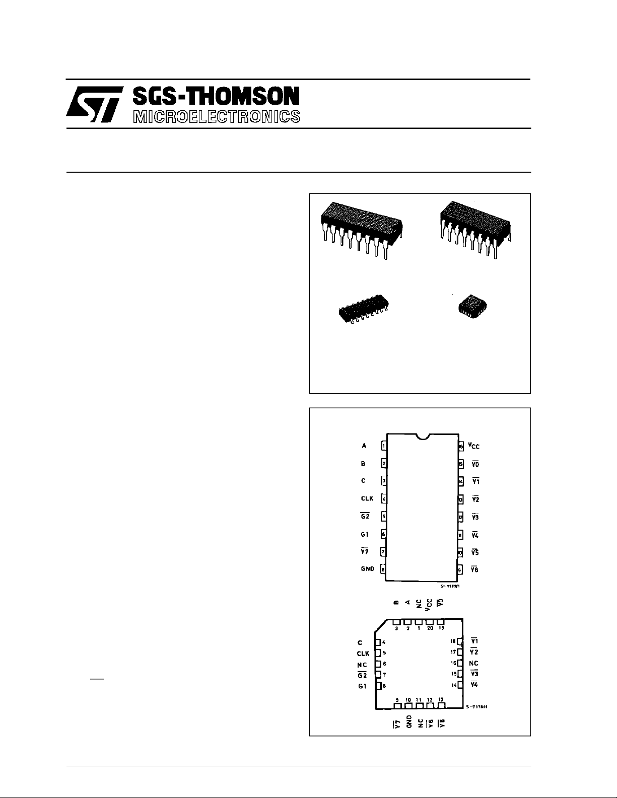
3 TO 8 LINE DECODER/LATCH
B1R
(PlasticPackage)
M1R
(MicroPackage)
ORDER CODES :
M54HC 131F1R M74H C131M1R
M74HC 131B1R M74HC1 31C1R
F1R
(CeramicPackage)
C1R
(Chip Carrier)
DESCRIPTION
The M54/74HC131 is a high speed CMOS 3 TO 8
LINE DECODER/LATCH fabricated in silicon gate
C2MOS technology.
It has the same high speed performance of LSTTL
combined withtrue CMOSlowpower consumption.
This deviceis a DECODER/LATCHcapable of selectingarbitrarilyoneof eight outputsbythreebinary
inputs A,B, and C, in thiscase, the selected output
is at logic”low”.
Also, whenENABLE input G1is setlowor ENABLE
inputG2is sethigh,selection isinhibited regardless
of otherinputsignals and all theoutputsare athigh.
All inputs are equipped with protection circuits
against static discharge and transient excess voltage.
PIN CONNECTIONS(top view)
NC =
No Internal
Connection
October 1992
1/12
Page 2
M54/M74HC131
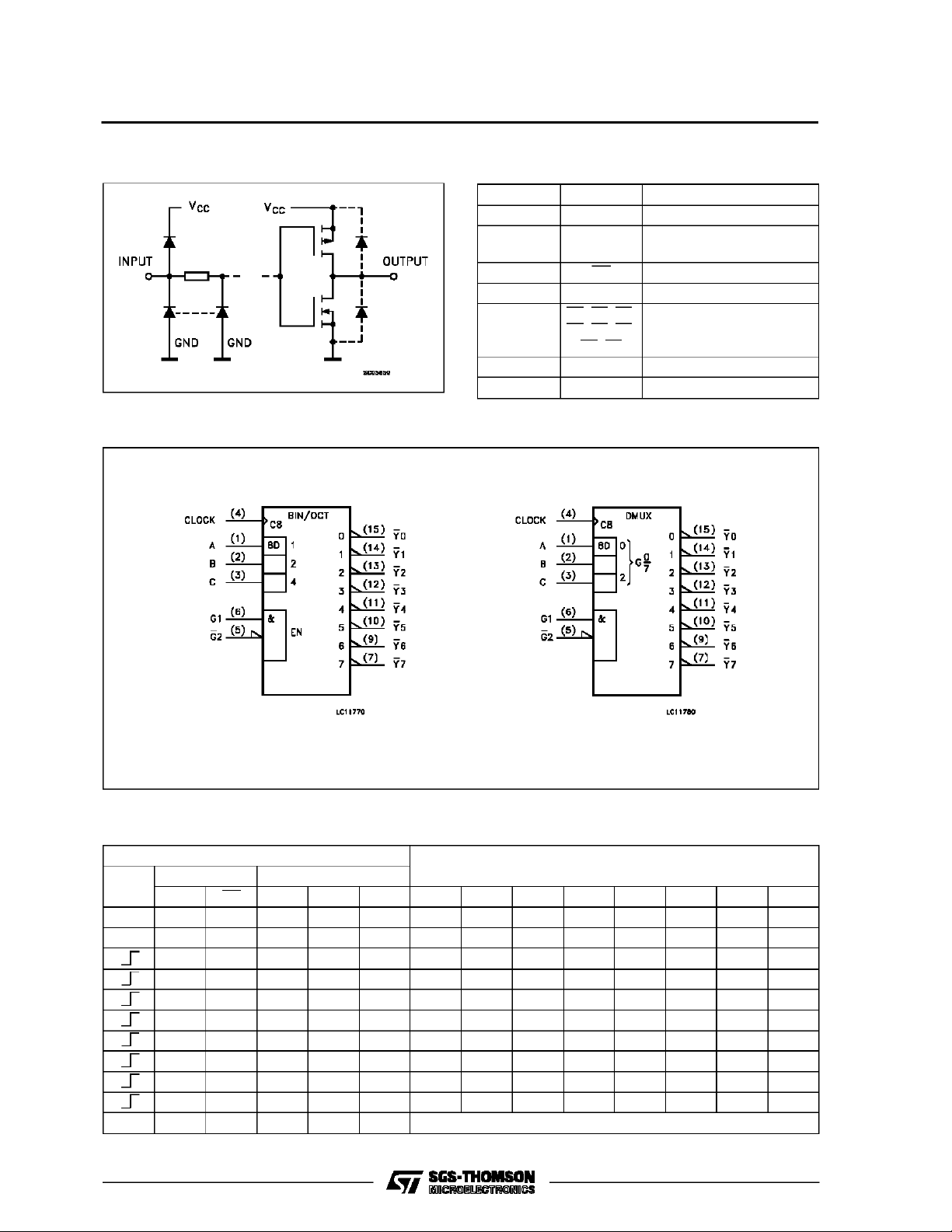
INPUT AND OUTPUT EQUIVALENT CIRCUIT
IEC LOGIC SYMBOL
PIN DESCRIPTION
PIN No SYMBOL NAME AND FUNCTION
1, 2, 3 A, B, C Data Inputs
4 CLK Clock Input (LOW to
HIGH, Edge-triggered)
5 G2 Enable (Active LOW)
6 G1 Enable (Active HIGH)
9, 10, 11,
12, 13, 14,
15, 7
8 GND Ground (0V)
16 V
Y0, Y1, Y2,
Y3, Y4, Y5,
Y6, Y7
CC
Data Outputs
Positive Supply Voltage
TRUTH TABLE
INPUTS
CLK
XXHXXXHHHHHHHH
XLXXXXHHHHHHHH
L H L X X X Outputs corresponding to stored address L: all others H
2/12
ENABLE SELECT
G1 G2 C B A Y0 Y1 Y2 Y3 Y4 Y5 Y6 Y7
HLLLLLHHHHHHH
HLLLHHLHHHHHH
HLLHLHHLHHHHH
HLLHHHHHLHHHH
HLHLLHHHHLHHH
HLHLHHHHHHLHH
HLHHLHHHHHHLH
HLHHHHHHHHHHL
OUTPUTS
Page 3
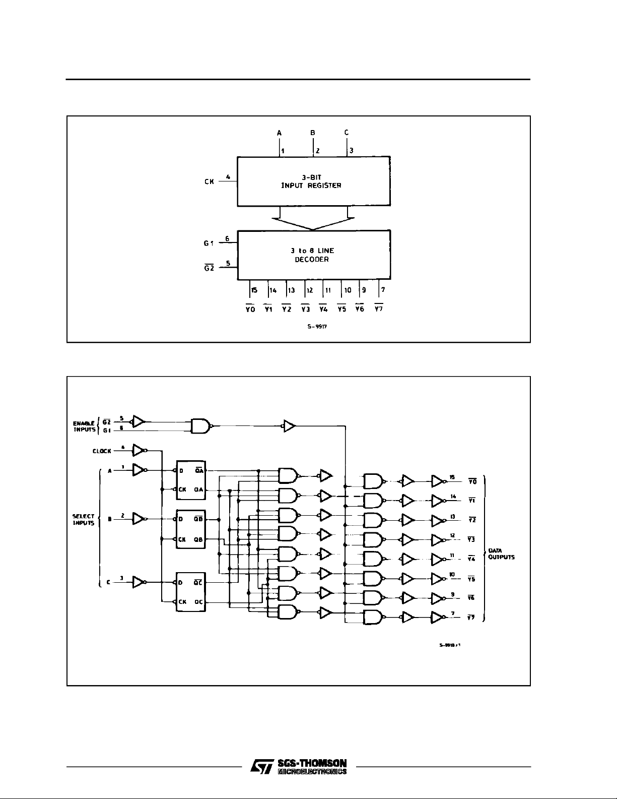
BLOCK DIAGRAM
M54/M74HC131
VCC=16
GND = 8
LOGIC DIAGRAM
3/12
Page 4
M54/M74HC131
ABSOLU TE M AXI MU M R AT INGS
Symbol Parameter Value Unit
V
CC
V
V
O
I
IK
I
OK
I
O
I
or I
CC
P
D
T
stg
T
AbsoluteMaximumRatingsarethose values beyondwhichdamage tothedevice mayoccur. Functionaloperationunder these conditionisnotimplied.
(*)500 mW: ≅ 65oC derateto300mWby 10mW/oC: 65oCto85oC
RECO MM ENDED O PERAT IN G CONDI TIONS
Symbol Parameter Value Unit
V
CC
V
I
V
O
T
op
t
r,tf
Supply Voltage -0.5 to +7 V
DC Input Voltage -0.5 to VCC+ 0.5 V
I
DC Output Voltage -0.5 to VCC+ 0.5 V
DC Input Diode Current ± 20 mA
DC Output Diode Current ± 20 mA
DC Output Source Sink Current Per Output Pin ± 25 mA
DC VCCor Ground Current ± 50 mA
GND
Power Dissipation 500 (*) mW
Storage Temperature -65 to +150
Lead Temperature (10 sec) 300
L
Supply Voltage 2 to 6 V
Input Voltage 0 to V
Output Voltage 0 to V
Operating Temperature: M54HC Series
M74HC Series
CC
CC
-55 to +125
-40 to +85
Input Rise and Fall Time VCC= 2 V 0 to 1000 ns
V
= 4.5 V 0 to 500
CC
V
= 6 V 0 to 400
CC
o
C
o
C
V
V
o
C
o
C
4/12
Page 5

DC SPECIFICATIO NS
Symbol Parameter
V
V
V
V
I
High Level Input
IH
Voltage
Low Level Input
IL
Voltage
High Level
OH
Output Voltage
Low Level Output
OL
Voltage
I
Input Leakage
I
Current
Quiescent Supply
CC
Current
M54/M74HC131
Test Conditions Value
T
=25oC
V
(V)
CC
A
54HC and 74HC
Min. Typ. Max. Min. Max. Min. Max.
2.0 1.5 1.5 1.5
4.5 3.15 3.15 3.15
6.0 4.2 4.2 4.2
2.0 0.5 0.5 0.5
4.5 1.35 1.35 1.35
6.0 1.8 1.8 1.8
2.0
4.5 4.4 4.5 4.4 4.4
6.0 5.9 6.0 5.9 5.9
4.5 I
6.0 I
2.0
4.5 0.0 0.1 0.1 0.1
6.0 0.0 0.1 0.1 0.1
4.5 I
6.0 I
6.0
=
V
I
IO=-20 µA
V
IH
or
V
IL
=-4.0 mA 4.18 4.31 4.13 4.10
O
=-5.2 mA 5.68 5.8 5.63 5.60
O
V
=
I
IO=20µA
V
IH
or
V
IL
= 4.0 mA 0.17 0.26 0.33 0.40
O
= 5.2 mA 0.18 0.26 0.33 0.40
O
VI=VCCor GND ±0.1 ±1 ±1 µA
1.9 2.0 1.9 1.9
0.0 0.1 0.1 0.1
6.0 VI=VCCor GND 4 40 80 µA
-40 to 85oC
74HC
-55 to 125oC
54HC
Unit
V
V
V
V
5/12
Page 6

M54/M74HC131
AC ELECTRICAL CHARACTERI STI CS (CL=50pF,Inputtr=tf=6ns)
Test Conditions Value
T
=25oC
Symbol Parameter
t
t
TLH
THL
Output Transition
Time
V
CC
(V)
2.0 30 75 95 110
4.5 8151922
A
54HC and 74HC
Min. Typ. Max. Min. Max. Min. Max.
6.0 7131619
t
PLH
t
PHL
Propagation
Delay Time
(CLOCK - Yn)
t
t
PLH
PHL
Propagation
Delay Time
(G - Yn)
t
W(H)
t
W(L)
Minimum Pulse
Width
(CLOCK)
Minimum Set-up
t
s
Time
2.0 78 200 250 300
4.5 26 40 50 60
6.0 22 34 43 51
2.0 60 140 175 210
4.5 15 28 35 42
6.0 13 24 30 36
2.0 20 75 95 110
4.5 6151922
6.0 6131619
2.0 25 50 65 75
4.5 5101315
6.0 5 9 11 13
t
h
Minimum Hold
Time
2.0 0 0 0
4.5 0 0 0
6.0 0 0 0
C
C
PD
Input Capacitance 5 10 10 10 pF
IN
(*) Power Dissipation
37
Capacitance
(*) CPDisdefined as the value ofthe IC’sinternal equivalent capacitance which is calculated fromthe operatingcurrent consumption without load.
(Referto Test Circuit). Average operting current canbe obtained bythe followingequation. ICC(opr) = CPD•VCC•fIN+I
-40 to 85oC
74HC
-55 to 125oC
54HC
CC
Unit
ns
ns
ns
ns
ns
ns
pF
SWITCHING CHARACTERISTICS TEST CIRCUIT
6/12
INPUT WAVEFORM
Page 7

SWITCHING CHARACTERISTICS TEST WAVEFORM
M54/M74HC131
7/12
Page 8

M54/M74HC131
Plastic DIP16 (0.25) MECHANICAL DATA
DIM.
MIN. TYP. MAX. MIN. TYP. MAX.
a1 0.51 0.020
B 0.77 1.65 0.030 0.065
b 0.5 0.020
b1 0.25 0.010
D 20 0.787
E 8.5 0.335
e 2.54 0.100
e3 17.78 0.700
F 7.1 0.280
I 5.1 0.201
L 3.3 0.130
Z 1.27 0.050
mm inch
8/12
P001C
Page 9

Ceramic DIP16/1 MECHANICAL DATA
M54/M74HC131
DIM.
MIN. TYP. MAX. MIN. TYP. MAX.
A 20 0.787
B 7 0.276
D 3.3 0.130
E 0.38 0.015
e3 17.78 0.700
F 2.29 2.79 0.090 0.110
G 0.4 0.55 0.016 0.022
H 1.17 1.52 0.046 0.060
L 0.22 0.31 0.009 0.012
M 0.51 1.27 0.020 0.050
N 10.3 0.406
P 7.8 8.05 0.307 0.317
Q 5.08 0.200
mm inch
P053D
9/12
Page 10

M54/M74HC131
SO16 (Narrow) MECHANICAL DATA
DIM.
MIN. TYP. MAX. MIN. TYP. MAX.
A 1.75 0.068
a1 0.1 0.2 0.004 0.007
a2 1.65 0.064
b 0.35 0.46 0.013 0.018
b1 0.19 0.25 0.007 0.010
C 0.5 0.019
c1 45° (typ.)
D 9.8 10 0.385 0.393
E 5.8 6.2 0.228 0.244
e 1.27 0.050
e3 8.89 0.350
F 3.8 4.0 0.149 0.157
G 4.6 5.3 0.181 0.208
L 0.5 1.27 0.019 0.050
M 0.62 0.024
S8°(max.)
mm inch
10/12
P013H
Page 11

PLCC20 MECHANICAL DATA
M54/M74HC131
DIM.
MIN. TYP. MAX. MIN. TYP. MAX.
A 9.78 10.03 0.385 0.395
B 8.89 9.04 0.350 0.356
D 4.2 4.57 0.165 0.180
d1 2.54 0.100
d2 0.56 0.022
E 7.37 8.38 0.290 0.330
e 1.27 0.050
e3 5.08 0.200
F 0.38 0.015
G 0.101 0.004
M 1.27 0.050
M1 1.14 0.045
mm inch
P027A
11/12
Page 12

M54/M74HC131
Information furnishedis believed to be accurate and reliable. However, SGS-THOMSON Microelectronicsassumes no responsability for the
consequences of useof suchinformation nor for any infringement of patents or other rights of third parties which may results from its use. No
license is granted byimplication or otherwiseunder any patentor patentrights ofSGS-THOMSON Microelectronics.Specificationsmentioned
in this publication are subjectto changewithout notice. This publication supersedes andreplaces all information previouslysupplied.
SGS-THOMSON Microelectronicsproducts are not authorized foruse ascritical componentsinlifesupportdevices orsystemswithoutexpress
written approval of SGS-THOMSON Microelectonics.
1994SGS-THOMSON Microelectronics- All Rights Reserved
Australia -Brazil - France - Germany - Hong Kong - Italy - Japan - Korea - Malaysia - Malta -Morocco - The Netherlands-
Singapore -Spain - Sweden- Switzerland - Taiwan - Thailand- UnitedKingdom - U.S.A
SGS-THOMSON Microelectronics GROUP OFCOMPANIES
12/12
 Loading...