

Datasheet M74HC07TTR, M74HC07RM13TR, M74HC07M1R, M74HC07B1R Datasheet (SGS Thomson Microelectronics)
Page 1
■ HIGH SPEED:
t
= 6ns (TYP.) at VCC=6V
PD
■ LOW POWER DISSIPATION:
=1µA(MAX.) at TA=25°C
I
CC
■ HIGH NOISE IMMUNITY:
V
NIH=VNIL
■ WIDE OPERATING VOLTAGE RANGE:
V
(OPR) = 2V to 6V
CC
■ PIN AND FUNCTION COMPATIBLE WITH
=28%VCC(MIN.)
74 SERIES 07
DESCRIPTION
The M74HC07 is an high speed CMOS HEX
OPEN DRAIN BUFFER fabricated with silicon
gate C
2
MOS technology.
The internal circuit is composed of 2 stages
including buffer output, which enables high noise
immunity and stable output.
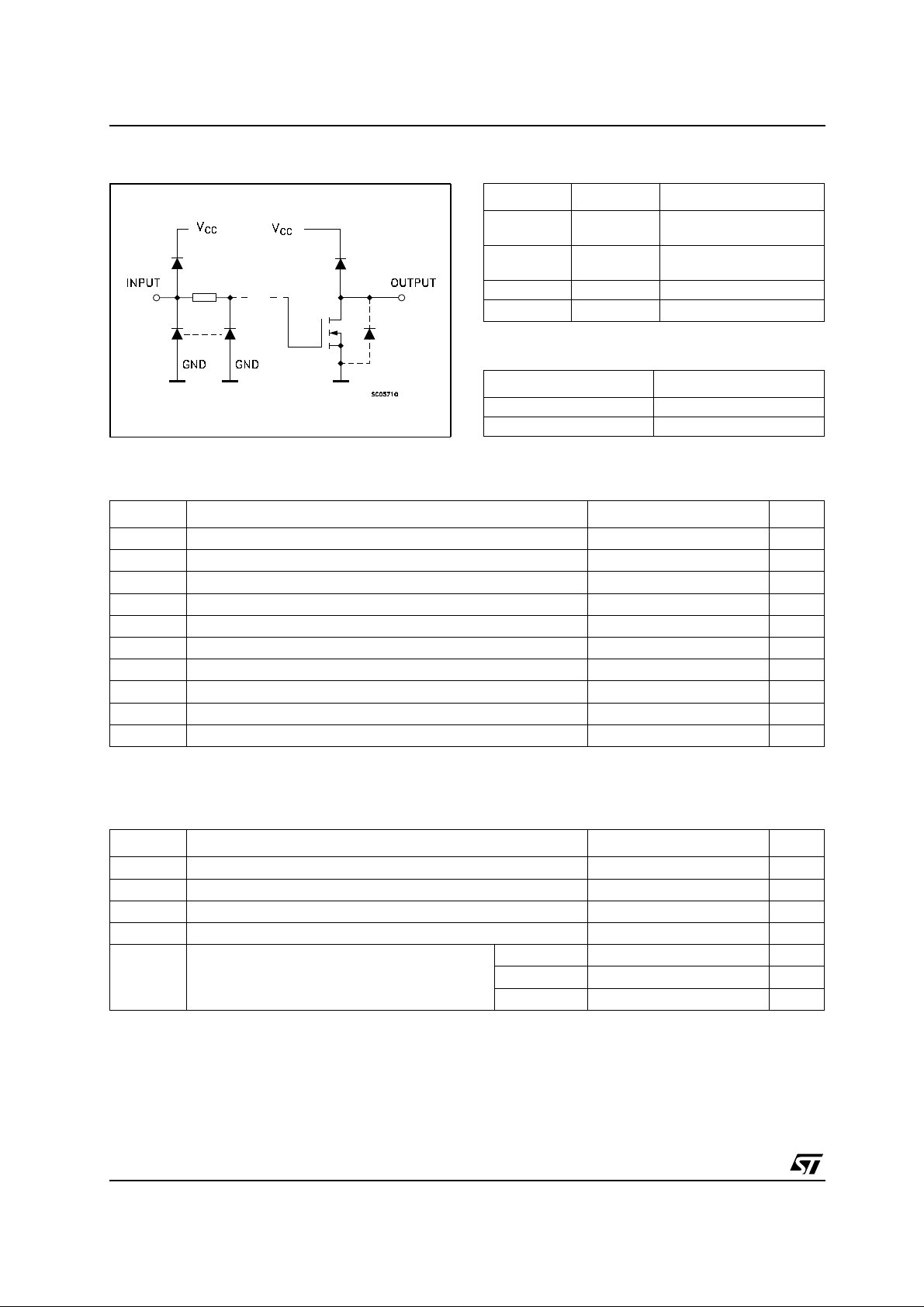
M74HC07
HEX BUFFER (OPEN DRAIN)
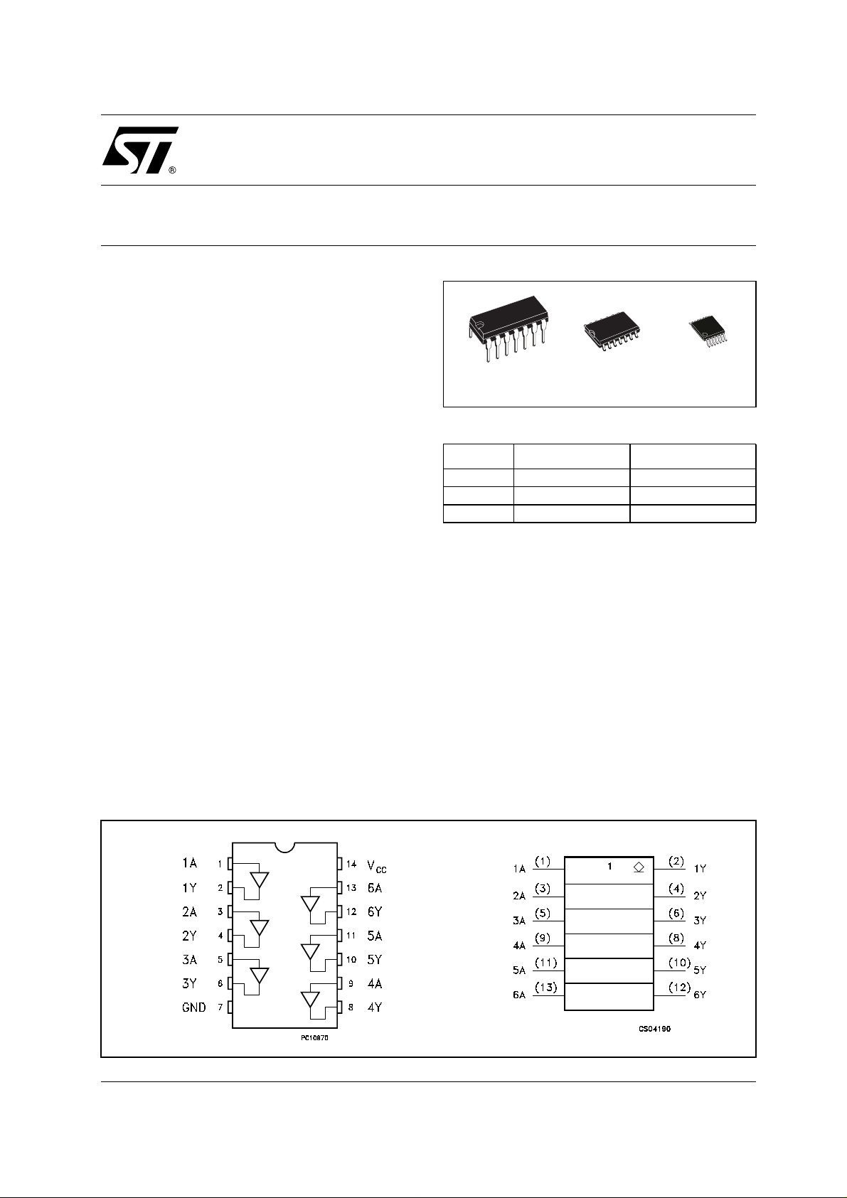
TSSOPDIP SOP
ORDER CODES
PACKAGE TUBE T & R
DIP M74HC07B1R
SOP M74HC07M1R M74HC07RM13TR
TSSOP M74HC07TTR
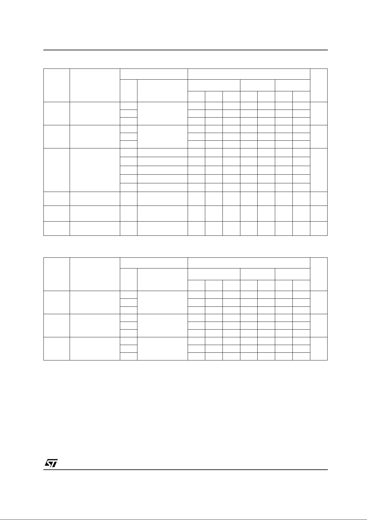
All inputs are equipped with protection circuits
against static discharge and transient excess
voltage.
PIN CONNECTION AND IEC LOGIC SYMBOLS
1/10May 2003
Page 2
M74HC07
INPUT AND OUTPUT EQUIVALENT CIRCUIT PIN DESCRIPTION
PIN No SYMBOL NAME AND FUNCTION
1, 3, 5, 9, 11,
13
2, 4, 6, 8, 10,
12
7 GND Ground (0V)
14
TRUTH TABLE
Z : High Impedance
ABSOLUTE MAXIMUM RATINGS
Symbol Parameter Value Unit
V
V
V
I
I
OK
I
or I
I
CC
P
T
T
Absolute Maximum Ratings are those values beyond which damage to the device may occur. Functional operation under these conditions is
not implied
(*) 500mW at 65
Supply Voltage
CC
DC Input Voltage -0.5 to VCC+ 0.5
I
DC Output Voltage -0.5 to VCC+ 0.5
O
DC Input Diode Current
IK
DC Output Diode Current
DC Output Current
O
DC VCCor Ground Current
GND
Power Dissipation
D
Storage Temperature
stg
Lead Temperature (10 sec)
L
°C; derate to 300mW by 10mW/°Cfrom65°Cto85°C
1A to 6A Data Inputs
1Y to 6Y Data Outputs
V
CC
Positive Supply Voltage
AY
LL
HZ
-0.5 to +7 V
V
V
± 20 mA
± 20 mA
± 25 mA
± 50 mA
500(*) mW
-65 to +150 °C
300 °C
RECOMMENDED OPERATING CONDITIONS
Symbol Parameter Value Unit
Supply Voltage
CC
Input Voltage 0 to V
I
Output Voltage 0 to V
O
Operating Temperature
op
Input Rise and Fall Time VCC= 2.0V
V
= 4.5V
CC
= 6.0V
V
CC
2to6 V
CC
CC
-55 to 125 °C
0 to 1000 ns
0 to 500 ns
0 to 400 ns
2/10
V
V
T
t
V
r,tf
V
V
Page 3
DC SPECIFICATIONS
Symbol Parameter
V
V
High Level Input
IH
Voltage
V
Low Level Input
IL
Voltage
Low Level Output
OL
Voltage
Input Leakage
I
I
Current
I
Output Leakage
OZ
Current
I
Quiescent Supply
CC
Current
M74HC07
Test Condition Value
= 25°C
T
V
CC
(V)
A
Min. Typ. Max. Min. Max. Min. Max.
2.0 1.5 1.5 1.5
6.0 4.2 4.2 4.2
2.0 0.5 0.5 0.5
6.0 1.8 1.8 1.8
2.0
4.5
6.0
4.5
6.0
6.0
6.0
6.0
IO=20 µA
=20 µA
I
O
=20 µA
I
O
=4.0 mA
I
O
=5.2 mA
I
O
V
I=VCC
VI=VIHor V
or GND
IL
VO=VCCor GND
V
I=VCC
or GND
0.0 0.1 0.1 0.1
0.0 0.1 0.1 0.1
0.0 0.1 0.1 0.1
0.17 0.26 0.33 0.40
0.18 0.26 0.33 0.40
-40 to 85°C -55 to 125°C
± 0.1 ± 1 ± 1 µA
±0.5 ± 5 ± 10 µA
11020µA
Unit
V4.5 3.15 3.15 3.15
V4.5 1.35 1.35 1.35
V
AC ELECTRICAL CHARACTERISTICS (C
Test Condition Value
Symbol Parameter
t
t
t
Output Transition
THL
Time
Propagation Delay
PLZ
Time
Propagation Delay
PZL
Time
V
CC
(V)
2.0 30 75 95 110
6.0 7 13 16 19
2.0
R
L
6.0 6 15 20 23
2.0
R
L
6.0 5 15 20 23
= 50 pF, Input tr=tf=6ns)
L
= 25°C
T
A
Min. Typ. Max. Min. Max. Min. Max.
10 90 115 135
=1KΩ
17 90 115 135
=1KΩ
-40 to 85°C -55 to 125°C
Unit
ns4.5 8 15 19 22
ns4.5 7 18 23 27
ns4.5 7 18 23 27
3/10
Page 4

M74HC07
CAPACITIVE CHARACTERISTICS
Test Condition Value
= 25°C
Symbol Parameter
V
CC
(V)
C
C
C
1) CPDis defined as the value of the IC’s internal equivalent capacitance which is calculated from the operating current consumption without
load. (Refer to Test Circuit). Average operating current can be obtained by the following equation. I
Input Capacitance
IN
Output
OUT
Capacitance
Power Dissipation
PD
Capacitance (note1)5.0 4 pF
5.0 5 10 10 10 pF
5.0 3 pF
T
A
Min. Typ. Max. Min. Max. Min. Max.
TEST CIRCUIT
-40 to 85°C -55 to 125°C
CC(opr)=CPDxVCCxfIN+ICC
Unit
/6 (per gate)
CL= 50pF or equivalent (includes jig and probe capacitance)
R
T=ZOUT
of pulse generator (typically 50Ω)
WAVEFORM : PROPAGATION DELAY T IME (f=1MHz; 50% duty cycle)
4/10
Page 5

M74HC07
Plastic DIP-14 MECHANICAL DATA
mm. inch
DIM.
MIN. TYP MAX. MIN. TYP. MAX.
a1 0.51 0.020
B 1.39 1.65 0.055 0.065
b 0.5 0.020
b1 0.25 0.010
D 20 0.787
E 8.5 0.335
e 2.54 0.100
e3 15.24 0.600
F 7.1 0.280
I 5.1 0.201
L 3.3 0.130
Z 1.27 2.54 0.050 0.100
P001A
5/10
Page 6

M74HC07
SO-14 MECHANICAL DATA
DIM.
A 1.75 0.068
a1 0.1 0.2 0.003 0.007
a2 1.65 0.064
b 0.35 0.46 0.013 0.018
b1 0.19 0.25 0.007 0.010
C 0.5 0.019
c1 45˚ (typ.)
D 8.55 8.75 0.336 0. 344
E 5.8 6.2 0.228 0.244
e 1.27 0.050
e3 7.62 0.300
F 3.8 4.0 0.149 0.157
G 4.6 5.3 0.181 0.208
L 0.5 1.27 0.019 0.050
M 0.68 0.026
S ˚ (max.)
MIN. TYP MAX. MIN. TYP. MAX.
mm. inch
8
6/10
PO13G
Page 7

M74HC07
TSSOP14 MECHANICAL DATA
mm. inch
DIM.
MIN. TYP MAX. MIN. TYP. MAX.
A 1.2 0.047
A1 0.05 0.15 0.002 0.004 0.006
A2 0.8 1 1.05 0.031 0.039 0.041
b 0.19 0.30 0.007 0.012
c 0.09 0.20 0.004 0.0089
D 4.9 5 5.1 0.193 0.197 0.201
E 6.2 6.4 6.6 0.244 0.252 0.260
E1 4.3 4.4 4.48 0.169 0.173 0.176
e 0.65 BSC 0.0256 BSC
K0˚ 8˚0˚ 8˚
L 0.45 0.60 0.75 0.018 0.024 0.030
A2
A
A1
b
e
c
K
L
E
D
E1
PIN 1 IDENTIFICATION
1
0080337D
7/10
Page 8

M74HC07
Tape & Reel SO-14 MECHANICAL DATA
mm. inch
DIM.
MIN. TYP MAX. MIN. TYP. MAX.
A 330 12.992
C 12.8 13.2 0.504 0.519
D 20.2 0.795
N 60 2.362
T 22.4 0.882
Ao 6.4 6.6 0.252 0.260
Bo 9 9.2 0.354 0.362
Ko 2.1 2.3 0.082 0.090
Po 3.9 4.1 0.153 0.161
P 7.9 8.1 0.311 0.319
8/10
Page 9

M74HC07
Tape & Reel TSSOP14 MECHANICAL DATA
mm. inch
DIM.
MIN. TYP MAX. MIN. TYP. MAX.
A 330 12.992
C 12.8 13.2 0.504 0.519
D 20.2 0.795
N 60 2.362
T 22.4 0.882
Ao 6.7 6.9 0.264 0.272
Bo 5.3 5.5 0.209 0.217
Ko 1.6 1.8 0.063 0.071
Po 3.9 4.1 0.153 0.161
P 7.9 8.1 0.311 0.319
9/10
Page 10

M74HC07
Information furnished is believed to be accurate and reliable. However, STMicroelectronics assumes no responsibility for the
consequences of use o f suc h inf ormat ion n or f or an y infr ingeme nt of paten ts or oth er ri gh ts of third part ies whic h may resul t f rom
its use. No license is granted by implication or otherwise under any patent or patent rights of STMicroelectronics. Specifications
mentioned in this publication are subject to change without notice. This publication supersedes and replaces all information
previously supplied. STMicroelectronics products are not authorized for use as critical components in life support devices or
systems without express written approval of STMicroelectronics.
Australia - Brazil - Canada - China - Finland - France - Germany - Hong Kong - India - Israel - Italy - Japan - Malaysia - Malta - Morocco
© The ST logo is a registered trademark of STMicroelectronics
© 2003 STMicroelectronics - Printed in Italy - All Rights Reserved
STMicroelectronics GROUP OF COMPANIES
Singapore - Spain - Sweden - Switzerland - United Kingdom - United States.
© http://www.st.com
10/10
 Loading...