

Page 1
.HIGH SPEED
tPD= 8 ns (TYP.)AT VCC=5V
.LOWPOWER DISSIPATION
ICC=1 µA (MAX.) AT TA=25°C
.HIGH NOISE IMMUNITY
V
NIH=VNIL
=28%VCC(MIN.)
.OUTPUT DRIVE CAPABILITY
10 LSTTLLOADS
.WIDE OPERATING VOLTAGERANGE
VCC(OPR)= 2 V TO6 V
.PIN AND FUNCTION COMPATIBLE WITH
54/74LS05
M54HC05
M74HC05
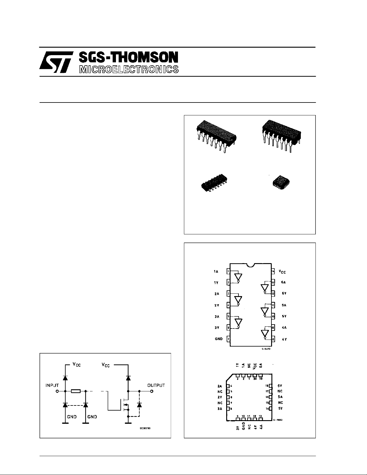
HEX INVERTER (OPEN DRAIN)
B1R
(PlasticPackage)
M1R
(MicroPackage)
ORDER CODES :
M54HC 05F1R M74H C05M1R
M74HC 05B1R M74HC0 5C1R
F1R
(CeramicPackage)
C1R
(Chip Carrier)
DESCRIPTION
The M54/74HC05 is a high speed CMOS HEX
OPEN DRAININVERTER fabricated in silicongate
C2MOStechnology.It hasthesamehighspeedperformance of LSTTL combined with true CMOS low
powerconsumption.
The internal circuitis composedof 3stages including buffer output, which enables high noise immunity and stable output. All inputs are equipped
with circuits against static discharge and transient
excess voltage.
INPUT AND OUTPUT EQUIVALENT CIRCUIT
PIN CONNECTIONS (top view)
NC =
No Internal
Connection
February 1993
1/9
Page 2
M54/M74HC05
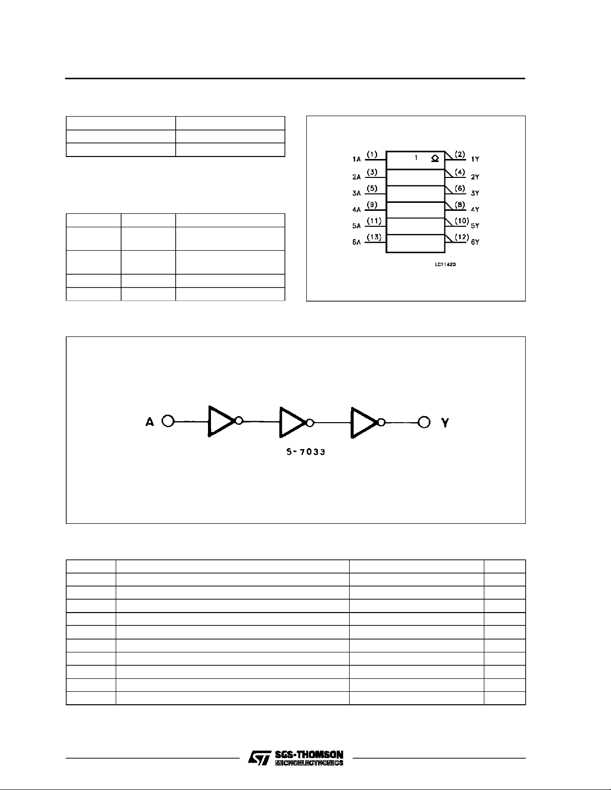
TRUTH TABLE
AY
LZ
HL
Z =High impedance
PIN DESCRIPTION
PIN No SYMBOL NAME AND FUNCTION
1, 3, 5, 9,
1A to 6A Data Inputs
11, 13
2, 4, 6, 8,
1Y to 6Y Data Outputs
10, 12
7 GND Ground (0V)
14 V
CC
Positive Supply Voltage
LOGI C DIAG RAM (Pe r G at e )
IEC LOGIC SYMBOL
ABSOLU TE MAXIMU M RATINGS
Symbol Parameter Value Unit
V
CC
V
V
O
I
IK
I
OK
I
O
or I
I
CC
P
D
T
stg
T
L
AbsoluteMaximumRatingsarethosevalues beyond whichdamagetothedevicemayoccur.Functional operation under theseconditionisnotimplied.
(*)500 mW:≅ 65oC derateto300mWby 10mW/oC: 65oCto85oC
2/9
Supply Voltage -0.5 to +7 V
DC Input Voltage -0.5 to VCC+ 0.5 V
I
DC Output Voltage -0.5 to VCC+ 0.5 V
DC Input Diode Current ± 20 mA
DC Output Diode Current ± 20 mA
DC Output Sink Current Per Output Pin 25 mA
DC VCCor Ground Current ± 50 mA
GND
Power Dissipation 500 (*) mW
Storage Temperature -65 to +150
Lead Temperature (10 sec) 300
o
C
o
C
Page 3
M54/M74HC05
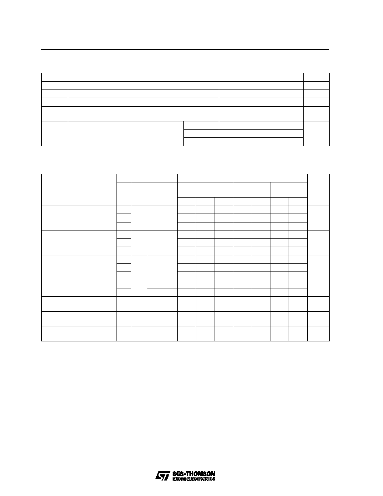
RECO MM ENDED O PERAT IN G C ONDITIO NS
Symbol Parameter Value Unit
V
V
V
T
t
r,tf
DC SPECIFICA TIONS
Symbol Parameter
V
IH
V
V
OL
I
I
OZ
I
CC
Supply Voltage 2 to 6 V
CC
Input Voltage 0 to V
I
Output Voltage 0 to V
O
Operating Temperature: M54HC Series
op
M74HC Series
CC
CC
-55 to +125
-40 to +85
Input Rise and Fall Time VCC= 2 V 0 to 1000 ns
V
= 4.5 V 0 to 500
CC
V
= 6 V 0 to 400
CC
Test Conditions Value
V
(V)
CC
=25oC
T
A
54HC and 74HC
-40 to 85oC
74HC
-55 to 125oC
Min. Typ. Max. Min. Max. Min. Max.
High Level Input
Voltage
2.0 1.5 1.5 1.5
4.5 3.15 3.15 3.15
6.0 4.2 4.2 4.2
Low Level Input
IL
Voltage
2.0 0.5 0.5 0.5
4.5 1.35 1.35 1.35
6.0 1.8 1.8 1.8
Low Level Output
Voltage
Input Leakage
I
Current
Output Leakage
Current
Quiescent Supply
2.0
V
=
I
4.5 0.0 0.1 0.1 0.1
6.0 0.0 0.1 0.1 0.1
4.5 I
6.0 I
6.0
6.0
IO=20µA
V
IH
or
V
IL
= 4.0 mA 0.17 0.26 0.33 0.40
O
= 5.2 mA 0.18 0.26 0.33 0.40
O
VI=VCCor GND ±0.1 ±1 ±1 µA
VI=VIHor V
IL
VO=VCCor GND
0.0 0.1 0.1 0.1
±0.5 ±5 ±10 µA
6.0 VI=VCCor GND 1 10 20 µA
Current
54HC
V
V
o
C
o
C
Unit
V
V
V
3/9
Page 4

M54/M74HC05
AC ELECTRICAL CHARACTERISTICS (CL=50pF,Inputtr=tf=6ns)
Test Conditions Value
T
=25oC
Symbol Parameter
t
THL
Output Transition
Time
V
CC
(V)
2.0 30 75 95 110
4.5 8151922
A
54HC and 74HC
Min. Typ. Max. Min. Max. Min. Max.
6.0 7131619
t
PLZ
Propagation
Delay Time
2.0 RL=1KΩ 20 90 115 135
4.5 11 18 23 27
6.0 10 15 20 23
t
PZL
Propagation
Delay Time
2.0 RL=1KΩ 33 90 115 135
4.5 9182327
6.0 8152023
C
C
Input Capacitance 5 10 10 10 pF
IN
OUT
Output
10
Capacitance
C
(*) Power Dissipation
PD
6.5
Capacitance
(*) CPDisdefined as the valueofthe IC’s internal equivalentcapacitance which is calculated from the operatingcurrentconsumption without load.
-40 to 85oC
74HC
-55 to 125oC
54HC
Unit
ns
ns
ns
pF
pF
4/9
Page 5

Plastic DIP14 MECHANICAL DATA
M54/M74HC05
DIM.
MIN. TYP. MAX. MIN. TYP. MAX.
a1 0.51 0.020
B 1.39 1.65 0.055 0.065
b 0.5 0.020
b1 0.25 0.010
D 20 0.787
E 8.5 0.335
e 2.54 0.100
e3 15.24 0.600
F 7.1 0.280
I 5.1 0.201
L 3.3 0.130
Z 1.27 2.54 0.050 0.100
mm inch
P001A
5/9
Page 6

M54/M74HC05
Ceramic DIP14/1 MECHANICAL DATA
DIM.
MIN. TYP. MAX. MIN. TYP. MAX.
A 20 0.787
B 7.0 0.276
D 3.3 0.130
E 0.38 0.015
e3 15.24 0.600
F 2.29 2.79 0.090 0.110
G 0.4 0.55 0.016 0.022
H 1.17 1.52 0.046 0.060
L 0.22 0.31 0.009 0.012
M 1.52 2.54 0.060 0.100
N 10.3 0.406
P 7.8 8.05 0.307 0.317
Q 5.08 0.200
mm inch
6/9
P053C
Page 7

SO14 MECHANICAL DATA
M54/M74HC05
DIM.
MIN. TYP. MAX. MIN. TYP. MAX.
A 1.75 0.068
a1 0.1 0.2 0.003 0.007
a2 1.65 0.064
b 0.35 0.46 0.013 0.018
b1 0.19 0.25 0.007 0.010
C 0.5 0.019
c1 45° (typ.)
D 8.55 8.75 0.336 0.344
E 5.8 6.2 0.228 0.244
e 1.27 0.050
e3 7.62 0.300
F 3.8 4.0 0.149 0.157
G 4.6 5.3 0.181 0.208
L 0.5 1.27 0.019 0.050
M 0.68 0.026
S8°(max.)
mm inch
P013G
7/9
Page 8

M54/M74HC05
PLCC20 MECHANICAL DATA
DIM.
MIN. TYP. MAX. MIN. TYP. MAX.
A 9.78 10.03 0.385 0.395
B 8.89 9.04 0.350 0.356
D 4.2 4.57 0.165 0.180
d1 2.54 0.100
d2 0.56 0.022
E 7.37 8.38 0.290 0.330
e 1.27 0.050
e3 5.08 0.200
F 0.38 0.015
G 0.101 0.004
M 1.27 0.050
M1 1.14 0.045
mm inch
8/9
P027A
Page 9

M54/M74HC05
Information furnished is believed to be accurate and reliable. However, SGS-THOMSON Microelectronics assumes no responsability for the
consequences of use of such information nor for any infringement of patents or other rights of third parties which may results from its use. No
license is granted byimplication or otherwise under any patent or patentrights of SGS-THOMSON Microelectronics. Specificationsmentioned
in this publication are subject to change without notice. This publication supersedes and replaces all information previously supplied.
SGS-THOMSON Microelectronicsproductsarenotauthorizedforuse ascriticalcomponentsinlifesupportdevicesorsystemswithoutexpress
written approval of SGS-THOMSON Microelectonics.
1994 SGS-THOMSON Microelectronics - All Rights Reserved
Australia - Brazil - France - Germany - Hong Kong - Italy - Japan - Korea - Malaysia - Malta - Morocco - The Netherlands -
Singapore -Spain - Sweden- Switzerland -Taiwan - Thailand - UnitedKingdom - U.S.A
SGS-THOMSON Microelectronics GROUP OF COMPANIES
9/9
 Loading...