

Page 1
64K x 72-bit Entry NETWORK PACKET SEARCH ENGINE
FEATURES SUMMARY
■ 64K DATA ENT RIES IN 72-B IT MODE
■ TABLE MAY BE PARTITIONED INTO UP TO
EIGHT(8) OCTANTS
(Data entry width in each octant is configurab le
as 36, 72, 144, or 288 bits.)
■ UP TO 100MILLIONSUSTAINED SEA RCHE S
PER SE COND IN 72-B I T and 144-B IT
CONFIGURATIONS
■ UP TO 50 MILLION SEARCHES PER
SECOND IN 36-BIT and 288-BIT
CONFIGURATIONS
■ SEARCHES ANY SUB-FIELD IN A SINGLE
CYCLE
■ OFFERS BIT-BY-BIT and GLOBAL MASKING
■ SYNCHRONOUS, PIPELINED OPERATION
■ UP TO 31 SEARCH ENGINES CA SCADAB LE
WITHOUT PERFORMANCE DEGRADATION
■ WHEN CASCADED, THE DATABASE
ENTRIES CAN SCAL E F ROM 496K TO 3968K
DEPENDING O N THE WIDTH OF THE ENTRY
■ GLUELESS INTERFACE TO INDUSTRY-
STANDARD SRAMS
■ SIMPLE HARDWARE INSTRUCTION
INTERFACE
■ IEEE 1149.1 TEST ACCESS PORT
■ OPERATING SUPPLY VOLTAGES INCLUDE:
(Operating Core Supply Voltage) = 1.5V for
V
DD
66 and 83MSPS; 1.65V for 100MSPS
(Operating Supply Voltage for I/O) = 2.5
V
DDQ
or 3.3V
■ 388 PBGA, 35mm x 35mm
M7040N
PRELIMINARY DATA
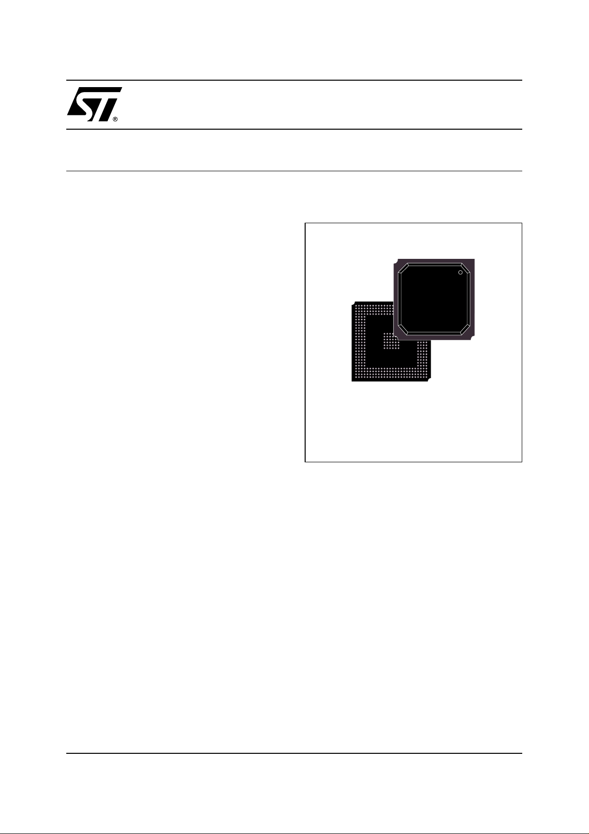
Figure 1. 388-ball PBGA Package
388-ball PBGA
35mm x 35mm
May 2002
1/159
Page 2

M7040N
TABLE OF CONTENTS
DESCRIPTION ....................................................................7
Overview......................................................................7
Performance...................................................................7
Applications....................................................................7
Product Range (Table 1.) . ........................................................7
Switch/Router Implementation Using the M7040N (Figure 2.) .............................7
SignalNames(Table2.)..........................................................8
Connections (Figure 3.). . . ........................................................9
M7040NBlockDiagram(Figure4.).................................................10
MAXIMUMRATING................................................................11
AbsoluteMaximumRatings(Table3.) ..............................................11
DC AND AC PARAMETERS . . .......................................................12
DC and AC Measurement Conditions (Table 4.). . . ....................................12
M7040N 1.8, 2.5, or 3.3V A C Testing Load (Figure 5.) ..................................13
M7040N 1.8, 2.5, or 3.3V Input Waveform (Figure 6.) ..................................13
M7040N1.8,2.5,or3.3VI/OOutputLoadEquivalent(Figure7.) .........................13
Capacitance (Table 5.) . . . .......................................................14
DCCharacteristics(Table6.).....................................................14
ACTimingWaveformswithCLK2X(Figure8.)........................................15
ACTimingWaveformswithCLK1X(Figure9.)........................................16
ACTimingParameterswithCLK2X(Table7.)........................................17
ACTimingParameterswithCLK1X(Table8.)........................................18
OPERATION.....................................................................19
CommandBusandDQBus ......................................................19
DatabaseEntry(DataArrayandMaskArray).........................................19
Arbitration Logic. . . .............................................................19
PipelineandSRAMControl.......................................................19
FullLogic.....................................................................19
Connection Descriptions . . .......................................................19
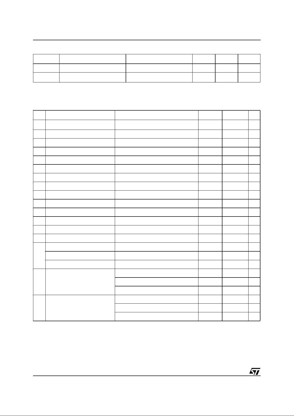
CLOCKS........................................................................21
Clocks(CLK2XandPHS_L)(Figure10.)............................................21
Clocks(CLK1X)(Figure11.)......................................................21
ClocksforAllTimingDiagrams(Figure12.)..........................................22
PLLUSAGE .....................................................................22
2/159
Page 3

M7040N
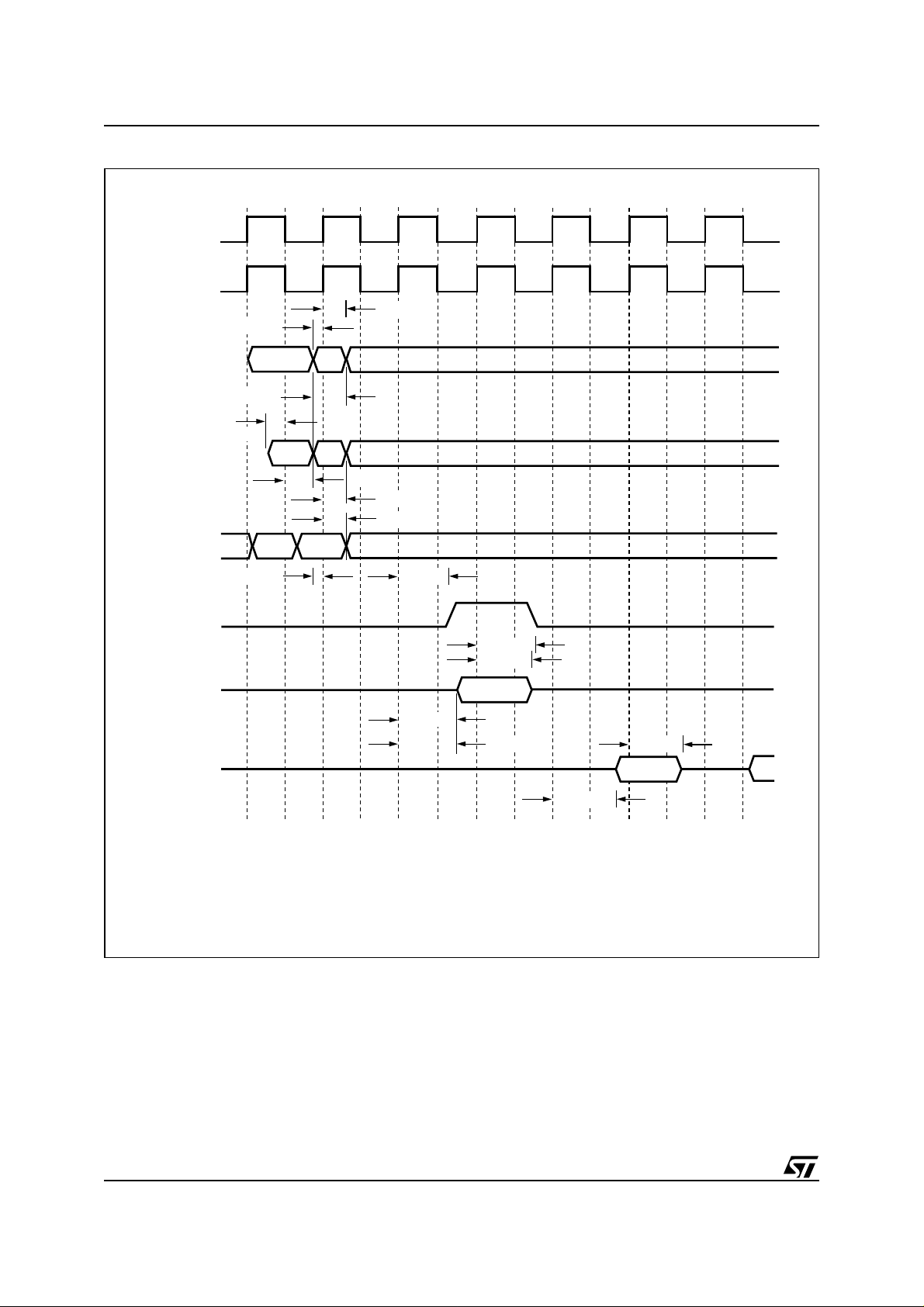
REGISTERS.....................................................................22
RegisterOverview(Table9.)......................................................22
ComparandRegisters...........................................................23
ComparandRegisterSelectionDuringSEARCHandLEARNInstructions(Figure13.).........23
MaskRegisters................................................................23
AddressingtheGlobalMasksRegisterArray(Figure14.) ...............................23
SEARCH-Successful Registers (SSR[0:7]). ..........................................24
SEARCH-Successful Register (S S R ) Description (Table 10.).............................24
TheCommandRegister .........................................................25
CommandRegisterFieldDescriptions(Table11.).....................................25
TheInformationRegister.........................................................26
InformationRegisterFieldDescriptions(Table12.) ....................................26
TheReadBurstAddressRegister(RBURREG).......................................27
ReadBurstRegisterDescription(Table13.)..........................................27
The Write Burst Address Register (WBURREG). . . ....................................27
WriteBurstRegisterDescription(Table14.)..........................................27
TheNFARegister..............................................................27
NFARegister(Table15.).........................................................27
SEARCH ENGINE ARCHITECTURE . .................................................28
DataandMaskAddressing.......................................................28
M7040NDatabaseWidthConfiguration(Figure15.) ...................................28
BitPositionMatch(Table16.).....................................................29
Multi-widthConfigurationExample(Figure16.) .......................................29
M7040NDataandMaskArrayAddressing(Figure17.).................................29
COMMAND CODES AND PARAMETERS ..............................................30
CommandCodes...............................................................30
CommandsandCommandParameters.............................................30
CommandCodes(Table17.) .....................................................30
CommandParameters(Table18.).................................................31
READCOMMAND.................................................................32
SingleLocationREADCycleTiming(Figure18.)......................................33
BurstREADoftheDataandMaskArrays(BLEN=4)(Figure19.)........................33
READCommandParameters(Table19.)............................................34
DataandMaskArray,SRAMReadAddressFormat(Table20.)..........................34
READAddressFormatforInternalRegisters(Table21.)................................35
READAddressFormatforDataandMaskArrays(Table22.)............................35
3/159
Page 4

M7040N
WRITECOMMAND................................................................35
SingleLocationWRITECycleTiming(Figure20.) .....................................36
BurstWRITEoftheDataandMaskArrays(BLEN=4)(Figure21.)........................37
(Single)WRITEAddressFormatforDataandMaskArraysorSRAM(Table23.).............37
WRITEAddressFormatforInternalRegisters(Table24.)...............................38
WRITEAddressFormatforDataandMaskArray(BurstWrite)(Table25.)..................38
ParallelWRITE................................................................38
SEARCH COMMAND . .............................................................38
72-bitConfigurationwithSingleDevice...........................................38
HardwareDiagramforaTablewithOneDevice(Figure22.).............................39
72-BitConfigurationSEARCHTimingDiagramforOneDevice(Figure23.).................40
x72TablewithOneDevice(Figure24.).............................................41
LatencyofSEARCHfromInstructiontoSRAMAccessCycle,72-bit(Table26.)..............41
ShiftofSSFandSSVfromSADR(Table27.).........................................41
72-bit SEARCH on Tables Configured as x72 Using up to Eight M 7040N Devices.........42
Hit/MissAssumption(Table28.)...................................................43
HardwareDiagramforaTablewithEightDevices(Figure25.) ...........................43
x72TablewithEightDevices(Figure26.)............................................44
Timing Diagrams for x72 Using up to Eight M7040N Devices.............................45
LatencyofSEARCHfromInstructiontoSRAMAccessCycle(Table29.)...................48
ShiftofSSFandSSVfromSADR(Table30.).........................................48
72-bit Search on Tables Configured as x72 Using Up To 31 M7040N Devices . . ..........48
Hit/MissAssumption(Table31.)...................................................49
HardwareDiagramforaTablewith31Devices(Figure30.) .............................50
HardwareDiagramforaBlockofUpToEightDevices(Figure31.)........................51
x72Tablewith31Devices(Figure32.)..............................................52
TimingDiagramsforx72UsingUpTo31M7040NDevices..............................53
LatencyofSEARCHfromInstructiontoSRAMAccessCycle(Table32.)...................64
ShiftofSSFandSSVfromSADR(Table33.).........................................64
144-bitConfigurationwithSingleDevice..........................................64
HardwareDiagramforaTablewith1Device(Figure44.) ...............................65
Timing Diag ram for a 144-bit SEARCH for 1 Device (Figure 45.) . . . .......................66
x144TablewithOneDevice(Figure46.)............................................67
LatencyofSEARCHfromInstructiontoSRAMAccessCycle,144-bit(Table34.).............67
ShiftofSSFandSSVfromSADR(Table35.).........................................67
144-bitSearchonTablesConfiguredasx144UsingUptoEightM7040NDevices........68
Hit/MissAssumption(Table36.)...................................................69
HardwareDiagramforaTablewithEightDevices(Figure47.) ...........................69
x144TablewithEightDevices(Figure48.)...........................................70
TimingDiagramsforx144UsingUptoEightM7040NDevices...........................71
LatencyofSEARCHfromInstructiontoSRAMAccessCycle,144-bit(Table37.).............74
ShiftofSSFandSSVfromSADR(Table38.).........................................74
4/159
Page 5

M7040N
144-bitSearchonTablesConfiguredasx144UsingUpto31M7040NDevices...........74
Hit/MissAssumption(Table39.)...................................................75
HardwareDiagramforaTablewith31Devices(Figure52.) .............................76
HardwareDiagramforaBlockofUptoEightDevices(Figure53.)........................77
x144Tablewith31Devices(Figure54.).............................................78
Timing Diagrams for x144 Using Up to 31 M7040N Devices .............................79
LatencyofSEARCHfromInstructiontoSRAMAccessCycle,144-bit(Table40.).............90
ShiftofSSFandSSVfromSADR(Table41.).........................................90
288-bit SE ARCH on Tables Configured as x2 88 Using a Single M7040N Device ..........90
HardwareDiagramforaTablewithOneDevice(Figure66.).............................91
TimingDiagramfor288-bitSEARCH(OneDevice)(Figure67.) ..........................92
x288TablewithOneDevice(Figure68.)............................................93
LatencyofSEARCHfromCyclesCandDtoSRAMAccessCycle(Table42.)...............93
ShiftofSSFandSSVfromSADR(Table43.).........................................93
288-bit SE ARCH on Tables x288-confi gured Using Up to Eight M7040N Devices .........94
Hit/MissAssumption(Table44.)...................................................95
HardwareDiagramforaTablewithEightDevices(Figure69.) ...........................96
x288TablewithEightDevices(Figure70.)...........................................97
Timing Diagrams for x288-configured Using Up to Eight M7040N Devices . . ................98
LatencyofSEARCHfromCyclesCandDtoSRAMAccessCycle,288-bit(Table45.)........101
ShiftofSSFandSSVfromSADR(Table46.)........................................101
288-bitSearchonTablesConfiguredasx288UsingUpto31M7040NDevices..........101
Hit/MissAssumption(Table47.)..................................................103
HardwareDiagramforaTablewith31Devices(Figure74.) ............................103
HardwareDiagramforaBlockofUptoEightDevices(Figure75.).......................104
x288Tablewith31Devices(Figure76.)............................................105
Timing Diagrams for x288 Using Up to 31 M7040N Devices ............................106
LatencyofSEARCHfromCyclesCandDtoSRAMAccessCycle,288-bit(Table48.)........117
ShiftofSSFandSSVfromSADR(Table49.)........................................117
MIXED SEARCHES . . . ............................................................117
TablesConfiguredwithDifferentWidthsUsinganM7040NwithCFG_LLOW ..............117
TablesConfiguredtoDifferentWidthsusinganM7040NwithCFG_LHIGH................117
TimingDiagramforMixedSEARCH(OneDevice)(Figure88.)..........................118
Multi-WidthConfigurationsExample(Figure89.).....................................119
SearcheswithCFG_LSetHIGH(Table50.).........................................119
LRAMANDLDEVDESCRIPTION...................................................119
LEARNCOMMAND ..............................................................120
TimingDiagramofLEARN:TLSZ=00(Figure90.)...................................121
TimingDiagramofLEARN:TLSZ=01(ExceptontheLastDevice)(Figure91.).............122
TimingDiagramofLEARNonDevice7:TLSZ=01(Figure92.).........................123
LatencyofSRAMWRITECyclefromSecondCycleofLEARNInstruction(Table51.)........123
5/159
Page 6

M7040N
DEPTH-CASCADING . ............................................................124
Depth-CascadingUptoEightDevices(OneBlock) ...................................124
Depth-Cascading Up to 31 Devices (4 Blocks) .......................................124
Depth-CascadingtoGeneratea“FULL”Signal.......................................124
Depth-CascadingtoFormaSingleBlock(Figure93.).................................125
Depth-CascadingFourBlocks(Figure94.)..........................................126
“FULL” Generation in a Cascaded Table (Figure 95.)..................................127
SRAM ADDRESSING . ............................................................128
Generating an SRAM Bus Address (Table 52.).......................................128
SRAMPIOAccess ............................................................128
SRAMREADwithaTableofOneDevice .........................................128
SRAMREADAccessforOneDevice(Figure96.)....................................129
SRAMREADwithaTableofUptoEightDevices ..................................130
TablewithEightDevices(Figure97.)..............................................131
SRAMREADThroughDevice0inaBlockofEightDevices(Figure98.)...................132
SRAMREADTimingforDevice7inaBlockofEightDevices(Figure99.) .................133
SRAMREADwithaTableofUpto31Devices.....................................134
Table of 31 Devices Made of Four Blocks (Figure 100.) ................................135
SRAM READ Through Device 0 in a Bank of 31 De vice s (Device 0 Timing) (Figure 10 1.) . . ...136
SRAM READ Through Device 0 in a Bank of 31 Devices (Device 30 Timing) (Figure 102.) . ...137
SRAMWRITEwithaTableofOneDevice.........................................138
SRAMWRITEAccessforOneDevice(Figure103.) ..................................139
SRAMWRITEwithaTableofUptoEightDevices..................................140
TablewithEightDevices(Figure104.).............................................141
SRAM WRITE T hrough Device 0 in a Block of Eight Devices (Figure 105.). . ...............142
SRAMWRITETimingforDevice7inaBlockofEightDevices(Figure106.)................143
SRAMWRITEwithTable(s)ofUpto31Devices ...................................144
Table of 31 Devices (Four Blocks) (Figure 107.). . . ...................................145
SRAM WRITE T hrough Device 0 in a Bank of 31 Devices (Device 0 Timing) (Figure 108.). . ...146
SRAM WRITE T hrough Device 0 in a Bank of 31 Devices (Device 30 Timing) (Figure 109.). ...147
JTAG(1149.1)TESTING ..........................................................148
SupportedOperations(Table53.).................................................148
TAPDeviceIDRegister(Table54.) ...............................................148
PARTNUMBERING ..............................................................149
PACKAGE MECHANICAL INFORMATION . . . .........................................150
APPENDIX......................................................................152
REVISIONHISTORY..............................................................158
6/159
Page 7
DESCRIPTION
Overview
ST Microelectronic s, Inc.’s M7040N Search Engine incorporates patent-pending Associative Processing Technology™ (APT) and is designed t o
be a high-performance, pipelined, s y nc hronous,
64K-entry network database search engine. The
M7040N database ent ry size can be 72 bits, 144
bits, or 288 bits. In the 72-bit entry mode, the size
of the database is 64K entries. In the 144-bit
mode, the size of the dat abas e is 32K entries, and
in the 288-bit mode, the size of the database is
16K entries. The M7040N is configurable to support multiple databases with different entry sizes.
The 36-bit entry table can be implemented using
the Global Mask Registers (G MRs) building-database size of 128K entries with a single device.
Performance
The Search Engine can sustain 100 million transactions per second when the database is programmed or configured as 72 or 144 bits. When
the database is programme d to have an entry size
Table 1. Product Range
M7040N
of 36 or 288 bits, the Search En gine will perform at
50 million transactions per second. STM ’s
M7040N can be used to accelerate net work protocols such as Longest-prefix Match (CIDR), ARP,
MPLS, an d other Layer 2, 3, and 4 protocols.
Applications
Thishigh-speed, high-capacity Search Engine can
be deployed in a variety of networking and communications applications. The perform anc e and
features of t he M7040N make it attrac tive in applications such as Enterprise LAN switches and routers and broadband switchin g and/or routing
equipment supporting multiple data rates at OC–
48 and beyond. The Search E ngine is designed to
be scalable in order to support network database
sizes to 3968K entries specifically for environments that require large network poli cy databases.
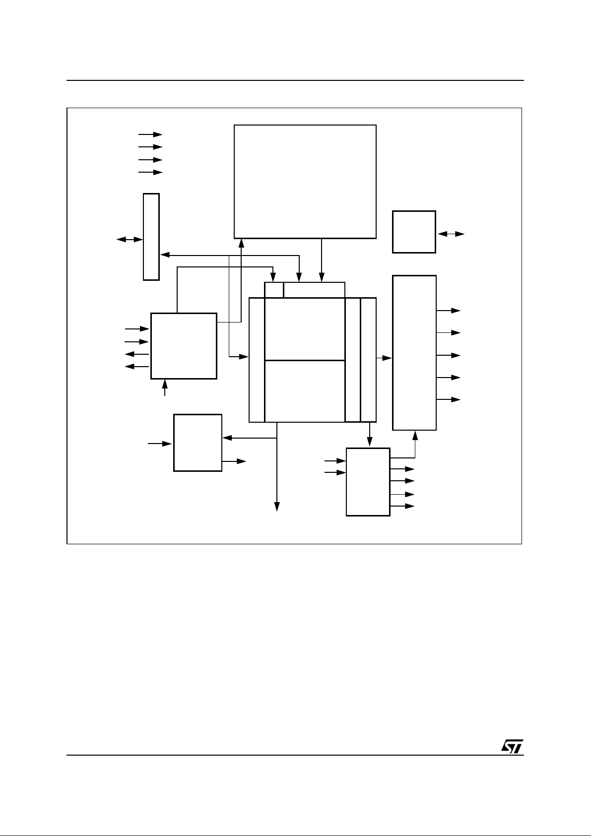
Figure 4, page 10 shows t he block diagram for the
M7040N device.
Part Number
M7040N-100ZA1 1.65V 2.5 or 3.3V 100MHz Commercial
M7040N-083ZA1 1.5V 2.5 or 3.3V 83MHz Commercial
M7040N-066ZA1 1.5V 2.5 or 3.3V 66MHz Commercial
Operating
Supply Voltage
Operating I/O
Voltage
Speed Temperature Range
Figure 2. Switch/Router Implementation Using the M7040N
System Bus
Network Line Interfaces
Switch
Fabric
Program
Memory
Switch
Processor
Host
ASIC
Search
Engine
SRAM
Bank
AI04272
7/159
Page 8
M7040N
Table 2. Signal Names
Symbol
CLK_MODE
CLK2X_CLK1X I Master Clock
PHS_L I Phase
TEST_CO
(2)
TEST I Test Input (ST Use Only)
TEST_FM I Test Input (ST Use Only)
RST_L I Reset
TEST_PB
(3)
CFG_L I Configuration
Command and DQ Bus
CMD[10:0] I Command Bus
CMDV I Command Valid
DQ[71:0] I/O Address/Data Bus
(4)
ACK
(4)
EOT
SSF T SEARCH Successful Flag
SSV T
MULTI_HIT O Multiple Hit Flag
HIGH_SPEED I 100MHz Indicator
CLKTUNE[3:0] I PLL Tuner
Type
(1)
Description
Clocks and Reset
I Clock Mode
I Test Output (ST Use Only)
I Test Input (ST Use Only)
T READ Acknowledge
T End of Transfer
SEARCH Successful Flag
Valid
SRAM Interface
SADR[23:0] T SRAM Address
CE_L T SRAM Chip Enable
WE_L T SRAM Write Enable
OE_L T SRAM Output Enable
ALE_L T Address Latch Enable
Cascade Interface
LHI[6:0] I Local Hit In
LHO[1:0] O Local Hit Out
BHI[2:0] I Block Hit In
BHO[2:0] O Block Hit Out
FULI[6:0] I Full In
FULO[1:0] O Full Out
FULL O Full Flag
Device Identification
ID[4:0] I Device Identification
Supplies
Chip Core Supply (1.5V for
V
DD
n/a
66 and 83MSPS; 1.65 for
100MSPS)
V
DDQ
Chip I/O Supply (2.5 or
n/a
3.3V)
Test Access Port
TDI I
TCK I
Test Access Port’s Test
Data In
Test Access Port’s Test
Clock
TDO T
TMS I
TRST_L I Test Access Port’s Reset
Note: 1. Signal types are: I = Input only; I/O = Input or Output; O = Output; and T = Tristate
See DESCRIPTIONS FOR CONNECTION DIAGRAM (Figure 3, page 9), page 152 for individual connection details.
2. In the previous versions of this specification, this signal was called, “CLK_OUT.”
3. In previous versions of this specification, this signal was called, “PLL_BYPASS.”
4. ACK and EOT Signals require a weak, external pull-down resistor of 47 KΩ or 100 KΩ.
8/159
Test Access Port’s Test
Data Out
Test Access Port’s Test
Mode Select
Page 9
Figure 3. Connections
123456789
CLK
V
TDI
TCK
ID0
ID1
ID3
LHI0
LHI2
LHI6
LHO0
DDQ
BHI1
DDQ
DDQ
FULL
V
TEST
CO
DQ71
DDQ
V
DQ69
SS
V
TMS
V
TDO
L
V
V
DDQ
V
ID2
V
ID4
LHI1
NC1
V
LHI3
LHI4
LHI5
V
LHO1
V
BHI0
V
BHI2
MULTI_
V
HIT
V
BHO1
V
V
SS
V
FULI1
DDQ
FULI4FULI3
FULI5
NC2
V
FULO0
V
V
DDQ
V
ACK
V
EOT
SS
V
V
DDQ
V
DQ70
SS
CLK
DQ68
TUNE2
DD
DD
DD
DD
DDQ
DQ63
DQ67
DQ61
DQ65
V
V
DD
DD
V
V
SS
SS
V
SS
V
SS
V
SS
DD
V
SS
V
SS
V
SS
V
DD
DD
V
DD
DD
V
DD
DD
V
DD
DD
V
DD
DD
V
DD
DD
V
SS
V
SS
V
SS
V
SS
DD
V
SS
DD
V
DD
SS
VSSV
DD
SS
V
V
DD
DD
DD
DQ64
V
DDQ
DQ66
DQ62
1234567 8 91011
AA
AB
AC
AD
AE
A
TUNE3
B
C
TRST_
D
E
F
G
H
J
K
L
V
M
N
BHO0
P
V
R
BHO2
T
FULI0
U
FULI2
V
V
W
FULI6
Y
FULO1
RST_L
TEST_
AF
V
DDQ
DQ59
V
V
V
V
DQ60
V
DDQ
M7040N
11
10
DQ53
DQ57
V
DQ55
DDQ
V
NC8
DD
DD
V
V
SS
SS
V
V
SS
SS
V
NC3
DD
DD
DQ54
DQ58
DQ56
DQ52
DQ43
DQ51
DQ45
DQ47
V
DQ49
DDQ
V
V
V
DQ50
DQ48
V
DDQ
SS
SS
V
SS
SS
DQ46
DQ44
V
DDQ
SS
SS
12 13 14 15 16
DQ35
DQ37
DQ41
V
DDQ
DQ39
V
V
V
V
V
V
DQ42
DQ40
DQ33
V
V
DD
DD
DD
V
V
V
V
V
V
V
V
V
V
DQ38
DQ36
DD
DD
V
SS
SS
V
SS
SS
V
SS
SS
V
SS
SS
V
SS
SS
V
SS
SS
V
DD
DD
V
DD
DD
V
DDQ
DQ34
DD
SS
V
SS
V
SS
SS
V
SS
V
SS
DD
DD
12 13 14 15
DQ31
DQ29
V
V
V
V
V
V
V
V
V
DQ32
DQ30
DQ17
DQ15
DQ13
V
V
DQ16
DQ18
DQ14
19
V
DDQ
DQ11
NC7
V
SS
V
SS
NC4
DQ12
V
DDQ
19 20
17 18
V
DQ25
DDQ
DQ27
V
DD
VDDV
DD
VSSV
SS
V
SS
V
SS
V
SS
V
SS
VSSV
SS
V
DD
V
DD
DQ28
V
DDQ
DQ21
V
DDQ
DQ23
V
DQ19
DD
DD
V
V
DD
SS
SS
V
SS
SS
V
SS
SS
V
SS
SS
V
SS
SS
SS
V
V
DD
DD
DD
V
DQ26
DQ24
16
DD
SS
DQ20
V
DDQ
DQ22
17 18
21
20
DQ9
DQ7
V
V
SS
V
SS
V
DQ10
DQ8
22 23 24
TEST_
DQ3
DQ5
V
DD
SS
SS
DD
TEST_
DQ1
DDQ
V
V
V
DQ6
DQ4
21
V
V
DD
DD
V
V
SS
SS
V
V
V
V
V
V
V
V
V
V
V
V
V
V
V
VSSV
SS
V
V
DD
DD
V
DQ0
DDQ
DQ2
22 23 24 25 26
25 26
CLK
HIGH_
V
DDQ
FM
SPEED
V
CFG_L
PB
SADR
V
DD
DD
SADR
V
SS
DD
SADR
V
SS
DD
SADR
V
SS
DD
SADR
V
DD
SS
V
NC6
SS
SADR
SADR
SS
11
SADR
V
SS
13
SADR
V
DD
DD
V
V
DD
DD
SADR
V
DD
DD
SADR
V
DD
DD
SADR
V
DD
DD
CLK_
V
DD
DD
MODE
PHS_L
OE_L
SS
V
V
CE_L
SS
V
NC5
CMDV
SS
V
V
CMD1
SS
DD
V
V
CMD3
SS
DD
V
CMD5
SS
DD
V
CMD6
SS
DD
V
CMD8
DD
DD
V
V
DDQ
SSFSSV
CMD10
5
DDQ
12
DDQ
15
DDQ
19
21
22
DDQ
A
TUNE0
SADR
B
SS
0
V
C
DDQ
1
SADR
D
2
3
SADR
E
4
V
F
DDQ
6
SADR
G
8
7
SADR
H
9
SADR
J
10
SADR
K
14
SADR
L
16
SADR
M
17
SADR
N
18
SADR
P
20
V
R
DDQ
SADR
T
23
CLK1x/
U
CLK2x
WE_L
V
ALE_L
W
CMD0
Y
CMD2
AA
CMD4
AB
V
AC
DDQ
CMD7
AD
CLK
AE
SS
TUNE1
AF
CMD9
AI04646
9/159
Page 10
M7040N
Figure 4. M7040N Block Diagram
PHS_L
CLK1X_CLK2X
RST_L
CLK_MODE
DQ [71:0]
Compare/PIO Data
CMD [10:0]
CMDV
ACK
EOT
Command
Decode
and PIO Access
ID [4:0]
Comparand Registers[15:0]
Global Mask Registers [15:0]
Information and Command Register
Burst Read Register
Burst Write Register
Next Free Address Register
Search Successful Index Registers [7:0]
(All registers are 72-bit-wide)
Compare/PIO Data
Cmd
Configurable as
128K x 36
64K x 72
32K x 144
16K x 288
Data Array
Configurable as
128K x 36
Address Decode
Priority Encode
64K x 72
32K x 144
16K x 288
Mask Array
Match Logic
TAP
Controller
Pipeline
and
SRAM
Control
TAP
SADR [23:0]
OE_L
WE_L
CE_L
ALE_L
Full LogicFULL [6:0]
FULL
LHI [6:0]
BHI [2:0]
FULO [1:0]
Arbitration
Logic
LHO [1:0]
BHO [2:0]
SSF
SSV
AI04645
10/159
Page 11
M7040N
MAXIMUM RATING
Stressingthedeviceabovetheratinglistedinthe
“Absolute Maximum Ratings” table may cause
permanent damage to the device. These are
stress ratings only and operation of t he dev ice at
these or any other conditions above those indicated in the Operating sections of this specification is
Table 3. Absolute Maximum Ratings
Symbol Parameter Value Unit
T
STG
(1)
T
SLD
V
DD
V
DDQ
V
DDQ
V
DDQ
I
O
Note: 1. Solderingtemperaturenotto exceed260°C for 10 seconds (total thermal budget not to exceed 150°C for longer than 30 seconds).
Storage Temperature (VDDOff)
Lead Solder Temperature for 10 seconds 235 °C
VDDOperating Supply Voltage
V
Voltage for I/O (3.3V)
DDQ
V
Voltage for I/O (2.5V)
DDQ
V
Voltage for I/O (1.8V)
DDQ
Output Current 100 mA
not implied. Exposure to Absolute Maximum Ra ting conditions for extended periods m ay affect device reliability. Refer also to the
STMicroelectronics SURE Program and other relevant quality documents.
–0to70 °C
CLK1X = 83MHz 1.575 V
CLK1X = 100MHz 1.733 V
3.5 V
2.625 V
1.9 V
11/159
Page 12
M7040N
DC AND AC PARAMETERS
This section summarizes the operating and m easurement conditions, as well as the DC and AC
characteristics of the device. The parameters in
the following DC and AC Charact eristic tables are
derived from tests performed under the Measure-
Table 4. DC and AC Measurement Conditions
Sym Parameter Min Max Units
ment Conditions listed i n the relevant tables. Designers should check that the operating conditions
in their projects match the measurement co nditions when using the quoted parameters.
V
DDVDD
V
DDQVDDQ
V
DDQVDDQ
V
DDQVDDQ
t
A
Operating Supply Voltage
Voltage for I/O (3.3V)
Voltage for I/O (2.5V)
Voltage for I/O (1.8V)
Ambient Operating Temperature 0 70 °C
Supply Voltage Tolerance –5+5%
Input Pulse Levels (V
Input Pulse Levels (V
Input Pulse Levels (V
DDQ
DDQ
DDQ
= 3.3V)
= 2.5V)
= 1.8V)
Input Rise and Fall Times at 0.3V and 2.7V (V
Input Rise and Fall Times at 0.25V and 2.25V (V
Input Timing Reference Levels (V
Input Timing Reference Levels (V
Input Timing Reference Levels (V
Output Timing Reference Levels (V
Output Timing Reference Levels (V
Output Timing Reference Levels (V
DDQ
DDQ
DDQ
DDQ
DDQ
DDQ
= 3.3V)
= 2.5V)
= 1.8V)
Output Load
Note: 1. Maximum allowable applies to overshoot only (V
2. Minimum allowable applies to undershootonly.
CLK1X = 83MHz 1.425 1.575 V
CLK1X = 100MHz 1.568 1.733 V
3.1 3.5 V
2.375 2.625 V
1.7 1.9 V
GND to 3.0 V
GND to 2.5 V
GND to 1.8 V
DDQ
= 3.3V)
DDQ
= 2.5V)
≤ 2ns (see Figure 6,
page 13)
≤ 2ns (see Figure 6,
page 13)
1.5 V
1.25 V
0.9 V
= 3.3V)
= 2.5V)
= 1.8V)
1.5 V
1.25 V
0.9 V
(see Figure 5 and
Figure 7, page 13)
is 3.3Vsupply).
DDQ
ns
ns
V
12/159
Page 13
Figure 5. M7040N 1.8, 2.5, or 3.3V AC Testing Load
50ΩZ0 = 50Ω
M7040N
D
OUT
VL= 1.25V for V
VL= 1.50V for V
C
L
Figure 6. M7040N 1.8, 2.5, or 3.3V Inp ut Waveform
+2.5V V
+3.0V V
DDQ
DDQ
= 2.5V /
= 3.3V
90%
10%
GND
Figure 7. M7040N 1.8, 2.5, or 3.3V I/O Output Load Equivalent
V
DDQ
DDQ
DDQ
90%
10%
AI04752
= 2.5V
= 3.3V
AI04751
208Ω for V
158Ω for V
DDQ
DDQ
= 2.5V
= 3.3V
Q
192Ω for V
175Ω for V
Note: 1. Output loading is specified with CL = 5pF as in Figure 7. Transition is measured at ± 200 mV from steady-state voltage.
2. TheloadusedforV
testing is shown in Figure 7.
OH,VOL
DDQ
DDQ
= 2.5V
= 3.3V
5pF
For Hi-Z and VOL/V
OH
(1, 2)
AI04753
13/159
Page 14
M7040N
Table 5. Capacitance
Symbol Parameter
C
IN
C
IO
Note: 1. Effectivecapacitance measured withpower supply. Sampled only, not100% tested.
2. At 25°C, f = 1MHz.
3. Outputs deselected.
Input Capacitance
(3)
Output Capacitance
Test Condition
V
IN
V
OUT
Table 6. DC Characteristics
Sym Parameter
Test Condition
(1,2)
=0V
=0V
(1)
Min Max Unit
6pF
6pF
Min Max Unit
Input Leakage Current
I
LI
I
Output Leakage Current
LO
Input Low Voltage (V
V
IL
Input High Voltage (V
V
IH
Input Low Voltage (V
V
IL
Input High Voltage (V
V
IH
Input Low Voltage (V
V
IL
Input High Voltage (V
V
IH
Output Low Voltage (V
V
OL
Output High Voltage (V
V
OH
Output Low Voltage (V
V
OL
Output High Voltage (V
V
OH
Output Low Voltage (V
V
OL
Output High Voltage (V
V
OH
DDQ
DDQ
DDQ
1.65V Supply Current at VDD(max)
1.5V Supply Current at V
I
DD1
1.5V Supply Current at V
V
DDQ=VDDQ
V
DDQ=VDDQ
= 3.3V)
= 3.3V)
DDQ
= 2.5V)
= 2.5V)
DDQ
= 1.8V)
= 1.8V) 0.7 * V
DDQ
= 3.3V) V
DDQ
= 3.3V) V
DDQ
= 2.5V) V
DDQ
= 2.5V) V
DDQ
= 1.8V) V
DDQ
= 1.8V) V
DDQ
(max)
DD
(max)
DD
(max), VIN= 0 to V
(max), VIN= 0 to V
DDQ=VDDQ
DDQ=VDDQ
DDQ=VDDQ
DDQ=VDDQ
DDQ=VDDQ
DDQ=VDDQ
(min), IOL= 16mA
(min), IOH= 8mA
(min), IOL=8mA
(min), IOH= 8mA
(min), IOL=8mA
(min), IOH= 8mA VDD– 0.45
100MHz Search Rate 6.0 A
83MHz Search Rate 5.0 A
66MHz Search Rate 4.0 A
100MHz Search Rate, I
I
3.3V Supply Current at VDD(max)
DD2
83MHz Search Rate, I
66MHz Search Rate, I
100MHz Search Rate, I
2.5V Supply Current at VDD(max)
I
DD2
83MHz Search Rate, I
66MHz Search Rate, I
Note: 1. Valid for Ambient Operating Temperature: TA=0to70°C; VDD=1.5V.
OUT
OUT
OUT
OUT
OUT
OUT
DDQ
DDQ
=0mA
=0mA
=0mA
=0mA
=0mA
=0mA
(max)
(max)
–10 +10 µA
–10 +10 µA
–0.3 0.8 V
V
2.0
DDQ
+0.3
–0.3 0.7 V
V
1.7
–0.3
DDQVDDQ
DDQ
0.35 * V
+0.3
DDQ
+0.3
0.4 V
2.4 V
0.4 V
2.0 V
0.45 V
350 mA
300 mA
240 mA
350 mA
300 mA
240 mA
V
V
V
V
V
14/159
Page 15
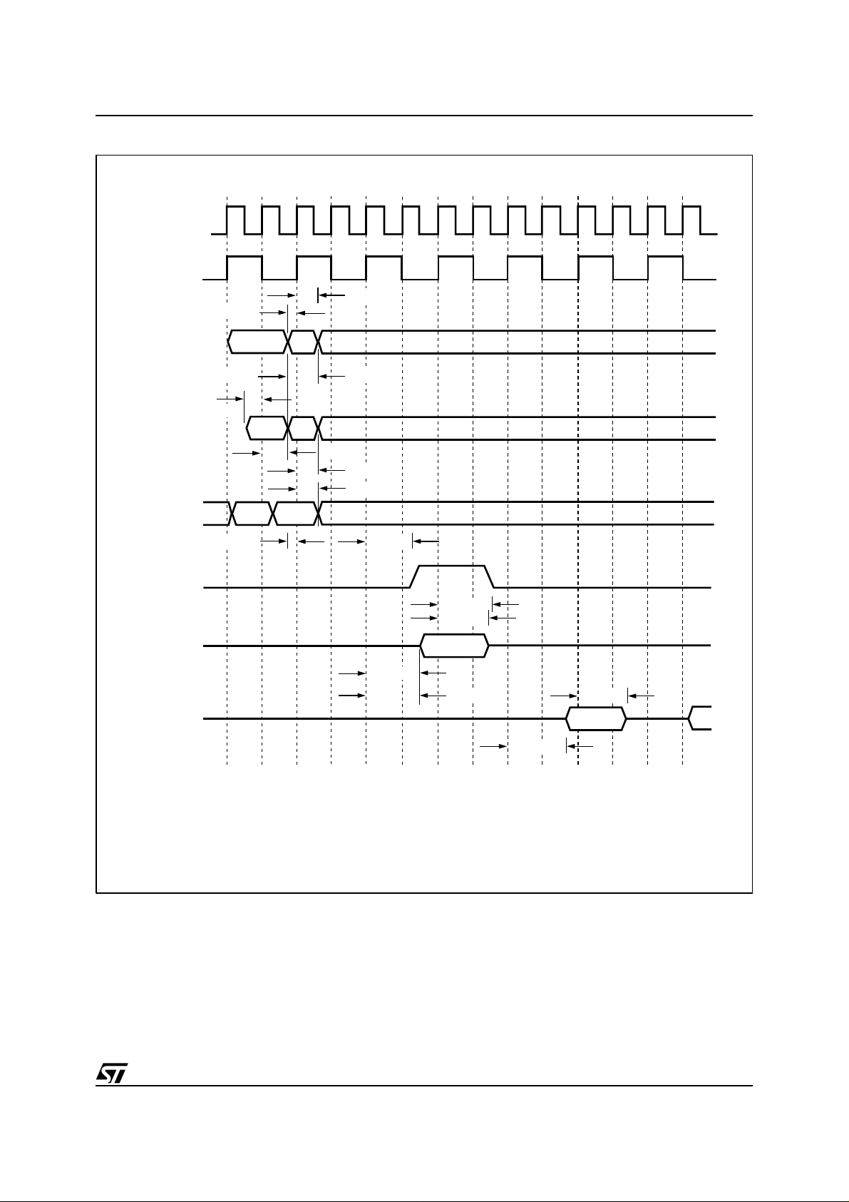
Figure 8. AC Tim ing Waveforms with CLK2X
M7040N
CLK2X
CLK
Signal
Group 0
Signal
Group 1
Signal
Group 2
Signal
Group 3
Signal
Group 4
Signal
Group 5
tISCH
tISCH
tICSCH
Cycle
0
tISCH
Cycle
1
Cycle
2
Cycle
tIHCH
3
tIHCH
tIHCH
tIHCH
tICHCH
tCKHOV
Cycle
4
tCKHSV
Cycle
5
Cycle
6
tCKHOV
tCKHSHZ
tCKHSLZ
Cycle
7
Cycle
8
tCKHDV
Cycle
9
Cycle
10
tCKHDZ
Cycle
11
Cycle
12
Signal Group 0: PHS_L, RST_L
Signal Group 1: DQ, CMD, CMDV
Signal Group 2: LHI, BHI, FULI
Signal Group 3: LHO, BHO, FULO, FULL
Signal Group 4: SADR, CE_L, OE_L, WE_L, ALE_L, SSF, SSV
Signal Group 5: DQ, ACK, EOT
AI04748
15/159
Page 16
M7040N
Figure 9. AC Tim ing Waveforms with CLK1X
CLK1X
CLK
Signal
Group 0
Signal
Group 1
Signal
Group 2
Signal
Group 3
Signal
Group 4
Signal
Group 5
tISCH
tISCH
tICSCH
Cycle
0
tISCH
Cycle
1
Cycle
2
Cycle
tIHCH
3
tIHCH
tIHCH
tICHCH
tCKHOV
Cycle
4
tCKHSV
Cycle
5
Cycle
6
tCKHOV
tCKHSHZ
tCKHSLZ
Cycle
7
Cycle
8
tCKHDV
Cycle
9
Cycle
10
tCKHDZ
Cycle
11
Cycle
12
Signal Group 0: PHS_L, RST_L
Signal Group 1: DQ, CMD, CMDV
Signal Group 2: LHI, BHI, FULI
Signal Group 3: LHO, BHO, FULO, FULL
Signal Group 4: SADR, CE_L, OE_L, WE_L, ALE_L, SSF, SSV
Signal Group 5: DQ, ACK, EOT
16/159
AI04749
Page 17
Table 7. AC Timing Parameters with CLK2X
M7040N-
066
Row Sym
(V
DDQ
3.3V, 2.5V)
Min Max Min Max Min Max
f
1
CLOCK
t
2
CLOK
t
3
CKHI
t
4
CKLO
t
5
ISCH
t
6
IHCH
t
7
ICSCH
t
8
ICHCH
t
9
CKHOV
t
10
CKHDV
t
11
CKHDZ
t
12
CKHSV
t
13
CKHSHZ
t
14
CKHSLZ
Note: 1. Valid for Ambient Operating Temperature: TA=0to70°C; VDD=1.5V.
2. Values are based on 50% signal levels.
3. Based on an AC load of CL = 30pF (see Figure 5, Figure 6, and Figure 7, page 13).
4. These parameters are sampled and not 100% tested, and are based on an AC load of 5pF.
40 133 40 166 40 200 MHz CLK2X frequency
3.0 2.4 2.0 ns
3.0 2.4 2.0 ns
2.5 1.8 1.5 ns
0.6 0.6 0.5 ns
4.2 3.5 3.0 ns
0.6 0.6 0.5 ns
7.0 6.5 6.0 ns
=
M7040N-
083
(V
DDQ
3.3V, 2.5V,
1.8V)
=
M7040N-
100
=
(V
DDQ
3.3V, 2.5V)
Unit
0.5 0.5 0.5 ms PLL lock time
CLK2X high pulse
CLK2X low pulse
Input Setup Time to CLK2X rising edge
Input Hold Time to CLK2X rising edge
Cascaded Input Setup Time to CLK2X rising
(2)
edge
Cascaded Input Hold Time to CLK2X rising edge
8.5 7.0 6.5 ns
9.0 7.5 7.0 ns
8.5 7.0 6.5 ns
9.0 7.5 7.0 ns
6.5 6.0 5.5 ns
Rising edge of CLK2X to LHO, FULO, BHO, FULL
(3)
valid
Rising edge of CLK2X to DQ valid
Rising edge of CLK2X to DQ high-Z
Rising edge of CLK2X to SRAM bus valid
Rising edge of CLK2X to SRAM bus high-Z
Rising edge of CLK2X to SRAM bus low-Z
Description
(2)
(2)
M7040N
(1)
(2)
(2)
(2)
(3)
(4)
(3)
(4)
(4)
17/159
Page 18
M7040N
Table 8. AC Timing Parameters with CLK1X
Row Sym
f
1
CLOCK
t
2
CLOK
t
3
4
5
6
7
8
CKHI
t
CKLO
t
ISCH
t
IHCH
t
ICSCH
t
ICHCH
M7040N-
066
(V
DDQ
3.3V, 2.5V,
1.8V)
Min Max Min Max Min Max
20 66 20 83 20 100 MHz CLK1X frequency
6.75 5.4 4.5 ns
6.75 5.4 4.5 ns
2.5 1.8 1.5 ns
0.6 0.6 0.5 ns
4.2 3.5 3.0 ns
0.6 0.5 0.5 ns
M7040N-
M7040N-
083
=
(V
=
DDQ
3.3V, 2.5V,
1.8V)
(V
3.3V, 2.5V)
0.5 0.5 0.5 ms PLL lock time
100
DDQ
=
Unit
CLK1X high pulse
CLK1X low pulse
Description
(2)
(2)
Input Setup Time to CLK1X edge
Input Hold Time to CLK1X edge
(1)
(2)
(2)
Cascaded Input Setup Time to CLK1X rising
(2)
edge
Cascaded Input Hold Time to CLK1X rising
(2)
edge
t
9
CKHOV
t
10
CKHDV
t
11
CKHDZ
t
12
CKHSV
t
13
CKHSHZ
t
14
CKHSLZ
Note: 1. Valid for Ambient Operating Temperature: TA=0to70°C; VDD=1.5V.
2. Values are based on 50% signal levels and a 50/50% duty cycle of CLK1X.
3. Based on an AC load of CL = 30pF (see Figure 5, Figure 6, and Figure 7, page 13).
4. These parameters are sampled and not 100% tested, and are based on an AC load of 5pF.
8.5 7.0 6.5 ns
9.0 7.5 7.0 ns
8.5 7.0 6.5 ns
9.0 7.5 7.0 ns
6.5 6.0 5.5 ns
7.0 6.5 6.0 ns
Rising edge of CLK1X to LHO, FULO, BHO, FULL
(3)
valid
Rising edge of CLK1X to DQ valid
Rising edge of CLK1X to DQ high-Z
Rising edge of CLK1X to SRAM bus valid
Rising edge of CLK1X to SRAM bus high-Z
Rising edge of CLK1X to SRAM bus low-Z
(3)
(4)
(3)
(4)
(4)
18/159
Page 19

OPERATION
Command Bus and DQ Bus
CMD[10:0] c arries the command and its associated parameter. DQ[71:0] is used for data transfer t o
and from the database entries. These entries comprise a data and a mask field that are organized as
data and mask arrays. The DQ Bus carries the
search data (of the data and mask arrays and internal registers) during the SEARCH command as
well as the address and data during READ and/or
WRITE operations. The DQ Bus can also carry the
address information for the flow-through a ccesses
to the external SRAMs and/or SS R AMs.
Database Entry (Data Array and Mask Array)
Eachdatabas e entry comprises a data and a mask
field. The resultant value of the entry is “1,”“0,” or
“X(don’t care),” depending on the value in the data
and mask bits. The on-chip priority encoder selects the first matching entry in the database that
is nearest to location “0.”
Arbitration Logic
When multiple Search Engines are cascaded to
create large databases, the databeing searched is
presented to all Search Engines simultaneously in
the cascaded system. If multiple matches occur
within t he cascaded devices, arbitration logic on
the Search Engines will enable the winning device
(witha matching entrythat is closest to address “0”
of the cascaded database) t o drive th e SRAM bu s.
Pipeline and SRAM Control
Pipeline latency is added to give enough time to a
cascaded system’s arbitration logic to determine
the device that will drive the index of the mat ching
entry on the SRAM bus. Pipeline logic adds latency to both the SRAM access cycles and the SSF
and SSV signals to align them to the host ASIC receiving the associated data.
Full Logic
Bit[0] in each of the 72-bit entries has a special
purpose for the LEARN command (0 = empty, 1 =
full). When all the data entries have bit[0] = 1, the
database asserts the FULL Fl ag, indicating all the
Search Engines in the depth-cascaded array are
full.
Connection Des cri ptions
CLOCK MODE (CLK_MODE). This signal allows
the selection of clock input to the CLK1X/CLK2X
pin. If the CLK_MODE pin is low, CLK2X must be
supplied on that pin. PHS_L must also be sup-
M7040N
plied. If the C LK _MODE pin is high, CLK1X must
be supplied on the CLK2X/CLK1X pin, and the
PHS_L signal is not required. When the
CLK_MODE is hi gh, PHS_L is unused and should
be externally grounded.
Master Clock (CLK2X/CLK1X). Depending on
the C LK_MODE pin, either the CLK2X or the
CLK1X must be supplied. M7040N samples c ontrol and data signals on both the edges of CLK1X
if CLK1X is supplied. M7040N samples all the dat a
and control pins on the positive edge of CLK2X if
the CLK2X and P H S_L signals are supplied. All
signals are driven out of the device on the rising
edge of CLK1X if CLK1X is supplied, and are driven on the rising edge of CLK2X (when PHS_L is
low) if CLK2X is supplied.
Phase (PHS_L). This signal runs at half the frequency of CLK2X and generates an internal clock
from CLK2X (see Figure 10, page 21).
Test Output (TEST_CO). This is test output and
will stay unconnected in the application of the device.
Test Input (TEST). This signal should be c onnected to ground.
Test Input (TEST_FM). This signal s hould be
connected to ground.
Reset (RST_L). Driving RST_L low initializes the
device to a known state.
Test Input (TEST_PB). This signal should be
connected to ground.
Configuration. When CFG_L is low, M7040N will
operate in backward compatibility mode with
M7010 and M7020. When CFG_L is low, the
CMD[10:9] should be externally grounded. With
CFG_L low, t he device will b ehav e identically with
M7010 and M7020, and the new feature added to
M7040N will be disabled.
When CFG_L is high, the additional command
CMD[10:9] c an be used and the following additional features will be supported:
1. 16 pairs of Global Mas ks are supported instead
of eight;
2. Parallel WRITE to the data and mask arrays is
supported (se e Parallel WRITE, page 38); and
3. conf iguring tables of up to three different widths
does not require table identification bits in the
data array, thus sav ing two bits from each 72-bit
19/159
Page 20

M7040N
Command Bus (CMD[10:0]. [1:0] specifies the
command; [10:2] contains the command parameters. The descriptions of individual commands explains the details of the parameters. The encoding
of commands based on the [1:0] field are:
– 00: PIO READ
– 01: PIO WRITE
– 10 : SEARCH
– 11: LEARN
Command Valid (
CMDV). Qualifies the CMD bus
as follows:
– 0: No Co mmand
– 1: Command
Address/Data Bus (
DQ[71:0]). Carries the Read
and WRITE address as well as the data during
register, data, and mask array operations. It carries the comp are data during s earc h operations. It
also carries the SRAM address during SRAM PIO
accesses.
READ Acknowledge (ACK). Indicates that valid
data is available on the DQ Bus during register,
data, and mask array READ operations, or t he
data is available on t he SRAM data bu s during
SRAM READ operations.
Note: ACK Signals require a weak external pulldown resistor such as 47 or 100 KΩ.
End of Transfer (EOT). Indicates the end of
burst t ra ns fer during READ or WRITE burst operations.
Note: EOT Signals require a weak external pulldown resistor such as 47 KΩ or 100 KΩ.
SEARCH Succ essful Flag (SSF). When ass erted, t his signal indicates that the devi ce is the global winner in a SEARCH operation.
SEARCH Succ essful Flag Valid (SSV). W hen
asserted, this signal qualifies the SSF signal.
Multiple Hit Flag (MULTI_HIT). When asserted,
this signal indicates that there is more t han one location having a match on this device.
High Speed (HIGH_SPEED). When this signal is
high, the device willrun up to100MHzand perform
100 million searches per second. However, in this
mode, a T LSZ value of '00' is not supported in a
system of a single device. Furthermore, the device
will only support a TLSZ of '00' and '01' if more
than one device is cascaded to form database tables.
Clock Tune [3:0] (CLK_TUNE[3:0]). These test
pins should be set to logic level 1001.
SRAM Address (SADR[23:0]). This bus con-
tains address lines to access off-chip SRAMs that
contain ass ociative data. See Table 52, page 128
for the details of the generated SRAM address. In
a database of multiple M7040Ns, each corresponding bit of SADR from all cascaded devices
must be connected.
SRAM Chip Enable (CE_L). This is Chip Enable
control for external S R AMs. I n a database of multiple M7040Ns, CE_L of all cascaded devices
must be connected. This s ignal is then driven by
only one of the devices.
SRAMWriteEnable(WE_L). This is Write Enable co ntrol for external SRAMs. In a database of
multiple M7040Ns, WE_L of all cascaded dev ices
must be connected together. This signal is then
driven by only one of the devices.
SRAM Output Enable (OE_L). This is Output
Enable control for external SRAMs. Only the last
device drives this signal (with the LRA M bit set).
Address Latch Enable (ALE_L). When this signal is low, the addresses are valid on the SRAM
Address Bus. In a database of multiple M7040Ns,
the ALE_L of all cascaded dev ices must be connected. Th is signal is then driven by only one of
the devices.
Local Hit In (LHI[6:0]). These pins depth-cascade the device t o form a larger t able size. One
signal of th is bus is connected to the LHO[1] or
LHO[0] of each of the upstream devices in a bloc k.
Connect all unused LHI pins to a logic '0.' (For
more information, see DEPTH-CASCADING,
page 124.)
Local Hit Out (LHO[1:0]). LHO[1] and LHO[0]
are the same logical signal. LHO[1] or LHO[0] is
connected to one input of the LHI bus of up to four
downstream devices (in a block that contains up to
eight devices). (For more information, see
DEPTH-CASCADING, page 124.)
Block Hit In (BHI[2:0]). Input s from t he previous
BHO[2:0] are tied to the BHI[2:0] of the c urrent device (see DEPTH-CASCADING, page 124). In a
four-block system, the last block can contain only
seven devices because the ID code 11111 is used
for broadcast access.
Block Hit Out (BHO[2:0]). These outputs from
the last device in a block are connected to the
BHI[2:0] inputs of the devices in the downstream
blocks (see DE PTH-CA SC ADING, page 124).
20/159
Page 21
M7040N
Full In (FUL I[6:0]). Each signal in this bus is con-
nected to FULO[0] or FULO[ 1] of an ups tream device to generate the FULL s ignal f or the depthcascaded block. For more information, see
DEPTH-CASCADING, page 124 to Generate Full
for a Block Section.
Full Out (FULO[1:0]). FULO[1] and FULO[0] are
the same logical signal. One of these two signals
must be connected t o the FULI of up to four downstream devices in a depth-cascaded table. Bit [0]
in the data array indicates if the entry is f ull (1) or
empty (0).This sign al is asserted if all of the bits in
the data array are '1s.' Refer to Depth-Cascading
to Generate a “FULL” S ignal, page 124.
Full Flag (FULL). When asserted, this signal indicates that the table consisting of many depthcascaded devices is full.
Device Identification (ID[4:0]). The binary-en-
coded device I D for a depth-cascaded system
starts at 00000 and goes up to 11110. 11111 is re-
CLOCKS
If the CLK_MO D E pin is low, M7040N receives the
CLK2X and PHS_L signals. It uses the PHS_L signal to divide CLK2X and generate an internal clock
(CLK), as shown in Figure 10. The M7040N uses
CLK2X and CLK for internal operations. If the
CLK_MODE pin is high, the M7040N recei ves the
CLK1X only. the M7040N uses an internal PLL to
double the frequency of CLK1X and then divides
served for a special broadcast address that selects all casc aded search engines in the system.
On a broadcast read-only, the device with the
LDEV bit set to '1' responds.
Chip Core Supply (V
Chip I/O Supply (V
). This is equal to 1.5V.
DD
). This is equal to either
DDQ
2.5 or 3.3V.
Test Data In (TDI). This is the Test Access Port’s
Test Data In.
Test Clock (TCK). This is the Test Access Port’s
Test Clock.
Test Data Out (TDO). This is the Test Access
Port’s Test Dat a Out.
Test Mode Select (TMS). This is the Test Access Port’s Test Mode Select.
Test Reset (TRST_L). This is the Test Access
Port’s Test Res et.
thatclock by two to generate a CLK for internal operations, as shown in Figure 11.
Note: For the purpose of showing timing diagrams, all such diagram s in this document will be
shown in CLK2X mode. For a timing diagram in
CLK1X mode, the following substitution can be
made (see Figure 12).
Figure 10. Clocks (CLK2X and PHS_L)
CLK2X
PHS_L
(1)
CLK
Note: Any reference to “CLK Cycles” means 1 cycle of the signal, “CLK.”
1. “CLK” is an internal signal.
Figure 11. Clocks (CLK1X)
CLK1X
(1)
CLK
1. “CLK” is an internal signal.
AI04750
AI04665
21/159
Page 22
M7040N
Figure 12. Clocks for All Timing Diagrams
CLK2X
PHS_L
(Use for CLK1X MODE)
CLK1X
(Use for CLK1X MODE)
PLL USAGE
When the device first powers up, it takes 0.5 ms to
lock the internal phase-lock loop (PLL). During this
locking of the PLL, in addition to 32 extra CLK1X
cycles in CLK1X mode and 64 extra cycles in
CLK2X mode, the RST_L mu st be held low f or
proper initialization of the device. Setu p and hold
requirements will change in CLK1X mode if the
AI04666
duty cycle of the CLK1X is varied. All signals into
the device in CLK1X mode are sampled by a clock
that is generated by multiplying CLK1X by two.
Since PLL has a locking range, the de vice wi ll only
work between the range of frequencies spec ified
in the timing specification section.
REGISTERS
All r egisters in t he M7040N are 72 bits wide. The
M7040N contains 16 pairs of comparand storage
registers, 16 pairs of gl obal mas k registers
(GMRs), eight search successful index registers
and one each of command, information, burst
READ, burst WRITE, and next-free address registers. Table 9 provides an overview of all the
M7040N registers. The registers are ordered in ascending addres s order. Each register group is then
described in the following subsections.
Table 9. Register Overview
Address Abbreviation Type Name
0–31 COMP0–31 R
32–47, 96–111 MASKS RW 16 Global Mask Registers Pairs.
48–55 SSR0–7 R 8 SEARCH Successful Index Registers.
56 COMMAND RW Command Register.
57 INFO R Information Register.
58 RBURREG RW Burst Read Register.
59 WBURREG RW Burst Write Register.
60 NFA R Next Free Address Register.
61–63 ––Reserved
32 Comparand Registers. Stores comparands from the DQ Bus for
learning later.
22/159
Page 23
M7040N
Comparand Registers
The device contains 32 72-bit comparand registers (16 pairs) dynamically selected in every
SEARCH operation to store the comparand presented on t he DQ Bus. The LEARN command will
later use these registers when executed. The
M7040N stores the SEARCH command’sCycleA
comparand in the even-numbered regi ster and t he
Cycle B comparand in the odd-numbered register,
as shown in Figure 13.
Figure 13. Comparand Register Selection
During SEARCH and LEARN
Instructions
7272
Address
Index
143 0
0
1
0
6
1
32
54
7
Mask Registers
The device cont ains 32 72-bit global mask registers (16 pairs) dynamically selected in every
SEARCH operation to s elect the search subfield.
The addressing of these registers is explained in
Figure 14. The four-bit GMR Index supplied on t he
command (CMD) bus can apply 16 pairs of global
masks during the SEARCH and WRITE operations, as shown below.
Note: In 72-bit SEARCH and WRITE opera tions,
the host ASI C must program both the even and
odd mask registers with the same values.
Each mask bit in the GMRs is used during
SEARCH and WRITE operations. I n SEARCH operations, setting the mask bi t to '1' enables compares; setting the mask bit to '0' dis ables
compares (forced match ) at the corresp onding bit
position. In WRITE operations to the data or mask
array, sett ing the mask bit to '1' enables WRITEs;
setting the m as k bit to '0' disables WRITEs at the
corresponding bit position.
Figure 14. Addressing the Global Masks
RegisterArray
7272
Address
Index
143 0
15
30 31
AI04667
0
1
2
3
4
5
6
7
8
9
10
11
12
13
14
15
SEARCH and WRITE Command
0
6
8
10
12
14
16
18
20
22
24
26
28
30
Global Mask Selection
11
13
15
17
1
32
54
7
9
19
21
23
25
27
29
31
AI04668
23/159
Page 24
M7040N
SEARCH-Successful Registers (SSR[0:7])
The device contains eight search successful registers (SSRs) to hold the index of the location
where a successful search occurre d. The format of
each register is described in Table 10. T he
SEARCH command specifies which SSR stores
the index of a spec ific SEARCH command in Cycle B of the SEARCH Instruction. Subsequently,
the host ASIC can u se this register to access that
Table 10. SEARCH-Successful Register (SSR) Description
Field Range Initial Value Description
Index. This is the address of the 72-bit entry where a successful
search occurs. The device updates this field only when a search is
INDEX [15:0] X
– [30:16] 0 Reserved.
VALID [31] 0
– [71:32] 0 Reserved.
successful. If a hit occurs in a 144-bit entry-size quadrant, the LSB is
'0.' If a hit occurs in a 288-bit entry size quadrant, the two LSBs are
'00.' This index updates if the device is either a local or global winner
in a SEARCH operation.
Valid. During SEARCH operation in a depth-cascaded configuration,
the device that is a global winner in a match sets this bit to '1.' This bit
updates only when the device is a global winner in a SEARCH
operation.
data array, mask array, or ex ternal SRAM using
the index as part of the indirect access address
(see Table 20, page 34 and Table 23 , page 37)
The device with a valid bit set performs a REA D or
WRITE operation. All oth er dev ices suppress the
operation.
.
24/159
Page 25
The Command Register
Table 11. Command Register Field Descriptions
Field Range
SRST [0] 0
DEVE [1] 0
TLSZ [3:2] 01
HLAT [6:4] 000
LDEV [7] 0
Initial
Value
Software Reset. If '1,' this bit resets the device, with the same effect as the hardware
reset. Internally, it generates a reset pulse lasting for eight CLK cycles. This bit
automatically resets to a '0' the reset cycle has completed.
Device Enable. If '0,' it keeps the SRAM Bus (SADR, WE_L, CE_L, OE_L, and
ALE_L), SSF, and SSV signals in 3-state condition and forces the cascade interface
output signals LHO[1:0] and BHO[2:0] to '0.' It also keeps the DQ Bus in input mode.
The purpose of this bit is to make sure that there are no bus contentions when the
devices power up in the system.
Table Size. The host ASIC must program this field to configure the chips into a table
of a certain size. This field affects the pipeline latency of the SEARCH and LEARN
operations as well as the READ and WRITE accesses to the SRAM (SADR[23:0],
CE_L, OE_L, WE_L, ALE_L, SSV, SSF, and ACK). Once programmed, the search
latency stays constant.
Latency # CLK Cycles
with HIGH_SPEED low
00: 1 device 4
01: 2-8 devices 5
10: 9-31 devices 6
11: Reserved
Latency # CLK Cycles
with HIGH_SPEED high
00: Not supported
01: 1 devices 5
10: 2-31 devices 6
11: Reserved
Latency of Hit Signals. This field adds latency to the SSF and SSV signals during
SEARCH, and ACK signal during SRAM READ access by the following number of
CLK cycles.
000: 0 100: 4
001: 1 101: 5
010: 2 110: 6
011: 3 111: 7
Last device in the cascade. When set, this is the last device in the depth-cascaded
table and is the default driver for the SSF and SSV signals.
In the event of a search failure, the device with this bit set drives the hit signals as
follows:
SSF = 0, SSV = 1
During non-search cycles, the device with this bit set drives the signals as follows:
SSF = 0, SSV = 0
M7040N
Description
25/159
Page 26
M7040N
Field Range
LRAM [8] 0
CFG [24:9]
[71:25] 0 Reserved.
Initial
Value
0000
0000
0000
0000
Description
Last device on this SRAM Bus. When set, this device is the last device on this
SRAM bus in the depth-cascaded table and is the default driver for the SADR, CE_L,
WE_L, and ALE_L signals. In cycles where no M7040N device in a depth-cascaded
table drives these signals, this device drives the signals as follows:
SADR = FFFFFF,
CE_L = 1
WE_L = 1
ALE_L = 1
OE_L is always driven by the device for which this bit is set.
Database Configuration. The device is internally divided into eight quadrants of 8K x
72, each of which can be configured as 8K x 72, 4K x 144, or 2K x 288 as follows:
00: 8K x 72
01: 4K x 144
10: 2K x 288
11: low power, partition not used for SEARCH
Bits [10:9] apply to configuring the 1st quadrant in the address space.
Bits [12:11] apply to configuring the 2nd quadrant in the address space.
Bits [14:13] apply to configuring the 3rd quadrant in the address space.
Bits [16:15] apply to configuring the 4th quadrant in the address space.
Bits [18:17] apply to configuring the 5th quadrant in the address space.
Bits [20:19] apply to configuring the 6th quadrant in the address space.
Bits [22:21] apply to configuring the 7th quadrant in the address space.
Bits [24:23] apply to configuring the 8th quadrant in the address space.
The Information Register
Table 12. Information Register Field Descriptions
Field Range Initial Value Description
Revision [3:0] 0001
Implementation [6:4] 001 This is the M7040N implementation number.
Reserved [7] 0 Reserved.
Device ID [15:8] 00000100 This is the Device Identification Number.
MFID [31:16] 0000_0010_0000_1111
[71:32] Reserved.
Revision Number. This is the current device revision
number. Numbers start from one and increment by one
for each revision of the device.
Manufacturer ID. This field is the same as the
manufacturer ID and continuation bits in the TAP
controller.
26/159
Page 27
The Read Burst Address Register (RBURREG)
These READ burst address register f ields m ust be
programmed before burst read.
Table 13. Read Burst Register Description
Field Range Initial Value Description
Address. This is the starting address of the data array or mask array
ADR [15:0] 0
[18:16] Reserved.
BLEN [27:19] 0
[71:28] Reserved.
during a burst READ operation. It automatically increments by 1 for
each successive read of the data array or mask array. Once the
operation is complete, the contents of this field must be reinitialized
for the next operation.
Length of Burst Access. The device is capable of writing from 4 up
to 511 locations in a single burst. The BLEN decrements
automatically. Once the operation is complete, the contents of this
field must be reinitialized for the next operation.
The Write Burst Address Register (WBURREG)
These WRITE burst address register fields must
be programmed before burs t write.
M7040N
Table 14. Write Burst Register Description
Field Range Initial Value Description
Address. This is the starting address of the data array or mask array
during a burst WRITE operation. It automatically increments by 1 for
ADR [15:0] 0
[18:16] Reserved.
BLEN [27:19] 0
[71:28] Reserved.
each successive write of the data array or mask array. Once the
operation is complete, the contents of this field must be reinitialized for
the next operation.
Length of Burst Access. The device is capable of writing from 4 up
to 511 locations in a single burst. The BLEN decrements
automatically. Once the operation is complete, the contents of this
field must be reinitialized for the next operation.
The NFA Register
Bit [ 0] ofeach 72-bit data entry is a special bit designated f or use in the operation of the LEA R N
command. In 72-bit quadrants, the bi t[0] indicates
whether a location is full (bit set to'1') or empt y (bit
set to '0'). Every WRITE/LEARN command loads
the address of first 72-bit location that contains a
'0' in the entry ’s bit[0]. This is stored in the NFA
register(see Table 15). If all the bits in a device are
set to '1,' the M7040N asserts FULO[1:0] to '1.'
In 144-bit-configured quadrants, the LSB of this
set bit '0' and bit 72 in a 144-bit word t o either '0' or
'1' to indicate full/empty status.
Note: Both bits (0 a nd 72) must be set to '0' or '1'
(e.g., '10' or '01' settings are invalid).
Table 15. NFA Regi ster
Address 71 - 16 15 - 0
60 Reserved Index
register is always set to '0.' The host ASIC must
27/159
Page 28
M7040N
SEARCH ENGINE ARCHITECTURE
The M7040N consists of 64K x 72-bit storage c ells
referred to as d ata bits.There is a mask cell corresponding to each data cell. Figure 15 shows the
three organi zations of the device based on the value of the CFG bits in the command register.
During a SEARCH operation, the search data bit
(S), dat a array bit (D), mask array bit (M) and the
global mask bit (G) are used in the following manner to generate a match at that bit position (s ee
Table 16, page 29).
The entry with all matched bit positions results in a
successful search during a SEARCH operation.
In order for a successful search within a device to
make the device the local winner in the SEARCH
operation, all 72-bit positions must generate a
match for a 72-bit entry in 72-bit-configured quadrants, or all 144-bit positions must generate a
match for two consecutive ev en and odd 72-b it entries in quadrants configured a s 144 bits, or all
Figure 15. M7040N Database Width Configuration
288-bit positions must generate a m atch f or 4 consecutive entries aligned to 4 entry-pa ge boundaries of 72-bit entries in quadrants configured as
288 bits.
Anarbitration mechanism using a casc ade bus determines the global winning device among the local winning devices in a SEARCH cycle. The
global winning device drives t he SRAM Bus, SSV,
and the SS F signal s . In case of a SEARCH failure,
the devices with the LDEV and LRAM bits set
drive(s) the S RAM Bus, SSF, and SSV signals
The M7040N device can be configured to contain
tables of different widths, even within the same
chip. Figure 16, page 29 shows a sample configuration of different widths.
Data and Mask Addressing
Figure 17, page 29 shows the M7040N data array
and mask array addressing procedure.
72
64 K
CFG = 0000000000000000
Masks
Data
144
32 K
Masks
Data
CFG = 0101010101010101
288
16 K
CFG = 1010101010101010
Masks
Data
AI04669
28/159
Page 29
M7040N
Table 16. Bit Position Match Figure 16. Multi-width Configu ration Example
G M S D Match
0XXX1
10XX1
11001
11010
11100
11111
8 K
8 K
8 K
8 K
72
72
72
72
Figure 17. M7040N Data and Mask Array Addressing
72 7272 72 7272
71 0
0
1
2
3
64 K
283 0
16K
65532 65533 65534 65535
CFG = 1010101010101010
(288- bit conf igurat ion)
4 K
4 K
2 K
144
144
288
2 K 288
CFG = 10 10 01 01 11 11 00 00
Inactive (low power)
143 0
3210
7654
32K
AI04670
72
10
32
54
76
65535
CFG = 0000000000000000
(72-bit Conf ig uration)
65534 65535
CFG = 0101010101010101
( 144-bit Configu ration)
AI04671
29/159
Page 30
M7040N
COMMAND CODES AND PARAMETERS
A master device, such as an ASIC controller, issues c ommands to the M7040N using the Command Valid CMDV signal and the CMD Bus. The
following subsections describe the functions of the
commands.
Command Codes
The M70 40N implements four basic commands
shown in Table 17. The Com mand Code m us t be
presented to CMD[1:0] while keeping the command valid (CMDV) signal high for t wo CLK2X cycles. These two CLK2X cycles are designated as
“Cycle A” and “Cycle B” when the CLK_MODE pin
is low. In CLK2X mode, the controller ASIC must
Table 17. Command Codes
CMD Code Command Description
align the instructions with the PHS_L signal. The
command code must be presented to CMD[1:0]
while keeping the CMDV signal high for one
CLK1X cycle when the CLK_MODE pin is high. I n
CLK1X mode the high phase of the CLK1X is designated as Cycle A and the low phase of the
CLK1X is designated as C y cle B. The CMD[10:2]
field passes the parameters of the command in
Cycles A and B.
Commands and Command Parameters
Table 18, page 31 lists the CMD bus fields that
contain the M7040N command parameters as well
as their respective cycles.
00 READ
01 WRITE
10 SEARCH
11 LEARN
Reads one of the following: data array, mask array, device registers, or external
SRAM.
Writes one of the following: data array, mask array, device registers, or external
SRAM.
Searches the data array for a desired pattern using the specified register from the
global mask register array and local mask associated with each data cell.
The device has internal storage for up to 16 comparands that it can learn. The
device controller can insert these entries at the next free address (as specified by
the NFA register) using the LEARN Instruction.
30/159
Page 31

Table 18. Command Parameters
(1, 2)
Cmd
READ
WRITE
SEARCH
LEARN
Note: 1. Use only CMD[8:0] and connect the CMD[10:9] to ground with CFG_L low.
2. For a description of CMD[9] and CMD[2] see subsections on search 288-bit configured tables and mixed-size searches with CFG_L
3. The 288-bit-configured devices or 288-bit-configured quadrants within devices do not support the LEARN Instruction.
Cyc 10 9 8 7 6 5 4 3 2 1 0
AX X
SADR
[23]
BX X 0 0 0000
Global
Mask
A
Register
Index [3]
Global
Mask
B
Register
Index [3]
Global
Mask
A
Register
Index [3]
BX
AX X
(3)
0 Normal
WRITE
1 Parallel
WRITE
0 Normal
WRITE
1 Parallel
WRITE
72-bit: 0
144-bit: 1
288-bit:X
SADR
[23]
000
SADR
[23]
Successful SEARCH Register
SADR
[23]
BX X 0 0
SADR
[22]
SADR
[22]
SADR
[22]
Index[2:0]
SADR
[22]
SADR
[21]
SADR
[21]
SADR
[21]
SADR
[21]
Mode
0: 72-bit
000
0 = Single
1 = Burst
0 = Single
1 = Burst
Global Mask
Register
Index [2:0]
Global Mask
Register
Index [2:0]
0 = Single
1 = Burst
0 = Single
1 = Burst
72-bit or
Global Mask
Register
Index [2:0]
144-bit: 0
288-bit:
1 in 1st Cycle
0 in 2nd Cycle
Comparand Register Index 1 0
Comparand Register Index 1 1
Comparand Register Index 1 1
1:144-bit
high.
M7040N
00
00
01
01
10
31/159
Page 32

M7040N
READ COMMAND
TheREADcanbeasinglereadofadataarray,a
mask array, an SRAM, or a register location
(CMD[2] = 0). It can be a burst READ (CMD[2] = 1)
or mask array locations using an internal auto-incrementing address register (RBURADR). Table
19, page 34 describes each type of READ command.
A single-location READ operation lasts six cycles,
as shown in Figure 18, page 33. The burst READ
adds two cycles for each successive RE A D. The
SADR[23:21] bits supplied in the READ Instruction
Cycle A drive SADR[23:21] signals during the
READ of an SRAM location.
The s ingle READ operation takes six CLK cycles,
in the following sequence:
– Cycl e 1: The host ASIC applies the READ In-
struction on the CMD[1:0] (CMD[2] = 0), using
CMDV = 1, and the DQ Bus supplies the address, as shown in Table 20, page 34 and Table
21, page 35. The host ASIC selects the M7040N
for which I D [4:0] matches the DQ[25:21] lines. If
the DQ[25 :21] = 11111, the host ASIC selects
the M7040N with the LD EV Bit set. The host
ASIC also supplies SADR[23:21] on CMD[8:6]
in Cycle A of the READ Instruction if the READ
is directed to the external SRAM.
– Cycle 2: The host ASIC floats DQ[71:0] to 3-
state condition.
– Cycl e 3: T he host ASIC keeps DQ[71:0] in 3-
state condition.
– Cycl e 4: The selected dev ice starts to drive the
DQ[71:0] Bus and drives the ACK signal from Z
to low.
– Cycle 5: The selected device drives the read
data from the addressed location on the
DQ[71:0] Bus and drives the ACK signal high.
– Cycl e 6: The selected device floats DQ[71:0] t o
3-state c ondition and drives the ACK signal low.
At the termination of C y c le 6, the selected device
releases the ACK line to 3-state condition. The
READ Instruction is complete, and a new operation can begin.
Note: The latency of the S RAM R E AD will be different than the one described ab ov e (see SRAM
PIO Access, page 128). Table 20, page 34 lists
and describes t he format of the READ address for
a data array, mask array, or SRAM.
In a burst READ operation, the READ lasts 4 + 2n
CLK-cycles (where “n” stands for the number of
accesses in the burst specified by the B LEN field
of the RBURREG). Table 21, page 35 describes
theREAD address format for the internal registers.
Figure 19, page 33 illustrates the timing diagram
for the burst REA D of the data or mask array. This
operation assumes that the hos t ASIC has programmed the RBURRE G with the starting address
(ADR)and the length of transfer (BLEN) before initiating the burst READ command.
– Cycle 1: The host ASIC applies the READ In-
struction on the CMD[1:0] (CMD[2] = 1), using
CMDV=1 and the address supplied on the DQ
Bus, as shown in Table 22, page 35. The host
ASIC selects the M7040N for which I D[ 4:0]
matches the DQ[25:21] lines. If the DQ[25:21] =
11111, the host ASIC selects the M7040N with
the LDEV Bit set.
– Cycle 2: The host ASIC floats DQ[71:0] to the 3-
state condition.
– Cycl e 3: The host AS IC keeps DQ[71:0] in the
3-state condition.
– Cycl e 4: The selected dev ice starts to drive the
DQ[71:0] Bus and drives A CK and EOT from Z
to low.
– Cycle 5: The selected device drives the READ
data from the addressed location on the
DQ[71:0] Bus and drives the ACK signal high.
Note: Cycles four and five repeat for each additional access until all the accesses specified in
the burst length (BLEN) field of RBURREG are
complete. On the last t ra ns fer, the M7040N
drives the EOT sign al high.
– Cycle (4 + 2n): The selected device drives t he
DQ[71:0] to 3-state condition and drives the
ACK and the EOT signals low.
At the termination of Cycle 4 + 2n, the selected device floats the ACK line t o 3-state condition. The
burst READ Instruction is complete, and a new operation can begin (see Table 22, page 35 for burst
READ address formats).
32/159
Page 33

Figure 18. Single Location READ Cycle Timing
Cycle 1 Cycle 2 Cycle 3 Cycle 4 Cycle 5 Cycle 6
CLK2X
PHS_L
CMDV
M7040N
CMD[1:0]
CMD[10:2]
DQ
Read
BA
Address
ACK
Figure 19. Burst READ of the Data and Mask Arra ys (BLEN = 4)
Cycle 1
CLK2X
PHS_L
CMDV
Cycle 2
Cycle 3
Cycle 5 Cycle 7
Cycle 4
Cycle 6 Cycle 8 Cycle 10
FF
Cycle 9
Data
AI04672
Cycle 11
Cycle 12
CMD[1:0]
CMD[10:2]
DQ
ACK
EOT
Read
BA
Address
FF
Data0
FF
Data1
FF
Data2
FF
Data3
AI04673
33/159
Page 34

M7040N
Table 19. READ Command Parameters
CMD Parameter
CMD[2]
0 Single Read
1 Burst Read
Table 20. Data and Mask Array, SRAM Read Address Format
DQ
[71:30]
Reserved
Reserved
DQ
[29]
0: Direct
1: Indirect
0: Direct
1: Indirect
Read Command Description
Reads a single location of the data array,mask array, external SRAM,
or device registers. All access information is applied on the DQ Bus.
Reads a block of locations from the data array or mask array as a
burst.
The internal register (RBURADR) specifies the starting address and
the length of the data transfer from the data array or mask array, and it
auto-increments the address for each access.
All other access information is applied on the DQ Bus.
Note: The device registers and external SRAM can only be read in
single-read mode.
DQ
[28:26]
DQ
[25:21]DQ[20:19]DQ[18:16]
SuccessfulSEARCH
Register Index
(Applicable if DQ[29]
ID
00: Data
Array
is indirect)
SuccessfulSEARCH
Register Index
(Applicable if DQ[29]
ID
01: Mask
Array
is indirect)
Reserved
Reserved
DQ
[15:0]
If DQ[29] is '0,' this field carries
address of data array location.
If DQ[29] is '1,' the successful
search register ID (SSRI)
specified on DQ[28:26] supplies
the address of the data array
location:
{SSR[15:2], SSR[1] | DQ[1],
SSR[0] | DQ[0]}
(1)
If DQ[29] is '0,' this field carries
address of mask array location.
If DQ[29] is '1,' the successful
search register ID (SSRI)
specified on DQ[28:26] supplies
the address of the mask array
location:
{SSR[15:2], SSR[1] | DQ[1],
SSR[0] | DQ[0]}
(1)
SuccessfulSEARCH
Reserved
0: Direct
1: Indirect
Register Index
(Applicable if DQ[29]
ID
is indirect)
Note: 1. “|” stands for Logical OR operation. “{}”stands for concatenation operator.
10:
External
SRAM
34/159
Reserved
If DQ[29] is '0,' this field carries
address of SRAM location.
If DQ[29] is '1,' the successful
search register ID (SSRI)
specified on DQ[28:26] supplies
the address of the SRAM
location:
{SSR[15:2], SSR[1] | DQ[1],
SSR[0] | DQ[0]}
(1)
Page 35

Table 21. READ Address Format for Internal Registers
DQ[71:26] DQ[25:21] DQ[20:19] DQ[18:7] DQ[6:0]
Reserved ID 11: Register Reserved Register Address
Table 22. READ Address Format for Data and Mask Arrays
DQ[71:26] DQ[25:21] DQ[20:19] DQ[18:16] DQ[15:0]
Do not care. These 16 bits come from the internal
Reserved ID 00: Data Array Reserved
Reserved ID
01: Mask
Array
Reserved
register (RBURADR) which increments for each
access.
Do not care. These 16 bits come from the internal
register (RBURADR) which increments for each
access.
WRITE COMMAND
TheWRITEcanbeasinglewriteofadataarray,
mask array, register, or external SRAM location
(CMD[2] = 0). It can be a burst WRITE
(CMD[2] = 1) using an internal auto-incrementing
address register (WBURADR) of the data array or
mask array locations. A single-location WRITE is a
three-cycle operat ion, shown in Figure 20, page
36. The burst WRITE adds one extra cycle for
each successive WRITE.
The WRITE operation sequence is as follows:
– Cycle 1A: The host ASIC applies the WRITE In-
struction on the CMD[1:0] (CMD[2] = 0), using
CMDV=1 and the address supplied on the DQ
Bus, as shown in Table 23, page 37. The host
ASIC also supplies the index to the global mask
register to mask the write to the data array or
mask array location in {CMD[10], CMD[5:3]}.
For SRAM WRI TEs, the host ASIC must supply
the SADR[23:21] o n CMD[8:6]. The host ASIC
sets CMD[9] to '0' for the normal WRITE.
– Cycle 1 B: The hos t AS IC continues to apply the
WRITE Instruction to the CMD[1:0]
(CMD[2] = 0), using CMDV = 1 and t he address
supplied on the DQ Bus. The host AS IC continues to supply the global mask register index to
mask the WRITE to the data or mask array locations in {CMD[10], CMD[5:3]}. The host ASIC
selects the device where ID[4:0] mat ches t he
DQ[25:21] lines, or it select s all the devices
when DQ [25:21] = 11111.
– Cycle 2: The host A SIC drives the DQ[71:0]
with the data to be written to the data array,
mask array, ex te rn al SRAM, or register location
of the selected dev ice.
– Cycl e 3: Idle cycle. At the termination of this cy-
cle, another operation can begin.
Note: The latency of the SRAM WRITE will be
different than the one described above (see
SRAM PIO Access, page 128).
The burst WRITE operation lasts for n + 2 CLK cycles (where n signifies the number of accesses in
the b urst as specified in the BLEN field o f the
WBURREG register, please see Figure 21, page
37).
This operation assumes that the host ASIC has
programmed the WBURRE G with the starting address (ADR) and the length of transfer (BLEN) before initiating t he burst write command (see Table
25, page 38 for format). The sequence is as follows:
– Cycle 1A: The host ASIC applies the W R ITE In-
struction on the CMD[1:0] (CMD [2] = 1), using
CMDV = 1 and the address supplied on the DQ
Bus, as shown in Table 25, page 38. The host
ASIC also supplies the index to the global mask
register to mask the write to the data or mask array locations in {CMD[10], CMD[5:3]}. The host
ASIC sets ASIC sets CMD[9] to '0' for the normal WRITE.
– Cycle 1B: The host ASIC continues to apply the
WRITE Instruction on the CMD[1:0]
(CMD[2] = 0), using CMDV = 1 and t he address
supplied on the DQ Bus. The host AS IC continues to supply the global mask register index to
mask the WRITE to the data or mask array locations in {CMD[10], CMD[5:3]}. The host ASIC
selects the device where ID[4:0] mat ches t he
DQ[25:21] lines, or it select s all the devices
when DQ [25:21] = 11111.
M7040N
35/159
Page 36

M7040N
– Cycl e 2: The host A SIC drives the DQ[71:0]
withthedatatobewrittentothedataarrayor
mask array location of the s elected device. The
M7040N writes the data from the DQ [71 :0] Bus
only to the subfield that has the corresponding
mask bit set to '1' in the global mask register
specified by the index {CMD[10], CMD[5: 3]} and
supplied in Cycle 1.
– Cycl es 3 to n + 1: The host ASIC drives the
DQ[71:0] with the data to be written to the next
data array or mask array location (addressed by
the auto-increm ent ADR field of the WB URRE G
register) of the selected device.
Figure 20. Single Location WRITE Cycle Timing
Cycle 1 Cycle 2 Cycle 3 Cycle 4Cycle 0
CLK2X
PHS_L
CMDV
The M7040N writes the data on the DQ[71:0]
Bus only to the subfield that has the corresponding mask bit set to '1' in the global mask register
specified by the index {CMD[10], CMD[5: 3]} and
supplied in Cycle 1. The M7040N drives the
EOT signal low f rom Cycle 3 to Cyc le n; the
M7040N drives the EOT signal high in Cycle n +
1(nisspecifiedintheBLENfieldoftheWBURREG).
– Cycle n + 2: The M7040N drives the EOT signal
low. At the termination of the Cycle n + 2, the
M7040N floats the EOT signal to a 3-state, and
a new instruction can begin.
CMD[1:0]
CMD[10:2]
DQ
Write
Address
BA
Data
X
AI04674
36/159
Page 37

Figure 21. Burst WR ITE of the Data and Mask Arrays (BLEN = 4)
Cycle 1 Cycle 2 Cycle 3 Cycle 4 Cycle 5 Cycle 6
CLK2X
PHS_L
CMDV
M7040N
CMD[1:0]
CMD[10:2]
DQ
Write
Address
BA
Data0
Data1
Data2
Data3
EOT
Table 23. (Single) WRITE Address Fo rm at for Data and Mask Arrays or SRAM
DQ
[71:30]
Reserved
Reserved
DQ
[29]
0: Direct
1: Indirect
0: Direct
1: Indirect
DQ
[28:26]
Successful
SEARCH
Register
Index
(Applicable
if DQ[29] is
indirect)
Successful
SEARCH
Register
Index
(Applicable
if DQ[29] is
indirect)
DQ
[25:21]
ID
ID
DQ
[20:19]
00: Data
Array
01: Mask
Array
DQ
[18:16]
Reserved
Reserved
If DQ[29] is '0,' this field carries the
address of the data array location.
If DQ[29] is '1,' the successful
search register specified by
DQ[28:26] supplies the address of
the data array location:
{SSR[15:2], SSR[1] | DQ[1], SSR[0]
| DQ[0]}
(1)
If DQ[29] is '0,' this field carries
address of the mask array location.
If DQ[29] is '1,' the successful
search register specified by
DQ[28:26] supplies the address of
the mask array location:
{SSR[15:2], SSR[1] | DQ[1], SSR[0]
| DQ[0]}
(1)
X
AI04675
DQ
[15:0]
Successful
SEARCH
Reserved
0: Direct
1: Indirect
Register
Index
(Applicable
ID
10:
External
SRAM
Reserved
if DQ[29] is
indirect)
Note: 1. “|” stands for Logical OR operation. “{}”stands for concatenation operator.
If DQ[29] is '0,' this field carries
address of the data SRAM location.
If DQ[29] is '1,' the successful
search register specified by
DQ[28:26] supplies the address of
the SRAM location:
{SSR[15:2], SSR[1] | DQ[1], SSR[0]
| DQ[0]}
(1)
37/159
Page 38

M7040N
Table 24. WRITE Address Format for Internal Regis ters
DQ[71:26] DQ[25:21] DQ[20:19] DQ[18:7] DQ[6:0]
Reserved ID 11: Register Reserved Register address
Table 25. WRITE Address Format for Data and Mask Array (Burst Write)
DQ
[71:26]
Reserved ID 00: Data array Reserved
DQ
[25:21]
DQ
[20:19]
DQ
[18:16]
DQ
[15:0]
Don’t care. These 16 bits come from the internal
register (WBURADR), which increments with each
access.
Reserved ID
01: Mask
array
Reserved
Parallel WRITE
In order to write the data and mask arrays faster
for initialization, testing, or diagnostics, many locations can be written simultaneously in the M7040N
device. When CMD[9] is set in Cycles A and B of
the WRITE command during a WRITE to the data
SEARCH COMMAND
The M7040N (Silicon) Search Engine c an be configuredinfourways:
1. 72-bit
2. 144-bit (page )
3. 288-bit (page )
4. M ixed-sizes on tables configure d with different widths us ing an M7040N with CFG_L low
or CFG_L high (page )
72-bit Configuration with Singl e Device
The hardware diagram of the search subsystem of
a single device is shown in Figure 22. Figure 23,
page 40 shows the timing di agram for a SEARCH
operation in the 72-bit configuration ( CFG =
0000000000000000) for one set of parameters.
This illustration assumes t hat the host ASIC has
programmed TLSZ to '00,' HLAT to '000,' LRAM to
'1,' and LDEV to '1' in t he command register.
The following is the sequence of operations for a
single 72-bit SEARCH com mand.
– Cycle A: ThehostASICdrivesCMDVhighand
applies t he SEARCH command code ('10') on
CMD[1:0] signals. {CMD[10], CMD[5:3] must be
driven with the index to the global mask register
Don’t care. These 16 bits come from the internal
register (WBURADR), which increments with each
access.
or mask arrays, the address p rese nt on DQ[10:1]
that specifies 64 locations in a dev ice is used and
64 72-bit locations are simultaneously written in eitherthe data or mask array.
pair for use i n the SEARCH op eration. CMD[8:6]
signals mus t be driven with the sam e bits that
will be driven on SADR[ 23:2 1] by this device if it
has a hit. DQ[71:0] m ust be driven with the 72bit dat a to be compared. The CMD[2] signal
must be driven to Logic '0.'
– Cycl e B: The host ASIC continues to drive
CMDV highand applies the SEARCH c ommand
('10') on CMD[1:0]. CMD[5:2] must be driven by
the inde x of the comparand register pair for storing the 144-bit word presented on th e DQ Bus
during Cycles A and B. CMD[8:6] signals must
be driven with the index of the SSR that will be
used for storing the address of the matching entry and the Hit Flag (see SEARCH-Successful
Registers (SSR[0:7]), page 24). T he DQ[71:0]
continues to carry the 72-bit data to be compared.
Note: In the 72-bit configuration, the host ASIC
must supply the same data on DQ[ 71:0] during
both Cy cles A and B. The even and odd pair of
GMRs s elected for the comparison must be programmed with the same value.
38/159
Page 39

M7040N
The logical 72-bit SEARCH operation is shown in
Figure 24, pa ge 41. The entire table cons isting of
72-bit entries is compared to a 72-bit word K (presented on the DQ Bus in both Cycles A and B of
the command) using the GMR and the loca l mask
bits. The effective GMR is the 72-bit word specifiedbytheidenticalvalueinbothevenandodd
GMR pairs selected by the GM R Indexin the command’s Cycle A. The 72-bit word K (presented on
the DQ Bus in both Cy cles A and B of the command)isalsostoredinbothevenandoddcomparand register pairs selected by the Comparand
Register I ndex inthe command’sCycleB.Inax72
configuration, only the even comparand register
can be subsequently u se d by the LEARN command. The word K (presen ted on the DQ Bus in
both Cycl es A and B of the command) is com pared
The first matching entry’s location address, “L,” is
the winning address that is driven as part of the
SRAM address on the SADR[23:0] lines (see
SRAM ADDRESSING, page 128).
The SEARC H command is a pipelined operation
and executes a SEARCH at half t he rate of the frequency of CLK2X for 72-bit searches in x72-configured tables. The latency of SADR, CE_L,
ALE_L, WE_L, SSV, and SSF from the 72-bit
SEARCH command cycle (two CLK2X cycles) is
shown in Table 26, page 41.
The latency of a SEARCH from command to
SRAM access cycle is 4 for a single device in the
table and TLSZ = 00. In addition, SSV and SS F
shift further to the right for different values of
HLAT, as specified in Table 27, page 41.
with each entry in the table starting at location “0.”
Figure 22. Hardware Diagram for a Table with One Device
BHI[2:0]
DQ[71:0]
CMDV, CMD[10:0]
SSF, SSV
BHI[2:0]
LHO[1]
M7040
654
3210
LHI
LHO[0]
SRAM
AI04677
39/159
Page 40

M7040N
Figure 23. 72-Bit Configuration SEARCH Timing Diagram for One Device
CLK2X
PHS_L
CMDV
CMD[1:0]
CMD[10:2]
DQ
SADR[23:0]
CE_L
Cycle 2
Cycle 1
Search1
01
01
Search2
A
A
B
D1 D2
1
Cycle 3
Search3
A
B
01
D3
Cycle 4
Cycle 5 Cycle 7
01
Search4
A
B
B
D4
Cycle 6 Cycle 8 Cycle 10
A1
0
A3
0
1
Cycle 9
1
ALE_L
WE_L
OE_L
SSV
SSF
1
1
0
0
0
0
1
0
1
Search1
Hit
1
1
0
1
0
Search2
Miss
Search3
Hit
CFG = 0000000000000000, HLAT = 000, TLSZ = 00, LRAM = 1, LDEV = 1
0
1
0
1
Search4
1
1
0
0
0
Miss
AI04676
40/159
Page 41

Figure 24. x72 Table with One Device
M7040N
71
Comparand Register (even)
K
Comparand Register (odd)
K
71
0
Comparand Register (even)
GMR
K
Location
71
0
address
0
1
0
2
3
L
(First matching entry)
65535
CFG = 0000000000000000
(288- bi t Configuration )
AI04678
Table 26. Latency of SEARCH from Instruction to SRAM Access Cycle, 72-bit
# of devices Max Table Size Latency in CLK Cycles
1 (TLSZ = 00) 64K x 72-bit 4
2–8 (TLSZ = 01) 512K x 72-bit 5
2–31 (TLSZ = 10) 1984K x 72-bit 6
Table 27. Sh ift of SSF and SSV from SADR
HLAT Number of CLK Cycles
000 0
001 1
010 2
011 3
100 4
101 5
110 6
111 7
41/159
Page 42

M7040N
72-bit SEARCH on Tables Configured as x72 Using up to E ight M7040N Devices
The hardware diagram of the search subsystem of
eight devices is shown in Figure 25, page 43. The
following are the parameters programmed into the
eight devices:
– First seven devices (device 0–6):
CFG = 0000000000000000, TLSZ = 01,
HLAT = 010, LRAM = 0, and LDEV = 0.
– E ighth device (device 7):
CFG = 0000000000000000, TLSZ = 01,
HLAT = 010, LRAM = 1, and LDEV = 1.
Note: All eight dev ices must be programmed w ith
the same values for TLSZ and HLAT. Only t he last
device in the table (Device 7 in t his case) m us t be
programmed with L RAM = 1 and LDEV = 1. All
other upstream devices (Devices 0 through 6 in
this case) must be programmed with LRAM = 0
and LDEV = 0.
Figure 27, page 45 shows the t im ing diagram for a
SEARCH command in the 72-bit-configured table
of eight devices for Device 0. Figure 28, page 46
shows the timing diagram for a SEARCH command in the 72 -bit-configured table of eight devices for Device 1. Fig ure 29, page 47 shows the
timing diagram for a SEARCH command in the
72-bit-configured table of eight devices for Device
7 (the last device in this specific table). For these
timing diagrams four 72-bit searches are performed sequentially. HIT/MISS assumptions were
made as shown belo w in Table 28.
The sequence of operation for a 72-bit SEARCH
command is as follows:]
– Cycle A: ThehostASICdrivesCMDVhighand
applies t he SEARCH command code ('10') on
CMD[1:0] signals. {CMD[10], CMD[5:3] must be
driven with the index to the global mask register
pair for use i n the SEARCH operation.CMD[8:6]
signals mus t be driven with the sam e bits that
will be driven on SADR[ 23:2 1] by this device if it
has a hit. DQ[71:0] m ust be driven with the 72bit dat a to be compared. The CMD[2] signal
must be driven to Logic '0.'
– Cycl e B: The host ASIC continues to drive
CMDV highand applies the SEARCH c ommand
('10') on CMD[1:0]. CMD[5:2] must be driven by
the inde x of the comparand register pair for storing the 144-bit word presented on the DQ Bus
during Cycles A and B. CMD[8:6] signals must
be driven with the index of the SSR that will be
used for storing the address of the matching entry and the Hit Flag (see SEARCH-Successful
Registers (SSR[0:7]), page 24). T he DQ[71:0]
continues to carry the 72-bit data to be compared.
Note: For 72-bit searches, the host ASIC must
supply the same data on DQ[71:0] during both
Cycles A and B. The even and odd pai r of
GMRs s elected for the comparison must be programmed with the same value.
The logical 72-bit SEARCH operation is shown in
Figure 26, p age 44. The e ntire table with eight devices of 72-bit entries is compared to a 72-bit word
K (presented on the DQ Bus in both Cycles A and
B of the comm and) using the GMR and the local
mask bits. The effective GM R is the 72-bit word
specified by the identical value in both even and
odd GMR pairs in each of the eight devices and
selected by the GMR Index in the command’sCycle A. The 72-bit word K (presented on the DQ Bus
in both Cycles A and B of the command) is also
stored in both even and odd comparand register
pairs (selected by the Comparand Register Index
in command Cyc le B) in each o f the eight devices.
In the x72 configuration, only the even comparand
register c an subsequently be used by the LEARN
command in one of the devices (only the first nonfull device). The word K (presented on t he D Q B us
in both Cycles A and B of the command) is compared with each entry in the table starting at location “0.” The first matching entry’s location
address, “L,” is the winning address that is driven
as part of the SRAM address on the SADR[23:0]
lines (see SRAM ADDRESSING, page 128). The
global winning device will drive the bus in a specific cycle. On a global miss cycle the device with
LRAM = 1 (default driving device for the SRAM
Bus) and LDEV = 1 (default driving de vice forSSF
and SSV signals) will be the default driver f or such
missed cycles.
The SEARC H command is a pipelined operation
and executes a searc h at half the rate of the frequency of CLK2X for 72-bit searches in x72-configured tables. The latency of SADR, CE_L,
ALE_L, WE_L, SSV, and SSF from the 72-bit
SEARCH command cycle (two CLK2X cycles) is
shown in Table 29, page 48
The latency of the search from command to SRAM
access cycle is 5 for up toeight devices in the table
(TLSZ = 01). SSV and SSF also shift furth er to the
right for different values of HLAT, as specified in
Table 30, page 48.
42/159
Page 43

Table 28. Hit/Miss Assum ption
Search Number 1 2 3 4
Device 0 Hit Miss Hit Hit
Device 1 Miss Hit Hit Miss
Device 2-6 Miss Miss Miss Miss
Device 7 Miss Miss Hit Hit
Figure 25. Hardware Diagram for a Table with Eight Devices
BHI[2:0]
LHO[1]
M7040 #0
654
3210
LHI
LHO[0]
M7040N
SRAM
SSF, SSV
DQ[71:0]
CMDV
CMD[10:0]
BHI[2:0]
BHI[2:0]
BHI[2:0]
BHI[2:0]
BHI[2:0]
BHI[2:0]
LHO[1]
LHO[1]
3210
LHI
3210
LHI
M7040 #1
M7040 #2
M7040 #3
M7040 #4
M7040 #5
M7040 #6
654
654
654
654
LHO[0]
654
LHI
LHO[0]
654
LHI
LHO[0]
3210
LHI
LHO[0]
3210
LHI
LHO[0]LHO[1]
3210
LHI
LHO[0]
3210
LHI
BHI[2:0]
3210
M7040 #7
654
LHILHI
BHO[0]
BHO[1]
BHO[2]
LHO[0]LHO[1]
BHO[0]
BHO[1]
BHO[2]
AI04679
43/159
Page 44

M7040N
Figure 26. x72 Table with Eight Devices
Must be the same in each
of the eight devices
71
Comparand Register (even)
K
Comparand Register (odd)
K
Will be the same in each
of the eight devices
71
0
GMR
K
Location
71
0
address
0
1
0
2
3
L
(First matching entry)
524287
CFG = 0000000000000000
(72- bi t Configuration )
AI04683
44/159
Page 45

Timing Diagrams for x72 Using up to Eight M7040N Devices
Figure 27. Timing Diagram for 72-bit S EARCH For Device 0
M7040N
CLK2X
PHS_L
CMDV
CMD[1:0]
CMD[10:2]
DQ
(LHI[6:0])
LHO[1:0]
(1)
(2)
SADR[23:0]
Cycle 2
Cycle 1
Search1
01
01
Search2
A
A
B
D1 D2
0
z
Cycle 3
Search3
A
B
01
D3
Cycle 4
Cycle 5 Cycle 7
01
Search4
A
B
B
D4
Cycle 6 Cycle 8 Cycle 10
zz
A1
Cycle 9
A3
z
CE_L
z
ALE_L
WE_L
OE_L
SSV
SSF
CFG = 0000000000000000,
HLAT = 010, TLSZ = 01,
LRAM = 0, LDEV = 0
Note: 1. (LHI[6:0]) stands for the boolean 'OR' of the entire bus LHI[6:0].
2. Each bit in LHO[1:0]isthesame logicalsignal.
z
z
z
z
Search1
(This device
is the global
winner.)
Search2
(Miss on this
device.)
z
0
z
0
z
1
Search3
(This device
is the global
winner.)
0
0
1
z
1
z
1
Search4
(Miss on this
device.)
z
z
z
z
1
z
1
AI04680
45/159
Page 46

M7040N
Figure 28. Timing Diagram for 72-bit S EARCH For Device 1
CLK2X
PHS_L
CMDV
CMD[1:0]
CMD[10:2]
(LHI[6:0])
LHO[1:0]
DQ
(1)
(2)
Cycle 1
Search1
01
A
D1 D2
Cycle 2
Search2
A
B
01
Cycle 3
Search3
A
B
01
D3
Cycle 4
Cycle 5 Cycle 7
01
Search4
A
B
B
D4
Cycle 6 Cycle 8 Cycle 10
Cycle 9
SADR[23:0]
CE_L
ALE_L
WE_L
OE_L
SSV
SSF
CFG = 0000000000000000,
HLAT = 010, TLSZ = 01,
z
z
z
z
z
z
z
Search1
(Miss on
this device.)
LRAM = 0, LDEV = 0
Note: 1. (LHI[6:0]) stands for the boolean 'OR' of the entire bus LHI[6:0].
2. Each bit in LHO[1:0]isthesame logicalsignal.
Search2
(This device
is global
winner.)
A2
0
0
1
Search3
(Local winner
but not global
winner.)
1
1
Search4
(Miss on this
device.)
z
z
z
z
z
AI04681
46/159
Page 47

Figure 29. Timing Diagram for 72-bit SEARCH For Device 7 (Last Device)
M7040N
CLK2X
PHS_L
CMDV
CMD[1:0]
CMD[10:2]
|(LHI[6:0])
LHO[1:0]
DQ
(1)
(2)
Cycle 1
Search1
01
A
D1 D2
Cycle 2
Search2
A
B
01
Cycle 3
Search3
A
B
01
D3
Cycle 4
Cycle 5 Cycle 7
01
Search4
A
B
B
D4
Cycle 6 Cycle 8 Cycle 10
Cycle 9
SADR[23:0]
CE_L
ALE_L
WE_L
OE_L
SSV
SSF
CFG = 0000000000000000,
HLAT = 010, TLSZ = 01,
0
0
1
0
0
0
Search1
(Miss on
this device.)
LRAM = 1, LDEV = 1
Note: 1. |(LHI[6:0]) stands for the boolean 'OR' of the entire bus LHI[6:0].
2. Each bit in LHO[1:0]isthesame logicalsignal.
Search2
(Miss on
this device.)
z
z
z
z
Search3
(Local winner
but not global
winner.)
A2
z
z
Search4
(Global
winner.)
0
0
1
1
0
1
0
AI04682
47/159
Page 48

M7040N
Table 29. Latency of SEARCH from Instruction to SRAM Access Cycle
# of devices Max Table Size Latency in CLK Cycles
1 (TLSZ = 00) 64K x 72-bit 4
1–8 (TLSZ = 01) 512K x 72-bit 5
1–31 (TLSZ = 10) 1984K x 72-bit 6
Table 30. Shift of SSF and SSV from SADR
HLAT Number of CLK Cycles
000 0
001 1
010 2
011 3
100 4
101 5
110 6
111 7
72-bit Search on Tables Configured as x72 Using Up To 31 M7040N Devices
The hardware diagram of the search subsystem of
31 devices is shown in Figure 30, page 50. Each
of the four blocks in the diagram represents eight
M7040N dev ices (except the last, which has seven
devices). The diagram for a block of eight dev ices
is shown in Figure 31, page 51. The f oll owing are
the parameters programmed into the 31 devices:
– First thirty devices (devices 0–29):
CFG = 0000000000000000, TLSZ = 10,
HLAT = 001, LRAM = 0, and LDEV = 0.
– Thirty-first device (device 30):
CFG = 0000000000000000, TLSZ = 10,
HLAT = 001, LRAM = 1, and LDEV = 1.
Note: All 31 devi ces must be programmed wi th the
same values for TLSZ and HLAT. Only the last device in the table must be programmed with
LRAM = 1 and LDEV = 1 (Device 30 in this case).
All other upstream devices must be programmed
with LR AM = 0 and LDEV = 0 (Devices 0 through
29 in this case).
The timing diagrams referred to in this paragraph
reference the HIT/MISS assumptions defined in
Table 31, page 49. For the purpose of illustrating
the timings, it is further assumed that there is only
one device with a matching entry in each of the
blocks. Figure 33, page 53 shows the timing diagram for a SEARCH command in the 72-bit-configured table of 31 devices for each of the eight
devices in Block Number 0. Figure 34, page 54
shows a timing diagram for a SEARCH command
in the 72-bit-configured table of 31 devices for the
all the devices in Block Number 1 (above the winning device in that blo ck). Figure 35, page 55
shows the timing diagram for the globally winning
device (defined as the final winner within its own
and all blo cks) in Bloc k Num ber 1.Figure 36, page
56 shows the timing diagram for all the devices below the globally winning device in Block Number 1.
Figure 37, page 57, Figure 38, page 58, and Figure 39, page 59 s how the timing diagrams of the
devices above the globally winningdevic e, the globally winning device, and the devices below the
globally winning device, respectively, for Block
Number 2. Figure 40, page 60 , Figure 41, page 61,
Figure 42, page 62, and Figure 43 , page 63 show
the t iming diagrams of the devices above globally
winning device, the globally winning device, and
the devices below the globally winning device except the last device (Device 30), respectively, for
Block Number 3.
48/159
Page 49

M7040N
The following is the sequence of operation for a
single 72-bit SEARCH command (also refer to
Command Co des, page 30).
– Cycle A: The hos t ASIC drives the CMDV high
and applies SEA RCH command code ('10') on
CMD[1:0] signals. {CMD[10],CMD[5:3]} signals
must be driven with the index to the GM R pair
for use in th is SEARCH operation. CMD[8:6]
signals mus t be driven with the sam e bits that
will be driven on SADR[ 23:2 1] by this device if it
has a hit. DQ[71:0] m ust be driven with the 72bit dat a to be compared. The CMD[2] signal
must be driven to a logic '0.'
– Cycl e B: The host ASIC continues to drive the
CMDV high and applies SEARCH command
('10') on CMD[1:0]. CMD[5:2] must be driven by
the inde x of the comparand register pair for storing the 144-bit word presented on the DQ Bus
during Cycles A and B. CMD[8:6] signals must
be driven with the index of the SSR that will be
used for storing the address of the matching entry and the Hit Flag (see SEARCH-Successful
Registers (SSR[0:7]), page 24). T he DQ[71:0]
continues to carry the 72-bit data to be compared.
Note: For 72-bit searches, the host ASIC must
supply the s ame 72-bit data on DQ[71:0] during
both Cy cles A and B. The even and odd pair of
GMRs s elected for the comparison must be programmed with the same value.
The logical 72-bit SEARCH operation is shown in
Figure 32, page 52. The entire table (31 devices of
72-bit entries) is compared to a 72-bit word K (presented on the DQ Bus in both Cycles A and B of
the command) using the GMR and the loca l mask
bits. The effective GMR is the 72-bit word specifiedbytheidenticalvalueinbothevenandodd
GMR pairs in each of the eight devices and s elected by the GMR Index in the command’s Cycle A.
The 72-bit w ord K (presented on the DQ Bus in
both Cycles A and B of the command) is also
stored in both even and odd comparand register
pairs in each of the eight devices and selected by
the Comparand Re giste r Index in command’sCy-
cle B . In the x72 configurat ion, the ev en comparand register can be subsequently used by the
LEARN command only in the first n on-full device.
Theword K (presented on the DQ Bus in both Cycles A and B of the command) is compared with
each entry in the table s t arting at location “0.” The
first matching entry’s location addres s, “L,” is the
winning address that is driven as part ofthe SRAM
address on the SADR[23:0] lines (see S R A M ADDRESSING, page 128).The global winning device
willdrive the busin a specific cycle. On global miss
cyclesthe device with LRAM = 1 and LDEV = 1 wi ll
be the default driver for such missed cycles.
The SEARC H command is a pipelined operation
and executes a searc h at half the rate of the frequency of CLK2X for 72-bit searches in x72-configured tables. The latency of SADR, CE_L,
ALE_L, WE_L, SSV, and SSF from the 72-bit
SEARCH command cycle (two CLK2X cycles) is
shown in Table 32, page 64.
Forupto31devicesinthetable(TLSZ=10),
search latency from command to SRAM access
cycle is 6. In addition, SSV and SSF shift further to
the right for di fferent values of HLAT, as s pec if ied
in Table 33, page 64.
The 72-bit S E ARCH operation is pipelined and ex ecutes as follows:
– Fo ur cycles from the SEARCH command, each
of the devices knows the outcome internal to it
for that operation;
– In the fifth cycle after the SEARCH command,
the devices in a block arbitrate for a winner
amongst them (a “bl ock” being defined as less
than or equal to eight devices resolving the winner within them using the LHI[6:0] and LHO[1:0]
signalling mechanism);
– In the sixth cycle after the SEARCH command,
the blocks (of devices) resol ve the winning block
through the BHI[2:0] and BHO[2:0] signalling
mechanism. The winning device within the winning block is the global winning device for a
SEARCH operation.
Table 31. Hit/Miss Assum ption
Search Number 1 2 3 4
Block 0 Miss Miss Miss Miss
Block 1 Miss Miss Hit Miss
Block 2 Miss Hit Hit Miss
Block 3 Hit Hit Miss Miss
49/159
Page 50

M7040N
Figure 30. Hardware Diagram for a Table with 31 Devices
SSF, SSV
DQ[71:0]
CMD[10:0], CMDV
BHI[2] BHI[1] BHI[0]
Block of 8 M7040s, Block 0 (Devices 0-7)
BHO[2]
BHI[2] BHI[1] BHI[0]
BHO[1] BHO[0]
Block of 8 M7040s, Block 1 (Devices 8-15)
BHO[2]
BHI[2]
BHO[1] BHO[0]
BHI[1] BHI[0]
Block of 8 M7040s, Block 2 (Devices 16-23)
BHO[2]
BHI[2] BHI[1] BHI[0]
BHO[1] BHO[0]
Block of 7 M7040s, Block 3 (Devices 24-30)
BHO[2]
BHO[1] BHO[0]
GND
GND
GND
SRAM
50/159
AI04684
Page 51

Figure 31. Hardware Di agram for a Block of Up To Eight Devices
M7040N
BHI[2:0]
DQ[71:0]
CMDV
CMD[10:0]
SSV, SSF
BHI[2:0]
BHI[2:0]
BHI[2:0]
BHI[2:0]
BHI[2:0]
BHI[2:0]
LHO[1]
LHO[1]
3210
LHI
LHO[1]
M7040 #0
M7040 #1
M7040 #2
M7040 #3
M7040 #4
M7040 #5
654
654
654
654
LHO[0]
654
LHO[0]
654
LHI
LHO[0]
3210
LHI
LHI
LHI
LHI
LHI
LHO[0]
3210
LHO[0]
3210
LHO[0]LHO[1]
3210
3210
SRAM
BHI[2:0]
BHI[2:0]
3210
LHI
3210
M7040 #6
M7040 #7
654
LHI
LHO[0]
654
LHILHI
BHO[0]
BHO[1]
BHO[2]
LHO[0]LHO[1]
BHO[0]
BHO[1]
BHO[2]
AI04685
51/159
Page 52

M7040N
Figure 32. x72 Table with 31 Devices
Must be the same for
each of the 31 devices
71
Comparand Register (even)
K
Comparand Register (odd)
K
Will be the same in each
of the 31 devices
71
0
GMR
K
Location
71
0
address
0
1
0
2
3
L
(First matching entry)
2031615
CFG = 0000000000000000
(72- bi t Configuration )
AI04696
52/159
Page 53

Timing Diagrams for x72 Using Up To 31 M7040N Devices
Figure 33. Timing Diagra m for Each Device in Block Number 0 (Miss on Each Device)
M7040N
CLK2X
PHS_L
CMDV
CMD[1:0]
CMD[10:2]
DQ
(LHI[6:0])
LHO[1:0]
(BHI[2:0])
BHO[2:0]
(1)
(2)
(3)
(4)
SADR[23:0]
CE_L
ALE_L
WE_L
OE_L
SSV
SSF
Cycle 2
Cycle 1
Search1
01
01
Search2
A
A
B
D1 D2
0
0
0
0
z
z
z
z
z
z
z
Cycle 3
Search3
A
B
01
D3
Cycle 4
Cycle 5 Cycle 7
01
Search4
A
B
B
D4
Cycle 6 Cycle 8 Cycle 10
Cycle 9
CFG = 0000000000000000,
HLAT = 001, TLSZ = 10,
Search1
(Miss on this
device.)
LRAM = 0, LDEV = 0
Note: 1. (LHI[6:0]) stands for the boolean 'OR' of the entire bus LHI[6:0].
2. Each bit in LHO[1:0]isthesame logicalsignal.
3. (BHI[2:0]) stands for the boolean 'OR' of the entire bus BHI[2:0].
4. Each bit in BHO[2:0] is the same logical signal.
Search2
(Miss on this
device.)
Search3
(Miss on this
device.)
Search4
(Miss on this
device.)
AI04686
53/159
Page 54

M7040N
Figure 34. Timing Diagram for Each Device Above the Winning Device in Block Number 1
CLK2X
PHS_L
CMDV
CMD[1:0]
CMD[10:2]
DQ
(LHI[6:0])
LHO[1:0]
(BHI[2:0])
BHO[2:0]
(1)
(2)
(3)
(4)
SADR[23:0]
CE_L
ALE_L
WE_L
OE_L
SSV
SSF
Cycle 2
Cycle 1
Search1
01
01
Search2
A
A
B
D1 D2
0
0
0
0
z
z
z
z
z
z
z
Cycle 3
Search3
A
B
01
D3
Cycle 4
Cycle 5 Cycle 7
01
Search4
A
B
B
D4
Cycle 6 Cycle 8 Cycle 10
Cycle 9
CFG = 0000000000000000,
HLAT = 001, TLSZ = 10,
Search1
(Miss on this
device.)
LRAM = 0, LDEV = 0
Note: 1. (LHI[6:0]) stands for the boolean 'OR' of the entire bus LHI[6:0].
2. Each bit in LHO[1:0]isthesame logicalsignal.
3. (BHI[2:0]) stands for the boolean 'OR' of the entire bus BHI[2:0].
4. Each bit in BHO[2:0] is the same logical signal.
54/159
Search2
(Miss on this
device.)
Search3
(Miss on this
device.)
Search4
(Miss on this
device.)
AI04686
Page 55

Figure 35. Timing Diagram for the G lobally Winning Device in Block Number 1
M7040N
CLK2X
PHS_L
CMDV
CMD[1:0]
CMD[10:2]
(LHI[6:0])
LHO[1:0]
(BHI[2:0])
BHO[2:0]
DQ
(1)
(2)
(3)
(4)
Cycle 2
Cycle 1
Search1
01
01
Search2
A
A
B
D1 D2
0
0
0
0
Cycle 3
Search3
A
B
D3
Cycle 4
01
BAB
Cycle 6 Cycle 8 Cycle 10
Cycle 5 Cycle 7
01
Search4
D4
Cycle 9
SADR[23:0]
CE_L
ALE_L
WE_L
OE_L
SSV
SSF
CFG = 0000000000000000,
HLAT = 001, TLSZ = 10,
LRAM = 0, LDEV = 0
Note: 1. (LHI[6:0]) stands for the boolean 'OR' of the entire bus LHI[6:0].
2. Each bit in LHO[1:0]isthesame logicalsignal.
3. (BHI[2:0]) stands for the boolean 'OR' of the entire bus BHI[2:0].
4. Each bit in BHO[2:0] is the same logical signal.
z
z
z
z
z
z
z
Search1
(Miss on
this device.)
Search2
(Miss on
this device.)
Search3
(This device
global winner.)
A3
0
Search4
(Miss on this
device.)
z
z
z
0
1
z
z
z
AI04687
55/159
Page 56

M7040N
Figure 36. Timing Diagram for Devices Below the Winning Device in Block Number 1
CLK2X
PHS_L
CMDV
CMD[1:0]
CMD[10:2]
DQ
(LHI[6:0])
LHO[1:0]
(BHI[2:0])
BHO[2:0]
SADR[23:0]
CE_L
ALE_L
WE_L
OE_L
SSV
SSF
(1)
(2)
(3)
(4)
Cycle 2
Cycle 1
Search1
01
01
Search2
A
A
B
D1 D2
0
0
0
0
z
z
z
z
z
z
z
Cycle 3
Search3
A
B
D3
Cycle 4
01
BAB
Cycle 6 Cycle 8 Cycle 10
Cycle 5 Cycle 7
01
Search4
D4
Cycle 9
Search1
CFG = 0000000000000000,
HLAT = 001, TLSZ = 10,
LRAM = 0, LDEV = 0
Note: 1. (LHI[6:0]) stands for the boolean 'OR' of the entire bus LHI[6:0].
2. Each bit in LHO[1:0]isthesame logicalsignal.
3. (BHI[2:0]) stands for the boolean 'OR' of the entire bus BHI[2:0].
4. Each bit in BHO[2:0] is the same logical signal.
(Miss on
this device.)
Search2
(Miss on
this device.)
56/159
Search3
(Miss on
this device.)
Search4
(Miss on this
device.)
AI04688
Page 57

Figure 37. Timing Diagram for Devices Above the Winning Device in Block Number 2
M7040N
CLK2X
PHS_L
CMDV
CMD[1:0]
CMD[10:2]
DQ
(LHI[6:0])
LHO[1:0]
(BHI[2:0])
BHO[2:0]
SADR[23:0]
CE_L
ALE_L
WE_L
OE_L
SSV
SSF
(1)
(2)
(3)
(4)
Cycle 2
Cycle 1
Search1
01
01
Search2
A
A
B
D1 D2
0
0
0
0
z
z
z
z
z
z
z
Cycle 3
Search3
A
B
D3
Cycle 4
01
BAB
Cycle 6 Cycle 8 Cycle 10
Cycle 5 Cycle 7
01
Search4
D4
Cycle 9
Search1
CFG = 0000000000000000,
HLAT = 001, TLSZ = 10,
LRAM = 0, LDEV = 0
Note: 1. (LHI[6:0]) stands for the boolean 'OR' of the entire bus LHI[6:0].
2. Each bit in LHO[1:0]isthesame logicalsignal.
3. (BHI[2:0]) stands for the boolean 'OR' of the entire bus BHI[2:0].
4. Each bit in BHO[2:0] is the same logical signal.
(Miss on
this device.)
Search2
(Miss on
this device.)
Search3
(Miss on
this device.)
Search4
(Miss on this
device.)
AI04689
57/159
Page 58

M7040N
Figure 38. Timing Diagram for the G lobally Winning Device in Block Number 2
CLK2X
PHS_L
CMDV
CMD[1:0]
CMD[10:2]
(LHI[6:0])
LHO[1:0]
(BHI[2:0])
BHO[2:0]
DQ
(1)
(2)
(3)
(4)
Cycle 2
Cycle 1
Search1
01
01
Search2
A
A
B
D1 D2
0
0
0
0
Cycle 3
Search3
A
B
D3
Cycle 4
01
BAB
Cycle 6 Cycle 8 Cycle 10
Cycle 5 Cycle 7
01
Search4
D4
Cycle 9
SADR[23:0]
CE_L
ALE_L
WE_L
OE_L
SSV
SSF
CFG = 0000000000000000,
HLAT = 001, TLSZ = 10,
LRAM = 0, LDEV = 0
Note: 1. (LHI[6:0]) stands for the boolean 'OR' of the entire bus LHI[6:0].
2. Each bit in LHO[1:0]isthesame logicalsignal.
3. (BHI[2:0]) stands for the boolean 'OR' of the entire bus BHI[2:0].
4. Each bit in BHO[2:0] is the same logical signal.
z
z
z
z
z
z
z
Search1
(Miss on
this device.)
Search2
(Global
winner.)
Search3
(Hit but not
a winner.)
A2
0
0
1
Search4
(Miss on this
device.)
z
z
z
z
z
1
z
1
AI04690
58/159
Page 59

Figure 39. Timing Diagram for Devices Below the Winning Device in Block Number 2
M7040N
CLK2X
PHS_L
CMDV
CMD[1:0]
CMD[10:2]
(LHI[6:0])
LHO[1:0]
(BHI[2:0])
BHO[2:0]
DQ
(1)
(2)
(3)
(4)
Cycle 2
Cycle 1
Search1
01
01
Search2
A
A
B
D1 D2
0
0
0
0
Cycle 3
Search3
01
A
B
D3
Cycle 4
Cycle 5 Cycle 7
01
Search4
BAB
D4
Cycle 6 Cycle 8 Cycle 10
Cycle 9
SADR[23:0]
CE_L
ALE_L
WE_L
OE_L
SSV
SSF
CFG = 0000000000000000,
HLAT = 001, TLSZ = 10,
LRAM = 0, LDEV = 0
Note: 1. (LHI[6:0]) stands for the boolean 'OR' of the entire bus LHI[6:0].
2. Each bit in LHO[1:0]isthesame logicalsignal.
3. (BHI[2:0]) stands for the boolean 'OR' of the entire bus BHI[2:0].
4. Each bit in BHO[2:0] is the same logical signal.
z
z
z
z
z
z
z
Search1
(Miss on
this device.)
Search2
(Miss on
this device.)
Search3
(Miss on
this device.)
Search4
(Miss on this
device.)
AI04691
59/159
Page 60

M7040N
Figure 40. Timing Diagram for Devices Above the Winning Device in Block Number 3
CLK2X
PHS_L
CMDV
CMD[1:0]
CMD[10:2]
DQ
(LHI[6:0])
LHO[1:0]
(BHI[2:0])
BHO[2:0]
SADR[23:0]
CE_L
ALE_L
WE_L
OE_L
SSV
SSF
(1)
(2)
(3)
(4)
Cycle 2
Cycle 1
Search1
01
01
Search2
A
A
B
D1 D2
0
0
0
0
z
z
z
z
z
z
z
Cycle 3
Search3
A
B
D3
Cycle 4
01
BAB
Cycle 6 Cycle 8 Cycle 10
Cycle 5 Cycle 7
01
Search4
D4
Cycle 9
Search1
CFG = 0000000000000000,
HLAT = 001, TLSZ = 10,
LRAM = 0, LDEV = 0
Note: 1. (LHI[6:0]) stands for the boolean 'OR' of the entire bus LHI[6:0].
2. Each bit in LHO[1:0]isthesame logicalsignal.
3. (BHI[2:0]) stands for the boolean 'OR' of the entire bus BHI[2:0].
4. Each bit in BHO[2:0] is the same logical signal.
(Miss on
this device.)
Search2
(Miss on
this device.)
60/159
Search3
(Miss on
this device.)
Search4
(Miss on this
device.)
AI04692
Page 61

Figure 41. Timing Diagram for the G lobally Winning Device in Block Number 3
M7040N
CLK2X
PHS_L
CMDV
CMD[1:0]
CMD[10:2]
(LHI[6:0])
LHO[1:0]
(BHI[2:0])
BHO[2:0]
DQ
(1)
(2)
(3)
(4)
Cycle 2
Cycle 1
Search1
01
01
Search2
A
A
B
D1 D2
0
0
0
0
Cycle 3
Search3
A
B
D3
Cycle 4
01
BAB
Cycle 6 Cycle 8 Cycle 10
Cycle 5 Cycle 7
01
Search4
D4
Cycle 9
SADR[23:0]
CE_L
ALE_L
WE_L
OE_L
SSV
SSF
CFG = 0000000000000000,
HLAT = 001, TLSZ = 10,
LRAM = 0, LDEV = 0
Note: 1. (LHI[6:0]) stands for the boolean 'OR' of the entire bus LHI[6:0].
2. Each bit in LHO[1:0]isthesame logicalsignal.
3. (BHI[2:0]) stands for the boolean 'OR' of the entire bus BHI[2:0].
4. Each bit in BHO[2:0] is the same logical signal.
z
z
z
z
z
z
z
Search1
(Global
winner.)
Search2
(Hit but
not a global
winner.)
Search3
(Miss on this
device.)
z
A1
z
0
z
0
1
1
1
Search4
(Miss on this
device.)
z
z
z
AI04693
61/159
Page 62

M7040N
Figure 42. Timing Diagra m for Device s Below the Winning D evic e in Block Number 3 (except
Device 30 - the Last Device)
CLK2X
PHS_L
CMDV
CMD[1:0]
CMD[10:2]
(LHI[6:0])
LHO[1:0]
(BHI[2:0])
BHO[2:0]
DQ
(1)
(2)
(3)
(4)
Cycle 2
Cycle 1
Search1
01
01
Search2
A
A
B
D1 D2
0
0
0
0
Cycle 3
Search3
01
A
B
D3
Cycle 4
Cycle 5 Cycle 7
01
Search4
BAB
D4
Cycle 6 Cycle 8 Cycle 10
Cycle 9
SADR[23:0]
CE_L
ALE_L
WE_L
OE_L
SSV
SSF
CFG = 0000000000000000,
HLAT = 001, TLSZ = 10,
LRAM = 0, LDEV = 0
Note: 1. (LHI[6:0]) stands for the boolean 'OR' of the entire bus LHI[6:0].
2. Each bit in LHO[1:0]isthesame logicalsignal.
3. (BHI[2:0]) stands for the boolean 'OR' of the entire bus BHI[2:0].
4. Each bit in BHO[2:0] is the same logical signal.
z
z
z
z
z
z
z
Search1
(Miss on
this device.)
Search2
(Miss on
this device.)
Search3
(Miss on
this device.)
Search4
(Miss on this
device.)
AI04694
62/159
Page 63

M7040N
Figure 43. Timing Diagra m for Device 6 in Block Numbe r 3 (Device 30 in Depth-Cascaded Table)
CLK2X
PHS_L
CMDV
CMD[1:0]
CMD[10:2]
(LHI[6:0])
LHO[1:0]
(BHI[2:0])
BHO[2:0]
DQ
(1)
(2)
(3)
(4)
Cycle 2
Cycle 1
Search1
01
01
Search2
A
A
B
D1 D2
0
0
0
0
Cycle 3
Search3
01
A
B
D3
Cycle 4
Cycle 5 Cycle 7
01
Search4
BAB
D4
Cycle 6 Cycle 8 Cycle 10
Cycle 9
SADR[23:0]
CE_L
ALE_L
0
0
WE_L
1
OE_L
SSV
SSF
CFG = 0000000000000000,
HLAT = 001, TLSZ = 10,
LRAM = 1, LDEV = 1
Note: 1. (LHI[6:0]) stands for the boolean 'OR' of the entire bus LHI[6:0].
2. Each bit in LHO[1:0]isthesame logicalsignal.
3. (BHI[2:0]) stands for the boolean 'OR' of the entire bus BHI[2:0].
4. Each bit in BHO[2:0] is the same logical signal.
0
0
0
Search1
(Hit on
some device
above.)
Search2
(Hit on
some device
above.)
Search3
(Hit on
some device
above.)
z
z
z
z
z
z
Search4
(Global miss;
this device
default driver.)
0
0
1
1
0
AI04695
63/159
Page 64

M7040N
Table 32. Latency of SEARCH from Instruction to SRAM Access Cycle
# of devices Max Table Size Latency in CLK Cycles
1 (TLSZ = 00) 64K x 72-bit 4
1–8 (TLSZ = 01) 512K x 72-bit 5
1–31 (TLSZ = 10) 1984K x 72-bit 6
Table 33. Shift of SSF and SSV from SADR
HLAT Number of CLK Cycles
000 0
001 1
010 2
011 3
100 4
101 5
110 6
111 7
144-bit Configurati on with Single Device
The hardware diagram for this search subsystem
is shown in Figure 44.
Figure 45, page 66 shows the t im ing diagram for a
SEARCH command in the 144-bit-configured table (CFG = 0101010101010101) consisting of a
single device for one set of parameters. This illustration assumes that the host ASIC has programmed TLSZ to '00,' HLAT to '001,' LRA M to'1,'
and LDEV to '1.'
The following is the operation sequence f or a single 144-bit SEARCH comm and (refer to COMMAND CODES AND PARAMETERS, page 30).
– Cycle A: The host ASIC drives the CMDV high
and applies SEARC H command code ('10') to
CMD[1:0] signals. {CMD[10],CMD[5:3]} signals
must be driven with the index to the GM R pair
for use in th is SEARCH operation. CMD[8:6]
signals mus t be driven with the sam e bits that
will be driven on SADR[ 23:2 1] by this device if it
has a hit. DQ[71:0] m ust be driven with the 72bit data ([143:72]) to be compared against all
even locations. The CMD[2 ] signal must be driven to logic '0.'
– Cycl e B: The host ASIC continues to drive the
CMDV high and applies the command code of
SEARCH command ('10') on CMD[1:0].
CMD[5:2] must be driven by the index of the
comparand register pair for storing the 144-bit
word presented on the DQ Bus during Cycles A
and B. C MD[8: 6] signals must be driven with the
index of theSSR that will be used for storing the
address of the matching entry and Hit Flag (see
SEARCH-Successful Registers (SSR[0:7]),
page 24). The DQ[71:0] is driven with 72-bit
data ([71:0] ), compared to all odd locations.
Note: For 144-bit searches, the host ASI C must
supply two distinct 72-bit data words on
DQ[71:0] during Cycles A and B. The evennumbered GMR of the pair specified by the
GMR Index is used for masking t he word in Cycle A. The odd-numbered GMR of the pair specified by the GMR Index i s used for masking the
word in Cycle B .
64/159
Page 65

M7040N
The logical 144-bit search operation is shown in
Figure 46, page 67. The entire table of 144-bit entries is compared to a 144-bit word K (presented
on the DQ B us in Cycles A and B of the command)
using the GMR and the local mask bits. The GMR
is the 144-bit word specified by the even and odd
global mask pair selected by the GMR Index in the
command’s Cycle A. The 144-bit word K (pres ented on the DQ Bus in Cycles A and B of the command) is also stored in both even and odd
comparand regist er pairs s electe d by the Comparand Register Index in the command’s Cycle B.
The two comparand registers c an subsequently
be used by the LE ARN command with t he even
comparand register stored in an even location,
and the odd comparand register stored in an adjacent odd location. The word K (presented on the
DQ Bus in Cycles A and B of the command) is
compared with each entry in the t able starting at
location “0.” The first matching entry’s location address, “L,” is the winning address that is driven as
part of the SRAM address on the SADR[23:0] lines
(see SRAM ADDRESSING, page 128).
Note: The matching address is always goi ng to an
even address for a 144-bit SEARCH.
The SEARC H command is a pipelined operation
that executes searches at half the rate of the frequency of CLK2X for 144-bit searches in x144configured tables. The latency of SADR, CE_L,
ALE_L, WE_L, SSV, and SSF from the 144-bit
SEARCH command cycle (two CLK2X cycles) is
shown in Table 34, page 67.
For a single device in the table with TLSZ = 00, the
latency of the SEARCH from command to SRAM
access cycle is 4. In addition, SSV and SSF shift
further to the right f or different values of HL AT, as
specified in Table 35, page 67.
Figure 44. Hardware Diagram for a Table with 1 Device
BHI[2:0]
DQ[71:0]
CMDV, CMD[10:0]
M7040
654
3210
LHI
SRAM
SSF, SSV
BHO[2:0]
LHO[1]
LHO[0]
AI04698
65/159
Page 66

M7040N
Figure 45. Timing Diagram for a 144-bit SEARCH for 1 Device
CLK2X
PHS_L
CMDV
CMD[1:0]
CMD[10:2]
DQ
SADR[23:0]
CE_L
Cycle 2
Cycle 1
Search1
01
01
Search2
A
A
B
A
A
B
D2
D1
1
Cycle 3
Search3
A
B
A
B
01
D3
Cycle 4
Cycle 5 Cycle 7
01
Search4
A
B
B
A
B
B
D4
Cycle 6 Cycle 8 Cycle 10
A1
0
A3
0
1
Cycle 9
1
ALE_L
WE_L
OE_L
SSV
SSF
1
1
0
0
0
0
1
0
1
Search1
Hit
1
1
0
1
0
Search2
Miss
Search3
Hit
CFG = 0101010101010101, HLAT = 001, TLSZ = 00, LRAM = 1, LDEV = 1
0
1
0
1
Search4
1
1
0
0
0
Miss
AI04697
66/159
Page 67

Figure 46. x144 T abl e with One Device
M7040N
71
0
Comparand Register (even)
A
Comparand Register (odd)
B
GMR
K
Location
address
32766
143
Even
Odd
143
0
1
2
3
L
CFG = 0101010101010101
(144- bi t Configuration )
0
BA
0
(First matching entry)
AI04699
Table 34. Latency of SEARCH from Instruction to SRAM Access Cycle, 144-bit
# of devices Max Table Size Latency in CLK Cycles
1 (TLSZ = 00) 32K x 144-bit 4
1–8 (TLSZ = 01) 256K x 144-bit 5
1–31 (TLSZ = 10) 992K x 144-bit 6
Table 35. Sh ift of SSF and SSV from SADR
HLAT Number of CLK Cycles
000 0
001 1
010 2
011 3
100 4
101 5
110 6
111 7
67/159
Page 68

M7040N
144-bit Search on Tables Configured as x144 Using Up to Eight M7040N Devices
The hardware diagram of the search subsystem of
eight devices is shown in Figure 47, page 69. The
following are parameters programmed into the
eight devices:
– First seven devices (devices 0–6):
CFG = 0101010101010101, TLSZ = 01,
HLAT = 010, LRAM = 0, and LDEV = 0.
– E ighth device (device 7):
CFG = 0101010101010101, TLSZ = 01,
HLAT = 010, LRAM = 1, and LDEV = 1.
Note: All eight dev ices must be programmed w ith
the same value of TLSZ and HLAT. Only the last
device in the table mus t be programmed wit h
LRAM = 1 and LDEV = 1 (Device 7 in this case).
All other upstream devices must be programmed
with LR AM = 0 and LDEV = 0 (Devices 0 through
6 in t his case).
Figure 49, page 71 shows the t im ing diagram for a
SEARCH command in the 144-bit-configured table of eight devices for Device 0. Figure 50, page
72 shows the timing diagram for a SEARCH command in t he 144-bit-configured table consisting of
eight devices for Device 1. Figure 51, page 73
shows the timing diagram for a SEARCH command in the 144-bit configured table consisting of
eight devices for Device 7 (the last device in this
specific table). For these timing diagrams , f our
144-bit searches are performed sequentially, and
the following HIT/MISS assumptions were made
(see Table 36)
The following is the sequence of operation for a
single 144-bit SEARCH command (see COMMAND CODES AND PARAMETERS, page 30).
– Cycle A: ThehostASICdrivesCMDVhighand
applies SEARCH command code ('10') on
CMD[1:0] signals. {CMD[10],CMD[5:3]} signals
must be driven with the index to the GM R pair
for use in th is SEARCH operation. CMD[8:6]
signals mus t be driven with the sam e bits that
will be driven by this device on SADR[23:21] if it
has a hit. DQ[71:0] m ust be driven with the 72bit data ([143:72]) in order to be compared
against all even locations. The CMD[2] signal
must be driven to a logic '0.'
– Cycl e B: The host ASIC continues to drive
CMDV high and to apply the command code for
SEARCH command ('10') on CMD[1:0].
CMD[5:2] must be driven by the index of the
comparand register pair for storing the 144-bit
word presented on the DQ Bus during Cycles A
and B. C MD[8: 6] signals must be driven with the
SSR Index that will be used for storing the address of the matching en try and the Hit Flag
(see SEARCH-Successful Registers
(SSR[0:7]), page 24). The DQ[71:0] is driven
with 72-bit data ([71:0]) compared against all
odd locations.
The logical 144-bit search operation is shown in
Figure 48, page 70. The entire t able (eight devices
of 144-bit entries) is com pared to a 144-bit word K
(presented on the DQ Bus in Cycles A and B of the
command) using t he GMR and local mask bits.
The GM R is the 144-bit word specified by the ev en
and odd global mask pair selected by the GMR Index in the command’s Cycle A.
The 144-bit word K (present ed on the DQ Bus in
Cycles A and B of the com mand) is also stored in
the even and odd comparand registers specified
by the Comparand Register Index in the command’s Cycle B. In x144 configurations, the even
and odd comparand registers can subsequently
be used by the LEARN com mand in only one of
the devices (the first non-full device). Th e word K
(presented on the DQ Bus in Cycles A and B of the
command) is compared to eac h entry in the table
starting at location “0.” The first matching entry’s
location, “L,” is the w inning address that is driven
as part of the SRAM address on the SADR[23:0]
lines (see SRAM ADDRESSING, page 128). The
global winning device will drive the bus in a specific cycle. On global miss cycles the device with
LRAM = 1 (the default driving device for the SRAM
Bus) and LDEV = 1 (the def ault driving device for
SSF and SSV signals) will be the default driver for
such missed cycles.
Note: During 144-bit searches of 144-bit-configured tables, the search hit will always be at an
even address .
The SEARC H command is a pipelined operation
and executes a searc h at half the rate of the frequency of CLK2X for 144-bit searches in x144configured tables. The latency of SADR, CE_L,
ALE_L, WE_L, SSV, and SSF from the 144-bit
SEARCH command cycle (two CLK2X cycles) is
shown in Table 37, page 74.
For one to eight devices in the table and
TLSZ = 01, the latency of a SEARCH from command to SRAM access cycle is 5. In addition, SSV
and SSF shift further to the right for different values of HLAT as specified in Table 38, page 74.
68/159
Page 69

Table 36. Hit/Miss Assum ption
Search Number 1 2 3 4
Device 0 Hit Miss Hit Miss
Device 1 Miss Hit Hit Miss
Device 2-6 Miss Miss Miss Miss
Device 7 Miss Miss Hit Hit
Figure 47. Hardware Diagram for a Table with Eight Devices
BHI[2:0]
LHO[1]
M7040 #0
654
3210
LHI
LHO[0]
M7040N
SRAM
SSF, SSV
DQ[71:0]
CMDV
CMD[10:0]
BHI[2:0]
BHI[2:0]
BHI[2:0]
BHI[2:0]
BHI[2:0]
BHI[2:0]
LHO[1]
LHO[1]
3210
LHI
3210
LHI
M7040 #1
M7040 #2
M7040 #3
M7040 #4
M7040 #5
M7040 #6
654
654
654
654
LHO[0]
654
LHI
LHO[0]
654
LHI
LHO[0]
3210
LHI
LHO[0]
3210
LHI
LHO[0]LHO[1]
3210
LHI
LHO[0]
3210
LHI
BHI[2:0]
3210
M7040 #7
654
LHILHI
BHO[0]
BHO[1]
BHO[2]
LHO[0]LHO[1]
BHO[0]
BHO[1]
BHO[2]
AI04679
69/159
Page 70

M7040N
Figure 48. x144 T abl e with Eight Devices
Must be the same in each
of the eight devices
71
Comparand Register (even)
A
Comparand Register (odd)
B
Will be the same in each
of the eight devices
0
Odd
BA
0
GMR
Location
143
Even
K
143
address
0
1
0
2
3
L
(First matching entry)
262142
CFG = 0101010101010101
(144- bi t Configuration )
AI04701
70/159
Page 71

Timing Diagrams for x144 Using Up to Eight M 7040N Devices
Figure 49. Timing Diagram for 144-bit SE ARCH for Device Number 0
M7040N
CLK2X
PHS_L
CMDV
CMD[1:0]
CMD[10:2]
(LHI[6:0])
LHO[1:0]
DQ
(1)
(2)
Cycle 2
Cycle 1
Search1
01
01
Search2
A
A
B
A
A
B
D1 D2
0
Cycle 3
Search3
A
B
A
B
01
D3
Cycle 4
Cycle 5 Cycle 7
01
Search4
A
B
B
A
B
B
D4
Cycle 6 Cycle 8 Cycle 10
Cycle 9
SADR[23:0]
z
z
CE_L
z
ALE_L
WE_L
OE_L
SSV
SSF
CFG = 0101010101010101,
HLAT = 010, TLSZ = 01,
LRAM = 0, LDEV = 0
Note: 1. (LHI[6:0]) stands for the boolean 'OR' of the entire bus LHI[6:0].
2. Each bit in LHO[1:0]isthesame logicalsignal.
z
z
z
z
Search1
(This device
is the global
winner.)
Search2
(Miss on this
device.)
zz
A1
0
0
1
Search3
(This device
is the global
winner.)
A3
z
0
z
0
z
1
1
1
Search4
(Miss on this
device.)
z
z
z
z
1
z
1
z
z
AI04664
71/159
Page 72

M7040N
Figure 50. Timing Diagram for 144-bit SE ARCH for Device Number 1
CLK2X
PHS_L
CMDV
CMD[1:0]
CMD[10:2]
(LHI[6:0])
LHO[1:0]
DQ
(1)
(2)
Cycle 1
Search1
01
A
A
D1 D2
Cycle 2
Search2
A
B
A
B
01
Cycle 3
Search3
A
B
A
B
01
D3
Cycle 4
Cycle 5 Cycle 7
01
Search4
A
B
B
A
B
B
D4
Cycle 6 Cycle 8 Cycle 10
Cycle 9
SADR[23:0]
CE_L
ALE_L
WE_L
OE_L
SSV
SSF
CFG = 0000000000000000,
HLAT = 010, TLSZ = 01,
z
z
z
z
z
z
z
Search1
(Miss on
this device.)
LRAM = 0, LDEV = 0
Note: 1. (LHI[6:0]) stands for the boolean 'OR' of the entire bus LHI[6:0].
2. Each bit in LHO[1:0]isthesame logicalsignal.
Search2
(This device
is global
winner.)
A2
0
0
1
Search3
(Local winner
but not global
winner.)
1
1
Search4
(Miss on this
device.)
z
z
z
z
z
AI04663
72/159
Page 73

Figure 51. Timing Diagram for 144-bit SEARCH for Device Number 7 (Last Device)
M7040N
CLK2X
PHS_L
CMDV
CMD[1:0]
CMD[10:2]
(LHI[6:0])
LHO[1:0]
DQ
(1)
(2)
Cycle 1
Search1
01
A
A
D1 D2
Cycle 2
Search2
A
B
A
B
01
Cycle 3
Search3
A
B
A
B
Cycle 4
01
01
Search4
A
B
A
B
D3A4D4
Cycle 6 Cycle 8 Cycle 10
Cycle 5 Cycle 7
B
B
Cycle 9
SADR[23:0]
CE_L
ALE_L
WE_L
OE_L
SSV
SSF
CFG = 0101010101010101,
HLAT = 010, TLSZ = 01,
0
0
1
0
0
0
Search1
(Miss on
this device.)
LRAM = 1, LDEV = 1
Note: 1. (LHI[6:0]) stands for the boolean 'OR' of the entire bus LHI[6:0].
2. Each bit in LHO[1:0]isthesame logicalsignal.
Search2
(Miss on
this device.)
z
z
z
z
Search3
(Local winner
but not global
winner.)
z
z
Search4
(Global
winner.)
0
0
1
1
0
1
0
AI04700
73/159
Page 74

M7040N
Table 37. Latency of SEARCH from Instruction to SRAM Access Cycle, 144-bit
# of devices Max Table Size Latency in CLK Cycles
1 (TLSZ = 00) 32K x 144-bit 4
1–8 (TLSZ = 01) 256K x 144-bit 5
1–31 (TLSZ = 10) 992K x 144-bit 6
Table 38. Sh ift of SSF and SSV from SADR
HLAT Number of CLK Cycles
000 0
001 1
010 2
011 3
100 4
101 5
110 6
111 7
144-bit Search on Tables Configured as x144 Using Up to 31 M 7040N Devices
The hardware diagram of the search subsystem of
31 devices is shown in Figure 52, page 76. Each
of the f our blocks in the diagram represents a
block of eight M7040N devices (except the last,
which has seven devices ).The diagram for a block
of eight devices is s hown in Figure 53, page 77.
Following are the para meters pro grammed into
the 31 devices.
First thirty dev ices (devices 0–29):
CFG = 0101010101010101, TLSZ = 10,
HLAT = 001, LRAM = 0, and LDEV = 0.
Thirty-first device (device 30):
CFG = 0101010101010101, TLSZ = 10,
HLAT = 001, LRAM = 1, and LDEV = 1.
Note: All 31 devi ces must be programmed wi th the
same value of TLSZ and HLAT. Only the last device in the table must be programmed with
LRAM = 1 and LDEV = 1 (Device 30 in this case).
All other upstream devices must be programmed
with LR AM = 0 and LDEV = 0 (Devices 0 through
29 in this case).
The timing diagrams referred to in this paragraph
reference the HIT/MISS assumptions defined in
Table 39, page 75. For the purpose of illustrating
one device with a matching entry in each of the
blocks. Figure 55, page 79 shows the timing diagram for a SEARCH command in the 144-bit-configured table (31 devices ) for each of the eight
devices in Block 0. Figure 56, page 80 shows the
timing diagram for SEARCH command in the
72-bit-configured table ( 31 devices) for all the devices in Block 1 above the winning device in that
block. Figure 57, pag e 81 shows the timing diagram for the globally winning device (the fina l winner within its own block and all blocks) in Block 1.
Figure 58, page 82 s hows the t im ing diagram for
allthe devices below the globally winn ing device in
Block 1. Figure 59, page 83, Figu re 60, page 84,
and Figure 61, page 85 respect ively show the timing diagrams of the devices above globally winning device, the globally winning device and
devices below the globally winning device f or
Block 2. Figure 62, page 86, Figu re 63, page 87,
Figure 64, page 88, and Figure 65, page 89 respectively show the timing diagrams of the devices
above the globally winning device, the globally
winning d ev ice, and devices below t he globally
winning device except the last device (Device 30),
and the last device (Device 30) for Block 3.
timings, it is further assumed that the there is only
74/159
Page 75

M7040N
The following is the sequence of operation for a
single 144-bit SEARCH command (see COMMAND CODES AND PARAMETERS, page 30).
– Cycle A: The host ASIC drives the CMDV high
and applies SEA RCH command code ('10') on
CMD[1:0] signals. {CMD[10],CMD[5:3]} signals
must be driven with the index to the GM R pair
for use in th is SEARCH operation. CMD[8:6]
signals must be driven with the bits that will be
driven on SADR[23:21] by this device if it has a
hit. DQ[71:0] must be driven with the 72-bit data
([143:72]) in order to be compared against all
even locations. The CMD[2 ] signal must be driven to logic '0.'
– Cycl e B: The host ASIC continues to drive the
CMDV high and to apply SEARCH command
code ('10') on CMD[1:0]. CMD[5:2] must be driven by the index of the comparand register pair
forstoring the 144-bit word presented on the DQ
Bus during Cycles A and B. CMD[8:6] signals
must be driven with the index of the SS R that
will be used for s t oring the address of the
matching entry and the Hit Flag (see SEARCHSuccessful Registers (SSR[0:7]), page 24). The
DQ[71:0] is driven with 72-bit data ([71:0]) to be
compared against all odd locations.
The logical 144-bit search operation is as shown in
Figure 54, page 78. The entire table of 31 devices
(consisting of 144-bit entries) is co mpared against
a 144 -bit word K that is presented on the DQ Bus
in Cy c les A and B of the c omm and using the GMR
and local mask bits. The GMR is the 144-bit word
specified by the even and odd global mask pair selected by the GMR Index in the command’s Cycle
A.
The 144-bit word K that is presented on the DQ
BusinCyclesAandBofthecommandisalso
stored in the even and odd comparand registers
specified by the Comparand Register Index in the
command’s Cycle B. In x 144 configurat ions, the
even and o dd com parand registers can subsequently be used by the LEARN c ommand in only
the first non-full device.
Note: The LEARN command is supported for only
one of the blocks c onsisting of up to eight devices
in a depth-cascaded t able of more than one bl oc k.
The word K that is presented on the DQ Bus in Cycles A and B of the command is compared with
each entry in the table s t arting at location “0.” The
first matching entry’s location addres s, “L,” is the
winning address that is driven as part ofthe SRAM
address on the SADR[23:0] lines (see S R A M ADDRESSING, page 128).The global winning device
willdrive the busin a specific cycle. On global miss
cyclesthedevicewithLRAM=1(thedefaultdriving device for the SRAM bus) and LDEV = 1 (the
default driving dev ice for SSF and SSV signals)
will be the default driver for such missed cycles.
Note: During 144-bit searches of 144-bit-configured tables, the search hit will always be at an
even address .
The SEARCH command is a pipelined operat ion.
It ex ecutes a s earch at half the rate of the frequency of CLK2X for 144-bit searches in x144-configured tables. The latency of SADR, CE_L, ALE_L,
WE_L, SSV, and SSF from the 144-bit SEARCH
command cycle (two CLK2X cycles) is shown in
Table 40, page 90.
The latency of a search from com mand to the
SRAM access cycle is 6 for 1–31 devices in the table and where TLSZ = 10. In addition, SSV and
SSF s hif t further to the right for different values of
HLAT, as specified in Table 41, page 90.
The 144-bit SE ARCH operation is pipelined and
executes as follows:
– Fo ur cycles from the SEARCH command, each
of the devices knows the outcome internal to it
for that operation.
– In the fifth cycle after the SEARCH command,
the devices in a bloc k (being less than or equal
to eight devices resolving the winner within
them using the LHI[6:0] and LHO[1:0] signalling
mechanism) arbi trate for a winner amongst
them.
– In the sixth cycle after the SEARCH command,
the blocks (of devices) resol ve the winning block
through the BHI[2:0] and BHO[2:0] signalling
mechanism. The winning device in the winning
block is the global winning device for a
SEARCH operation.
Table 39. Hit/Miss Assum ption
Search Number 1 2 3 4
Block 0 Miss Miss Miss Miss
Block 1 Miss Miss Hit Miss
Block 2 Miss Hit Hit Miss
Block 3 Hit Hit Miss Miss
75/159
Page 76

M7040N
Figure 52. Hardware Diagram for a Table with 31 Devices
SSF, SSV
DQ[71:0]
CMD[10:0], CMDV
BHI[2] BHI[1] BHI[0]
Block of 8 M7040s, Block 0 (Devices 0-7)
BHO[2]
BHI[2] BHI[1] BHI[0]
BHO[1] BHO[0]
Block of 8 M7040s, Block 1 (Devices 8-15)
BHO[2]
BHI[2]
BHO[1] BHO[0]
BHI[1] BHI[0]
Block of 8 M7040s, Block 2 (Devices 16-23)
BHO[2]
BHI[2] BHI[1] BHI[0]
BHO[1] BHO[0]
Block of 7 M7040s, Block 3 (Devices 24-30)
BHO[2]
BHO[1] BHO[0]
GND
GND
GND
SRAM
76/159
AI04684
Page 77

Figure 53. Hardware Di agram for a Block of Up to Eight Devices
M7040N
BHI[2:0]
DQ[71:0]
CMDV
CMD[10:0]
SSV, SSF
BHI[2:0]
BHI[2:0]
BHI[2:0]
BHI[2:0]
BHI[2:0]
BHI[2:0]
LHO[1]
LHO[1]
3210
LHI
LHO[1]
M7040 #0
M7040 #1
M7040 #2
M7040 #3
M7040 #4
M7040 #5
654
654
654
654
LHO[0]
654
LHO[0]
654
LHI
LHO[0]
3210
LHI
LHI
LHI
LHI
LHI
LHO[0]
3210
LHO[0]
3210
LHO[0]LHO[1]
3210
3210
SRAM
BHI[2:0]
BHI[2:0]
3210
LHI
3210
M7040 #6
M7040 #7
654
LHI
LHO[0]
654
LHILHI
BHO[0]
BHO[1]
BHO[2]
LHO[0]LHO[1]
BHO[0]
BHO[1]
BHO[2]
AI04685
77/159
Page 78

M7040N
Figure 54. x144 Table with 31 Devices
Must be the same in each
of the 31 devices
71
Comparand Register (even)
A
Comparand Register (odd)
B
Will be the same in each
of the 31 devices
0
Odd
BA
0
GMR
Location
143
Even
K
143
address
0
1
0
2
3
L
(First matching entry)
1015806
CFG = 0101010101010101
(144- bi t Configuration )
AI04702
78/159
Page 79

Timing Diagrams for x14 4 Using Up to 31 M7040N D evic es
Figure 55. Timing Diagra m for Each Device in Block Number 0 (Miss on Each Device)
M7040N
CLK2X
PHS_L
CMDV
CMD[1:0]
CMD[10:2]
DQ
(LHI[6:0])
LHO[1:0]
(BHI[2:0])
BHO[2:0]
(1)
(2)
(3)
(4)
SADR[23:0]
CE_L
ALE_L
WE_L
OE_L
SSV
SSF
Cycle 2
Cycle 1
Search1
01
01
Search2
A
A
B
A
A
B
D2
0
0
0
0
z
z
z
z
z
z
z
D1
Cycle 3
Search3
B
B
Cycle 4
01
Search4
A
B
A
B
D3 D4
Cycle 6 Cycle 8 Cycle 10
Cycle 5 Cycle 7
01
A
B
A
B
Cycle 9
CFG = 0101010101010101,
HLAT = 001, TLSZ = 10,
Search1
(Miss on this
device.)
LRAM = 0, LDEV = 0
Note: 1. (LHI[6:0]) stands for the boolean 'OR' of the entire bus LHI[6:0].
2. Each bit in LHO[1:0]isthesame logicalsignal.
3. (BHI[2:0]) stands for the boolean 'OR' of the entire bus BHI[2:0].
4. Each bit in BHO[2:0] is the same logical signal.
Search2
(Miss on this
device.)
Search3
(Miss on this
device.)
Search4
(Miss on this
device.)
AI04703
79/159
Page 80

M7040N
Figure 56. Timing Diagram for Each Device Above the Winning Device in Block Number 1
CLK2X
PHS_L
CMDV
CMD[1:0]
CMD[10:2]
DQ
(LHI[6:0])
LHO[1:0]
(BHI[2:0])
BHO[2:0]
(1)
(2)
(3)
(4)
SADR[23:0]
CE_L
ALE_L
WE_L
OE_L
SSV
SSF
Cycle 2
Cycle 1
Search1
01
01
Search2
A
A
B
A
A
B
D2
0
0
0
0
z
z
z
z
z
z
z
D1
Cycle 3
Search3
B
B
Cycle 4
01
Search4
A
B
A
B
D3 D4
Cycle 6 Cycle 8 Cycle 10
Cycle 5 Cycle 7
01
A
B
A
B
Cycle 9
CFG = 0101010101010101,
HLAT = 001, TLSZ = 10,
Search1
(Miss on this
device.)
LRAM = 0, LDEV = 0
Note: 1. (LHI[6:0]) stands for the boolean 'OR' of the entire bus LHI[6:0].
2. Each bit in LHO[1:0]isthesame logicalsignal.
3. (BHI[2:0]) stands for the boolean 'OR' of the entire bus BHI[2:0].
4. Each bit in BHO[2:0] is the same logical signal.
80/159
Search2
(Miss on this
device.)
Search3
(Miss on this
device.)
Search4
(Miss on this
device.)
AI04703
Page 81

Figure 57. Timing Diagram for the G lobally Winning Device in Block Number 1
M7040N
CLK2X
PHS_L
CMDV
CMD[1:0]
CMD[10:2]
(LHI[6:0])
LHO[1:0]
(BHI[2:0])
BHO[2:0]
DQ
(1)
(2)
(3)
(4)
Cycle 2
Cycle 1
Search1
01
01
Search2
A
A
B
A
A
B
D1 D2
0
0
0
0
Cycle 3
Search3
A
B
A
B
D3
Cycle 4
01
BAB
BAB
Cycle 6 Cycle 8 Cycle 10
Cycle 5 Cycle 7
01
Search4
D4
Cycle 9
SADR[23:0]
CE_L
ALE_L
WE_L
OE_L
SSV
SSF
CFG = 0101010101010101,
HLAT = 001, TLSZ = 10,
LRAM = 0, LDEV = 0
Note: 1. (LHI[6:0]) stands for the boolean 'OR' of the entire bus LHI[6:0].
2. Each bit in LHO[1:0]isthesame logicalsignal.
3. (BHI[2:0]) stands for the boolean 'OR' of the entire bus BHI[2:0].
4. Each bit in BHO[2:0] is the same logical signal.
z
z
z
z
z
z
z
Search1
(Miss on
this device.)
Search2
(Miss on
this device.)
Search3
(This device
global winner.)
A3
Search4
(Miss on this
device.)
z
z
0
z
0
z
1
z
1
z
1
AI04704
81/159
Page 82

M7040N
Figure 58. Timing Diagram for Devices Below the Winning Device in Block Number 1
CLK2X
PHS_L
CMDV
CMD[1:0]
CMD[10:2]
DQ
(LHI[6:0])
LHO[1:0]
(BHI[2:0])
BHO[2:0]
SADR[23:0]
(1)
(2)
(3)
(4)
CE_L
ALE_L
WE_L
OE_L
SSV
SSF
0
0
0
0
z
z
z
z
z
z
z
CFG = 0101010101010101,
HLAT = 001, TLSZ = 10,
LRAM = 0, LDEV = 0
Cycle 1
Search1
01
A
A
D1 D2
Cycle 2
Cycle 3
Search3
01
Search2
A
B
B
A
B
B
Search1
(Miss on
this device.)
Cycle 4
01
Search4
A
BAB
A
BAB
D3
Search2
(Miss on
this device.)
Cycle 6 Cycle 8 Cycle 10
Cycle 5 Cycle 7
01
D4
Search3
(Miss on
this device.)
Cycle 9
Search4
(Miss on this
device.)
AI04705
Note: 1. (LHI[6:0]) stands for the boolean 'OR' of the entire bus LHI[6:0].
2. Each bit in LHO[1:0]isthesame logicalsignal.
3. (BHI[2:0]) stands for the boolean 'OR' of the entire bus BHI[2:0].
4. Each bit in BHO[2:0] is the same logical signal.
82/159
Page 83

Figure 59. Timing Diagram for Devices Above the Winning Device in Block Number 2
M7040N
CLK2X
PHS_L
CMDV
CMD[1:0]
CMD[10:2]
DQ
(LHI[6:0])
LHO[1:0]
(BHI[2:0])
BHO[2:0]
SADR[23:0]
CE_L
ALE_L
WE_L
OE_L
SSV
SSF
(1)
(2)
(3)
(4)
0
0
0
0
z
z
z
z
z
z
z
CFG = 0101010101010101,
HLAT = 001, TLSZ = 10,
LRAM = 0, LDEV = 0
Cycle 1
Search1
01
A
A
D1 D2
Cycle 2
Cycle 3
Search3
01
Search2
A
B
B
A
B
B
Search1
(Miss on
this device.)
Cycle 4
01
Search4
A
BAB
A
BAB
D3
Search2
(Miss on
this device.)
Cycle 6 Cycle 8 Cycle 10
Cycle 5 Cycle 7
01
D4
Search3
(Miss on
this device.)
Cycle 9
Search4
(Miss on this
device.)
AI04706
Note: 1. (LHI[6:0]) stands for the boolean 'OR' of the entire bus LHI[6:0].
2. Each bit in LHO[1:0]isthesame logicalsignal.
3. (BHI[2:0]) stands for the boolean 'OR' of the entire bus BHI[2:0].
4. Each bit in BHO[2:0] is the same logical signal.
83/159
Page 84

M7040N
Figure 60. Timing Diagram for the G lobally Winning Device in Block Number 2
CLK2X
PHS_L
CMDV
CMD[1:0]
CMD[10:2]
(LHI[6:0])
LHO[1:0]
(BHI[2:0])
DQ
(1)
(2)
(3)
Cycle 2
Cycle 1
Search1
01
01
Search2
A
A
B
A
A
B
D1
D2
0
0
0
Cycle 3
Search3
A
B
A
B
Cycle 4
01
BAB
BAB
D3
Cycle 6 Cycle 8 Cycle 10
Cycle 5 Cycle 7
01
Search4
D4
Cycle 9
BHO[2:0]
SADR[23:0]
CFG = 0101010101010101,
HLAT = 001, TLSZ = 10,
LRAM = 0, LDEV = 0
Note: 1. (LHI[6:0]) stands for the boolean 'OR' of the entire bus LHI[6:0].
2. Each bit in LHO[1:0]isthesame logicalsignal.
3. (BHI[2:0]) stands for the boolean 'OR' of the entire bus BHI[2:0].
4. Each bit in BHO[2:0] is the same logical signal.
(4)
CE_L
ALE_L
WE_L
OE_L
SSV
SSF
0
z
z
z
z
z
z
z
Search1
(Miss on
this device.)
Search2
(Global
winner.)
Search3
(Hit but not
a winner.)
A2
0
0
1
Search4
(Miss on this
device.)
z
z
z
z
z
1
z
1
AI04707
84/159
Page 85

Figure 61. Timing Diagram for Devices Below the Winning Device in Block Number 2
M7040N
CLK2X
PHS_L
CMDV
CMD[1:0]
CMD[10:2]
(LHI[6:0])
LHO[1:0]
(BHI[2:0])
BHO[2:0]
DQ
(1)
(2)
(3)
(4)
Cycle 2
Cycle 1
Search1
01
01
Search2
A
A
B
A
A
B
D1 D2
0
0
0
0
Cycle 3
Search3
A
B
A
B
D3
Cycle 4
01
BAB
BAB
Cycle 6 Cycle 8 Cycle 10
Cycle 5 Cycle 7
01
Search4
D4
Cycle 9
SADR[23:0]
CE_L
ALE_L
WE_L
OE_L
SSV
SSF
CFG = 0101010101010101,
HLAT = 001, TLSZ = 10,
LRAM = 0, LDEV = 0
Note: 1. (LHI[6:0]) stands for the boolean 'OR' of the entire bus LHI[6:0].
2. Each bit in LHO[1:0]isthesame logicalsignal.
3. (BHI[2:0]) stands for the boolean 'OR' of the entire bus BHI[2:0].
4. Each bit in BHO[2:0] is the same logical signal.
z
z
z
z
z
z
z
Search1
(Miss on
this device.)
Search2
(Miss on
this device.)
Search3
(Miss on
this device.)
Search4
(Miss on this
device.)
AI04708
85/159
Page 86

M7040N
Figure 62. Timing Diagram for Devices Above the Winning Device in Block Number 3
CLK2X
PHS_L
CMDV
CMD[1:0]
CMD[10:2]
DQ
(LHI[6:0])
LHO[1:0]
(BHI[2:0])
BHO[2:0]
SADR[23:0]
CE_L
ALE_L
WE_L
OE_L
SSV
SSF
(1)
(2)
(3)
(4)
0
0
0
0
z
z
z
z
z
z
z
CFG = 0101010101010101,
HLAT = 001, TLSZ = 10,
LRAM = 0, LDEV = 0
Cycle 1
Search1
01
A
A
D1
Cycle 2
Cycle 3
Search3
01
Search2
A
B
B
A
B
B
D2
Search1
(Miss on
this device.)
Cycle 4
01
Search4
A
BAB
A
BAB
D3
Search2
(Miss on
this device.)
Cycle 6 Cycle 8 Cycle 10
Cycle 5 Cycle 7
01
D4
Search3
(Miss on
this device.)
Cycle 9
Search4
(Miss on this
device.)
AI04709
Note: 1. (LHI[6:0]) stands for the boolean 'OR' of the entire bus LHI[6:0].
2. Each bit in LHO[1:0]isthesame logicalsignal.
3. (BHI[2:0]) stands for the boolean 'OR' of the entire bus BHI[2:0].
4. Each bit in BHO[2:0] is the same logical signal.
86/159
Page 87

Figure 63. Timing Diagram for the G lobally Winning Device in Block Number 3
M7040N
CLK2X
PHS_L
CMDV
CMD[1:0]
CMD[10:2]
(LHI[6:0])
LHO[1:0]
(BHI[2:0])
DQ
(1)
(2)
(3)
Cycle 2
Cycle 1
Search1
01
01
Search2
A
A
B
A
A
B
D1 D2
0
0
0
Cycle 3
Search3
A
B
A
B
D3
Cycle 4
01
BAB
BAB
Cycle 6 Cycle 8 Cycle 10
Cycle 5 Cycle 7
01
Search4
D4
Cycle 9
BHO[2:0]
SADR[23:0]
CFG = 0101010101010101,
HLAT = 001, TLSZ = 10,
LRAM = 0, LDEV = 0
Note: 1. (LHI[6:0]) stands for the boolean 'OR' of the entire bus LHI[6:0].
2. Each bit in LHO[1:0]isthesame logicalsignal.
3. (BHI[2:0]) stands for the boolean 'OR' of the entire bus BHI[2:0].
4. Each bit in BHO[2:0] is the same logical signal.
(4)
CE_L
ALE_L
WE_L
OE_L
SSV
SSF
0
z
z
z
z
z
z
z
Search1
(Global
winner.)
Search2
(Hit but
not a global
winner.)
Search3
(Miss on this
device.)
z
A1
z
0
z
0
1
1
1
Search4
(Miss on this
device.)
z
z
z
AI04710
87/159
Page 88

M7040N
Figure 64. Timing Diagra m for Device s Below the Winning D evic e in Block Number 3 (except
Device 30 - the Last Device)
CLK2X
PHS_L
CMDV
CMD[1:0]
CMD[10:2]
(LHI[6:0])
LHO[1:0]
(BHI[2:0])
DQ
(1)
(2)
(3)
Cycle 2
Cycle 1
Search1
01
01
Search2
A
A
B
A
A
B
D1
D2
0
0
0
Cycle 3
Search3
01
A
B
A
B
D3
Cycle 4
Cycle 5 Cycle 7
01
Search4
BAB
BAB
D4
Cycle 6 Cycle 8 Cycle 10
Cycle 9
BHO[2:0]
SADR[23:0]
CFG = 0101010101010101,
HLAT = 001, TLSZ = 10,
LRAM = 0, LDEV = 0
Note: 1. (LHI[6:0]) stands for the boolean 'OR' of the entire bus LHI[6:0].
2. Each bit in LHO[1:0]isthesame logicalsignal.
3. (BHI[2:0]) stands for the boolean 'OR' of the entire bus BHI[2:0].
4. Each bit in BHO[2:0] is the same logical signal.
(4)
CE_L
ALE_L
WE_L
OE_L
SSV
SSF
0
z
z
z
z
z
z
z
Search1
(Miss on
this device.)
Search2
(Miss on
this device.)
Search3
(Miss on
this device.)
Search4
(Miss on this
device.)
AI04711
88/159
Page 89

M7040N
Figure 65. Timing Diagra m for Device 6 in Block Numbe r 3 (Device 30 in Depth-Cascaded Table)
CLK2X
PHS_L
CMDV
CMD[1:0]
CMD[10:2]
(LHI[6:0])
LHO[1:0]
(BHI[2:0])
BHO[2:0]
DQ
(1)
(2)
(3)
(4)
Cycle 2
Cycle 1
Search1
01
01
Search2
A
A
B
A
A
B
D1 D2
0
0
0
0
Cycle 3
Search3
01
A
B
A
B
D3
Cycle 4
Cycle 5 Cycle 7
01
Search4
BAB
BAB
D4
Cycle 6 Cycle 8 Cycle 10
Cycle 9
SADR[23:0]
CE_L
ALE_L
WE_L
OE_L
SSV
SSF
CFG = 0101010101010101,
HLAT = 001, TLSZ = 10,
LRAM = 1, LDEV = 1
Note: 1. (LHI[6:0]) stands for the boolean 'OR' of the entire bus LHI[6:0].
2. Each bit in LHO[1:0]isthesame logicalsignal.
3. (BHI[2:0]) stands for the boolean 'OR' of the entire bus BHI[2:0].
4. Each bit in BHO[2:0] is the same logical signal.
0
0
1
0
0
0
Search1
(Hit on
some device
above.)
Search2
(Hit on
some device
above.)
Search3
(Hit on
some device
above.)
z
z
z
z
z
z
Search4
(Global miss;
this device
default driver.)
0
0
1
1
0
AI04712
89/159
Page 90

M7040N
Table 40. Latency of SEARCH from Instruction to SRAM Access Cycle, 144-bit
# of devices Max Table Size Latency in CLK Cycles
1 (TLSZ = 00) 32K x 144-bit 4
1–8 (TLSZ = 01) 256K x 144-bit 5
1–31 (TLSZ = 10) 992K x 144-bit 6
Table 41. Sh ift of SSF and SSV from SADR
HLAT Number of CLK Cycles
000 0
001 1
010 2
011 3
100 4
101 5
110 6
111 7
288-bit SEARCH on Tables Configured as x288 Using a Single M7040N Device
The hardware diagram for this search subsystem
is shown in Figure 66, page 91. Figure 67, page 92
shows the timing diagram for a SEARCH command in the 288-bit-configured table (CFG =
1010101010101010) consisting of a single device
for one set of parameters: TLSZ = '00,' HLAT =
'001,' LRAM = '1,' and LDEV = '1.'
The following is the sequence of operation for a
single 144-bit SEARCH command (also refer to
COMMAND CODES AND PARAMETERS, page
30).
– Cycle A: The hos t ASIC drives the CMDV high
and applies SEA RCH command code ('10') on
CMD[1:0] signals. {CMD[10],CMD[5:3]} signals
must be driven with the index to the GM R pair
used for bits [287:144] of the data being
searched. DQ[71 :0] must be driven with the 72bit data ([287:216]) to be compared t o all locations “0” in the four 72-bits-word page. The
CMD[2] signal must be driven to logic “1.”
Note: CM D[2 ] = 1 signals that the search is a
x288-bit search. CMD[8:3] in this cycle is ignored.
– Cycle B : The host ASIC continues to drive the
CMDV high and continues t o apply the command code of SEARCH command ('10') on
CMD[1:0]. The DQ[ 71:0] is driven with the 72-bit
data ([215 :144]) to be compared to all locations
“1” in the four 72-bits-word page.
– Cycle C: The hos t ASIC drives the CMDV high
and applies SEA RCH command code ('10') on
CMD[1:0] signals. {CMD[10],CMD[5:3]} signals
must be driven with the index to the GM R pair
used for bits [143:0] of the data being searched.
CMD[8:6] signals mus t be driven with the bits
that will be driven on SADR[23:21] by this device if it has a hit. DQ[71:0] must be driven with
the 72-bit data ([143:72]) to be compared to all
locations “2” in the four 72-bits-word page. The
CMD[2] signal must be driven to logic '0.'
– Cycle D : The host ASIC continues to drive the
CMDV high and applies SEARCH command
code ('10') on CMD[1:0]. CMD[8:6] signals must
be driven with the index of the SSR that will be
used for storing the address of the matching entry and the Hit Flag (see SEARCH-Successful
Registers (S S R [0:7]), page 24). The DQ[71:0] is
driven with the 72-bit data ([71:0]) to be compared to all locations “3” in the f our 72-bits-word
page. CMD[ 5:2] is ignored because the LEARN
Instruction is not supported for x288 tables.
Note: For 288-bit searches, the host ASIC m ust
supply four distinct 72-bit dat a words on
DQ[71:0] during Cycles A, B, C, and D. The
GMR Index in Cycle A s elect s a pair of GMRs
that ap ply to DQ data in Cycles A and B. The
GMR Index in Cycle C selects a pair of GMRs
that apply to DQ data in Cycles C and D.
90/159
Page 91

M7040N
The lo gical 288-bit SEARCH op eration is shown in
Figure 68, page 93. The entire table of 288-bit entries is compared to a 288-bit word K that is presented on the DQ Bus in Cycles A, B, C, and D of
the command using the GMR and local mask bits.
The GMR is the 288-bit word specified by the two
pairs of GMRs selected by t he GMR Index es in the
command’sCyclesAandC.The288-bitwordK
that is presented on the DQ Bus in Cycles A, B, C,
and D of the command is compared with each entry in the table st arting at location “0.” The first
matching entry’s location address, “L,” is the winning addres s that is driven as part of the SRAM
address on SADR[23:0] lines (see SRAM A D DRESSING, page 128).
Note: The matching address is always goi ng to be
SEARCH (two LSBs of the matching index will be
'00').
The SEARC H command is a pipelined operation
and executes at one-fourth the rate of the frequency of CLK2X for 288-bit searches in x288-configured tables. The latency of SADR, CE_L, ALE_L,
WE_L, SSV, and SSF from the 288-bit SEARCH
command (measured in CLK cycles) from the
CLK2X cycle that contains the C and D Cycles is
shown in Table 42, page 93.
The latency of a SEARCH from command to
SRAM access cycle is 4 for only a single device in
thetable and TLSZ = 00. In a ddition, SSV and SSF
shift further to the right for different values of
HLAT, as specified in Table 43, page 93.
location “0” in a four-entry page for a 288-bit
Figure 66. Hardware Diagram for a Table with One Device
BHI[2:0]
DQ[71:0]
CMDV, CMD[10:0]
SSF, SSV
BHO[2:0]
LHO[1]
M7040
654
3210
LHI
LHO[0]
SRAM
AI04698
91/159
Page 92

M7040N
Figure 67. Timing Diagram for 288-bit SEARCH (One Device)
CLK2X
PHS_L
CMDV
CMD[1:0]
CMD[2]
CMD[10:2]
DQ
SADR[23:0]
Cycle 1
A
A
Cycle 2
Search1
01
A
B
C
B
D1
Cycle 3
A
B
A
D
Cycle 4
Search2
01
B
B
D2
Cycle 6 Cycle 8 Cycle 10
Cycle 5 Cycle 7
A
B
C
D
A1
Cycle 9
CE_L
ALE_L
WE_L
OE_L
SSV
SSF
1
1
1
0
0
0
0
0
1
0
Search1
Hit
1
1
1
0
CFG = 1010101010101010, HLAT = 001, TLSZ = 00, LRAM = 1, LDEV = 1
00
11
1
0
Search2
Miss
AI04713
92/159
Page 93

Figure 68. x288 T abl e with One Device
M7040N
0
0
GMR
Location
287
0
K
123
BCDA
287
address
0
4
8
12
L
(First matching entry)
16380
CFG = 1010101010101010
(288- bi t Configuration )
Table 42. Latency of SEARCH from Cycles C and D to SRAM Access Cycle
# of devices Max Table Size Latency in CLK Cycles
1 (TLSZ = 00) 16K x 288-bit 4
2–8 (TLSZ = 01) 128K x 288-bit 5
AI04714
2–31 (TLSZ = 10) 496K x 288-bit 6
Table 43. Sh ift of SSF and SSV from SADR
HLAT Number of CLK Cycles
000 0
001 1
010 2
011 3
100 4
101 5
110 6
111 7
93/159
Page 94

M7040N
288-bit SEARCH on Tables x288-configured Using Up to Eight M7040N Devi ces
The hardware diagram of the search subsystem of
eight devices is shown in Figure 69, page 96. The
following are the parameters programm ed in t he
eight devices.
– First seven devices (devices 0–6):
CFG = 1010101010101010, TLSZ = 01,
HLAT = 000, LRAM = 0, and LDEV = 0.
– E ighth device (device 7):
CFG = 1010101010101010, TLSZ = 01,
HLAT = 000, LRAM = 1, and LDEV = 1.
Note: All eight dev ices must be programmed w ith
the same value of TLSZ and HLAT. Only the last
device in the table mus t be programmed wit h
LRAM = 1 and LDEV = 1 (Device 7 in this case).
All other upstream devices must be programmed
with LR AM = 0 and LDEV = 0 (Devices 0 through
6 in t his case).
Figure 71, page 98 shows the t im ing diagram for a
SEARCH command in the 288-bit-configured table of eight devices for Device 0. Figure 72, page
99 shows the timing diagram for a SEARCH command in the 288-bit-configure d table of eight devices for Device1. Figure73,page100 showsthe
timing diagram for a SEARCH command in the
288-bit-configured table of eight devices for Device 7 (the last device in this specific table). For
these timing diagrams three 288-bit searches are
performed sequent ially. The following HIT/MISS
assumptions were made as shown in Table 44,
page 95.
The following is the sequence of operation for a
single 288-bit SEARCH command (also COMMAND CODES AND PARAMETERS, page 30).
– Cycle A: The host ASIC drives the CMDV high
and applies SEA RCH command code ('10') on
CMD[1:0] signals. {CMD[10],CMD[5:3]} signals
must be driven with the index to the GM R pair
used for bits [287:144] of the data being
searched in this operation. DQ[71:0] must be
driven with the 72-bit data ([287:216]) to be
compared against all locations “0” in the fourword, 72-bit page. The CMD[2] signal must be
driventologic'1.'
Note: CM D[2 ] = 1 signals that the search is a
288-bit search. CM D[ 8: 3] in this cycle i s ignored.
– Cycle B : The host ASIC continues to drive the
CMDV high and applies SEARCH command
code ('10') on CMD[1:0]. The DQ[71:0] is driven
with the 72-bit data ([215:144] ) to be com pared
against all locatio ns “1” in the four 72-bits-word
page.
– Cycl e C: The hos t ASIC drives the CMDV high
and applies SEA RCH command code ('10') on
CMD[1:0] signals. {CMD[10],CMD[5:3]} signals
must be driven with the index to the GM R pair
used for bits [143:0] of the data being searched.
CMD[8:6] signals mus t be driven with the bits
that will be driven on SADR[23:21] by this device if it has a hit. DQ[71:0] must be driven with
the 72-bit data ([143:72]) to be compared
against all locatio ns “2” in the four 72-bits-word
page. The CMD[2] signalmust be driven to logic
'0.'
– Cycl e D: The host ASIC continues to drive the
CMDV high and applies SEARCH command
code ('10') on CMD[1:0]. CMD[8:6] signals must
be driven with the index of the SSR that will be
used for storing the address of the matching entry and the Hit Flag (see SEARCH-Successful
Registers (S S R [0:7]), page 24). The DQ[71:0] is
driven with the 72-bit data ([71:0]) to be compared to all locations “3” in the f our 72-bits-word
page. CMD[ 5:2] is ignored because the LEARN
Instruction is not supported for x288 tables.
Note: For 288-bit searches, the host ASI C must
supply four distinct 72-bit dat a words on
DQ[71:0] during Cycles A, B, C, and D. The
GMR Index in Cycle A selects a pair of GMRs in
each of the eight devices that apply to DQ data
in Cycles A and B. The GMR Index in Cycle C
selects a pair of GMRs in each of the eight devices that apply to DQ data in Cycles C and D.
The lo gical 288-bit SEARCH op eration is shown in
Figure 70, page 97. The entire table of 288-bit entries is compared to a 288-bit word K that is presented on the DQ Bus in Cycles A, B, C, and D of
the command using the GMR and the local mask
bits. The GMR is the 288-bit word specif ied by the
two pairs of GMRs selected by the GMR Indexes
in the command’s Cy cles A and C in each of the
eight devices. The 288-bit w ord K that is presented
on the DQ Bus in Cycles A , B, C, and D of the command is compared to each entry i n the table starting at location “0.” The first matching entry’s
location ad dres s, “L,” is the w inning add re ss that is
driven as part of the SRAM address on the
SADR[23:0] lines (see SRAM A DDRE S SING,
page 128).
Note: The matching address is always goi ng to be
a location “0” in a four-entry page for 288-bit
SEARCH (two LSBs of the matching index will be
'00').
94/159
Page 95

M7040N
The SEARCH command is a pipelined operation
and executes search at one-fourth the rate of t he
frequency of CLK2X for 288-bit searche s in x288configured tables. The latency of SADR, CE_L,
ALE_L, WE_L, SSV, and SSF from the 288-bit
SEARCH command (measured in CLK cycles)
from the C LK2X cycle that contains the C and D
Cycles is shown in Table 45, page 101.
The latency of search from c ommand to SRAM access cycle is 5 for only a single device in the table
and TLSZ = 01. In addition, SSV and SSF shift further to the right for different values of HLAT, as
specified in Table 46, page 101.
Table 44. Hit/Miss Assum ption
Search Number 1 2 3
Device 0 Hit Miss Miss
Device 1 Miss Hit Miss
Device 2-6 Miss Miss Miss
Device 7 Miss Miss Miss
95/159
Page 96

M7040N
Figure 69. Hardware Diagram for a Table with Eight Devices
BHI[2:0]
LHO[1]
M7040 #0
654
3210
LHI
LHO[0]
SRAM
SSF, SSV
DQ[71:0]
CMDV
CMD[10:0]
BHI[2:0]
BHI[2:0]
BHI[2:0]
BHI[2:0]
BHI[2:0]
BHI[2:0]
LHO[1]
LHO[1]
3210
LHI
3210
LHI
M7040 #1
M7040 #2
M7040 #3
M7040 #4
M7040 #5
M7040 #6
654
654
654
654
LHO[0]
654
LHI
LHO[0]
654
LHI
LHO[0]
3210
LHI
LHO[0]
3210
LHI
LHO[0]LHO[1]
3210
LHI
LHO[0]
3210
LHI
96/159
BHI[2:0]
3210
M7040 #7
654
LHILHI
BHO[0]
BHO[1]
BHO[2]
LHO[0]LHO[1]
BHO[0]
BHO[1]
BHO[2]
AI04679
Page 97

Figure 70. x288 T abl e with Eight Devices
M7040N
GMR
Location
address
12
131068
287
0
Must be the same
0
K
287
123
BCDA
0
in each of eight
devices
0
4
8
L
(First matching entry)
CFG = 1010101010101010
(288- bi t Configuration )
AI04718
97/159
Page 98

M7040N
Timing Diagrams for x28 8-configured Using Up to Eight M704 0N Devices
Figure 71. Timing Diagram for 288-bit SE ARCH for Device Number 0
CLK2X
PHS_L
CMDV
CMD[1:0]
CMD[2]
CMD[10:2]
(LHI[6:0])
LHO[1:0]
DQ
(1)
(2)
Cycle 2
Cycle 1
Search1
01
A
A
B
A
C
B
D1 D2
0
Cycle 3
A
B
A
D
Cycle 4
Search2
01
BAB
BCD
Cycle 6 Cycle 8 Cycle 10
Cycle 5 Cycle 7
Search3
01
A
A
B
B
A
C
B
D
D3
Cycle 9
SADR[23:0]
z
z
CE_L
z
ALE_L
WE_L
OE_L
SSV
SSF
CFG = 1010101010101010,
HLAT = 000, TLSZ = 01,
LRAM = 0, LDEV = 0
Note: 1. (LHI[6:0]) stands for the boolean 'OR' of the entire bus LHI[6:0].
2. Each bit in LHO[1:0]isthesame logicalsignal.
z
z
z
z
Search1
(This device
is the global
winner.)
Search2
(Miss on this
device.)
A1
0
0
1
1
1
Search3
(Miss on this
device.)
z
z
z
z
z
z
z
AI04715
98/159
Page 99

Figure 72. Timing Diagram for 288-bit SE ARCH for Device Number 1
M7040N
CLK2X
PHS_L
CMDV
CMD[1:0]
CMD[2]
CMD[10:2]
(LHI[6:0])
LHO[1:0]
DQ
(1)
(2)
Cycle 1
A
A
Cycle 2
Search1
B
B
Cycle 4
Cycle 3
Search2
01
A
A
B
BAB
C
A
D
BCD
D1 D2
Cycle 6 Cycle 8 Cycle 10
Cycle 5 Cycle 7
Search3
01
A
B
A
B
01
D3
Cycle 9
A
B
C
D
SADR[23:0]
z
z
CE_L
z
ALE_L
WE_L
OE_L
SSV
SSF
CFG = 1010101010101010,
HLAT = 000, TLSZ = 01,
z
z
z
z
Search1
(Miss on this
device.)
LRAM = 0, LDEV = 0
Note: 1. (LHI[6:0]) stands for the boolean 'OR' of the entire bus LHI[6:0].
2. Each bit in LHO[1:0]isthesame logicalsignal.
Search2
(This device
is global
winner.)
Search3
(Miss on this
device.)
A2
0
z
0
z
1
z
1
1
z
z
AI04716
99/159
Page 100

M7040N
Figure 73. Timing Diagram for 288-bit SEARCH for Device Number 7 (Last Device)
CLK2X
PHS_L
CMDV
CMD[1:0]
CMD[2]
CMD[10:2]
(LHI[6:0])
LHO[1:0]
DQ
(1)
(2)
Cycle 2
Cycle 1
Search1
A
B
A
B
D1 D2
01
Cycle 4
Cycle 3
Search2
01
A
A
B
C
D
A
B
A
C
B
Cycle 6 Cycle 8 Cycle 10
Cycle 5 Cycle 7
Search3
01
A
A
B
B
A
D
B
C
B
D
D3
Cycle 9
SADR[23:0]
CE_L
ALE_L
0
0
1
WE_L
OE_L
SSV
SSF
CFG = 1010101010101010,
HLAT = 000, TLSZ = 01,
0
0
0
Search1
(Miss on this
device.)
LRAM = 1, LDEV = 1
Note: 1. (LHI[6:0]) stands for the boolean 'OR' of the entire bus LHI[6:0].
2. Each bit in LHO[1:0]isthesame logicalsignal.
Search2
(Miss on this
device.)
Search3
(Global
miss.)
A2
zz
0
zz
0
z
z
z
z
1
z
0
z
0
1
0
0
AI04717
100/159
 Loading...