

Page 1
1/67July 2002
M7010R
16K x 68-bit Entry NETWORK SEARCH ENGINE
FEATURES SUMMARY
■ 16K ENTRIES IN 68-BIT MODE
■ TABLE MAY BE PARTITIONED INTO UP TO
FOUR (4) QUADRANTS
(Data entry width in each quadrant is config-
urable as 34, 68, 136, or 272 bits.)
■ UP TO 83 MILLION SUSTAINED SEARCHES
PER SEC OND IN 68-BIT and 136-BIT
CONFIGURATIONS
■ UP TO 41.5 MILLION SEARCHES PER
SECOND IN 34-BIT and 272-BIT
CONFIGURATIONS
■ SEARCHES ANY SUB-FIELD IN A SINGLE
CYCLE
■ OFFERS BIT-BY-BIT and GLOBAL MASKING
■ SYNCHRONOUS, PIPELINED OPERATION
■ UP TO 31 SEARCH ENGINES CASCADABLE
WITHOUT PERFORMANCE DEGRADATION
■ WHEN CASCADED, THE DATABASE
ENTRIES C A N SCALE FROM 124K to 992K
DEPENDING ON THE SIZE OF THE ENTRY
■ GLUELESS INTERFACE TO INDUSTRY-
STANDARD SRAMS
■ SIMPLE HARDWARE INSTRUCTION
INTERFACE
■ IEEE 1149.1 TEST ACCESS PORT
■ OPERATING SUPPLY VOLTAGES INCLUDE:
V
DD
(Operating Supply Voltage) = 1.8V
V
DDQ
(Operating Supply Voltage for I/O) = 2.5
or 3.3V
■ 272 BALL, 27mm x 27mm, CAVITY-UP BGA
Figure 1. 272-ball PBGA Package
272 PBGA
27mm x 27mm
1.27mm ball pitch
Page 2

M7010R
2/67
TABLE OF CONTENTS
DESCRIPTION ....................................................................6
Overview......................................................................6
Performance...................................................................6
Applications....................................................................6
Product Range (Table 1.) . ........................................................6
Switch/Router Implementation Using the M7010R (Figure 2.) .............................6
SignalNames(Table2.)..........................................................7
Connections (Figure 3.). . . ........................................................8
M7010RBlockDiagram(Figure4.)..................................................9
MAXIMUMRATING................................................................10
AbsoluteMaximumRatings(Table3.) ..............................................10
DC AND AC PARAMETERS. . .......................................................11
DC and AC Measurement Condi tions (Table 4.). . . ....................................11
M7010R2.5VACTestingLoad(Figure5.)...........................................12
M7010R2.5VInputWaveform(Figure6.)............................................12
M7010R2.5VOutputLoadEquiv.(Figure7.).........................................12
M7010R3.3VACTestingLoad(Figure8.)...........................................12
M7010R3.3VInputWaveform(Figure9.)............................................12
M7010R3.3VOutputLoadEquiv.(Figure10.)........................................12
Capacitance (Table 5.) . . . .......................................................13
DCCharacteristics(Table6.).....................................................13
ACTimingWaveformswithCLK2X(Figure11.).......................................14
ACTimingParameterswithCLK2X(Table7.)........................................15
OPERATION.....................................................................16
CommandBusandDQBus ......................................................16
DatabaseEntry(DataArrayandMaskArray).........................................16
Arbitration Logic. . . .............................................................16
PipelineandSRAMControl.......................................................16
FullLogic.....................................................................16
Connections Descriptions . .......................................................16
Page 3

3/67
M7010R
CLOCKS........................................................................18
Registers.....................................................................18
Clocks(Figure12.).............................................................18
RegisterOverview(Table8.)......................................................18
ComparandRegisters...........................................................18
ComparandRegisterSelectionDuringSEARCHandLEARN(Figure13.)...................19
MaskRegisters................................................................18
AddressingtheGlobalMaskRegister(GMR)Array(Figure14.)..........................19
SEARCH-Successful Registers. . . .................................................19
SEARCH-Successful Register (S S R) Description (Table 9.). .............................19
TheCommandRegister .........................................................20
CommandRegisterFieldDescriptions(Table10.).....................................20
SEARCH PROCEDURE FOR 32-BIT WIDE PREFIXES ...................................22
GlobalMaskRegisterPatterns(Figure15.)..........................................22
StoringlefthalfofaDataorMaskArray(Figure16.)...................................22
TheInformationRegister.........................................................23
InformationRegisterFieldDescriptions(Table11.) ....................................23
The RE AD Burst Address Register (RBURREG) . . ....................................23
READBurstRegisterDescription(Table12.).........................................23
The WRITE Burst Address Register (WB URRE G) . ....................................23
WRITEBurstRegisterDescription(Table13.)........................................23
TheNFARegister..............................................................24
NFARegister(Table14.).........................................................24
SEARCH ENGINE ARCHITECTURE . .................................................24
DataandMaskAddressing.......................................................24
M7010RDatabaseConfiguration(Figure17.).........................................25
BitPositionMatch(Table15.).....................................................25
Multi-widthConfigurationExample(Figure18.) .......................................25
M7010RDataandMaskArrayAddressing(Figure19.).................................26
COMMAND CODES AND PARAMETERS..............................................27
CommandCodes...............................................................27
CommandsandCommandParameters.............................................27
CommandCodes(Table16.) .....................................................27
CommandParameters(Table17.) .................................................27
READCOMMAND.................................................................28
SingleLocationREADCycleTiming(Figure20.)......................................29
BurstREADoftheDataandMaskArrays(BLEN=4)(Figure21.)........................29
READCommandParameters(Table18.)............................................30
DataandMaskArray,SRAMREADAddressFormat(Table19.) .........................30
READAddressFormatforInternalRegisters(Table20.)................................30
READAddressFormatforDataandMaskArrays(Table21.)............................31
Page 4

M7010R
4/67
WRITECOMMAND................................................................31
SingleLocationWRITECycleTiming(Figure22.).....................................32
BurstWRITEoftheDataandMaskArrays(BLEN=4)(Figure23.)........................32
(Single)WRITEAddressFormatforDataandMaskArraysorSRAM(Table22.).............33
WRITEAddressFormatforInternalRegisters(Table23.)...............................33
WRITEAddressFormatforDataandMaskArray(BurstWRITE)(Table24.)................33
SEARCH COMMAND . .............................................................34
68-bitConfiguration ...........................................................34
HardwareDiagramforaTablewithaSingleDevice(68-bitOperation)(Figure24.)...........34
68-BitConfigurationSEARCHTimingDiagram(OneDevice)(Figure25.)...................35
Right-Shift o f 68-bit Signals for TLSZ Valu es (Table 25.) . . . .............................36
ShiftofSSFandSSVfromSADR(fordifferentHLATValues)(Table26.)...................36
Latency of SEARCH from I nstruction to SRAM Access Cycle (68-bit Mode) (Table 27.) ........36
68-bitLogicalSEARCH..........................................................37
x68TablewithOneDevice(Figure26.).............................................37
136-bitConfiguration ..........................................................38
Hardware Diagram for a Table with One Device (136-bit Operation) (Figure 27.) . . . ..........38
136-BitConfigurationSEARCHTimingDiagram(OneDevice)(Figure28.)..................39
Right-Shift o f 136-bit Signals for TLSZ Val ues (Table 28.) . . .............................40
ShiftofSSFandSSVfromSADR(fordifferentHLATvalues)(Table29.)...................40
LatencyofSEARCHfromInstructiontoSRAMAccessCycle(136-bitMode)(Table30.).......40
136-bitLogicalSEARCH.........................................................41
x136TablewithOneDevice(Figure29.)............................................41
272-bitConfiguration ..........................................................42
Hardware Diagram for a Table with One Device (272-bit Operation) (Figure 30.) . . . ..........42
272-BitConfigurationSEARCHTimingDiagram(OneDevice)(Figure31.)..................43
Right-Shift o f 272-bit Signals for TLSZ Val ues (Table 31.) . . .............................44
ShiftofSSFandSSVfromSADR(fordifferentHLATValues)(Table32.)...................44
LatencyofSEARCHfromInstructiontoSRAMAccessCycle(272-bitMode)(Table33.).......44
272-bitLogicalSEARCH.........................................................45
x272TablewithOneDevice(Figure32.)............................................45
Mixed-sized Searches on Tables Configured with Different Width Using an M7010R Device46
MultiwidthConfigurationExample(Figure33.)........................................46
TimingDiagramforMixedSEARCH(OneDevice)(Figure34.)...........................47
LRAM an d LDEV Description . . . .................................................48
LEARNCOMMAND ...............................................................48
LEARNCommandTimingDiagram(TLSZ=00)(Figure35.).............................49
LEARNTimingDiagram(TLSZ=1,exceptonLastDevice)(Figure36.)....................50
LEARNTimingDiagramonDeviceNumber7(TLSZ=01)(Figure37.).....................51
SRAMWRITECycleLatencyfromSecondCycleofLEARNInstruction(Table34.)...........51
Page 5

5/67
M7010R
DEPTH-CASCADING . .............................................................52
Depth-CascadingUptoEightDevices(OneBlock) ....................................52
Depth-Cascading Up to 31 Devices (4 Blocks) ........................................52
Depth-CascadingtoGeneratea“FULL”StateforaBlock ...............................52
Depth-CascadingtoFormaSingleBlock(8Devices)(Figure38.).........................53
Four Blocks (31 Devices Cascaded) SEARCH, 68-bit Configured with LDEV = 1 (Figure 39.) ...54
“FULL” State Generation in a Cascaded Table (Figure 40.) . .............................55
ARBITRATION ...................................................................56
TimingDiagramforArbitrationWithinaBlock(Figure41.)...............................56
TimingforArbitrationforTwoorMoreBlocksfortheLastDevice(Figure42.)................57
SRAM ADDRESSING . .............................................................58
SRAMPIOAccess .............................................................58
SRAM RE AD Access for One M7010R Device (Figure 43.) . .............................59
SRAMWRITEAccessforOneM7010RDevice(Figure44.).............................61
SRAMBusAddressGeneration(Table35.)..........................................61
Right-Shift o f SRAM Signals for TLSZ V alues (Table 36.) . . .............................62
Right-Shift o f SRAM Signals for HLAT Values (Table 37.) . . .............................62
JTAG(1149.1)TESTING ...........................................................62
TestAccessPortControllerInstructions(Table38.)....................................62
TAPDeviceIDRegister(Table39.) ................................................62
POWERDISTRIBUTIONGUIDELINE .................................................63
NetworkSearchEnginePowerDistribution(Figure45.).................................63
PARTNUMBERING ...............................................................64
PACKAGE MECHANICAL INFORMATION . . . ..........................................65
REVISIONHISTORY...............................................................66
Page 6
M7010R
6/67
DESCRIPTION
Overview
The M7010R is a feature-rich, TCAM-based hardware search engine optimized for networking and
communications applications. It incorporates leading-edge Associative Processing Technology
(APT, tradema rk of Cypress Semiconductor, Inc.)
and Advanced Power Management. The data table may be partitioned into u p to four (4) quadrants, allowing the user t o configure each quadrant
with different table entry widths (x34, x68, x136, or
x272-bit). It is also programmable to accelerate
performance.
Performance
The M7010R outperforms competitive solutions
using software sequential search algorithms in
conjunction with SRAMs or A SICs, or hardware
implementation with ASICs and C A Ms. The latter
solution, while faster than a software-based solu-
tion, still suffers from performance degradation
when depth-cascaded and is unable to scale to
next-generation requirements. The M7010Rbased solutions overcome all of these drawbacks.
Applications
The performance and features of the M7010R
makes it ideal in applications such as enterprise
LAN switches, broadband switching and routing
equipment, supporting multiple data rat es from
OC–48 and beyond.
Figure 2 illustrates how a search engine subsystem can be optimized using a host bridge
ASIC, the M7010R, and synchronous o r non-synchronous SRAMs. It also illustrates how this system fits into a switch-router implementation.
Table 1. Product Range
Figure 2. Switch/Router Im pl ementation Using the M7010R
Part Number Operating Supply Voltage Operating I/O Voltage Speed
M7010R-083ZA1 1.8V 2.5 or 3.3V 83MHz
M7010R-066ZA1 1.8V 2.5 or 3.3V 66MHz
Program
Memory
Switch
Fabric
Switch
Processor
Network Line Interfaces
System Bus
Host
ASIC
SRAM
Bank
Search
Engine
AI04272
Page 7
7/67
M7010R
Table 2. Signal Names
Note: Signal types are: I = Input only; I/O = Input or Output; O = Output; and T = Tristate
1. ACK and EOT Signals require a pull-down resistor of 47 ohms.
Symbol Type Connection Name
Clocks and Reset
CLK2X I Master Clock
PHS_L I Phase
RST_L I Reset
Command and DQ Bus
CMD[8:0] I Command Bus
CMDV I Command Valid
DQ[67:0] I/O Address/Data Bus
ACK
(1)
T READ Acknowledge
EOT
(1)
T End of Transfer
SSF T SEARCH Successful Flag
SSV T SEARCH Successful Flag Valid
SADR[21:0] T SRAM Address
CE_L T SRAM Chip Enable
WE_L T SRAM WRITE Enable
OE_L T SRAM Output Enable
ALE_L T Address Latch Enable
Cascade Interface
LHI[6:0] I Local Hit In
LHO[1:0] O Local Hit Out
BHI[2:0] I Block Hit In
BHO[2:0] O Block Hit Out
FULI[6:0] I Full In
FULO[1:0] O Full Out
FULL O Full Flag
Device Identification
ID[4:0] I Device Identification
Test Access Port
TDI I Test Access Port’s Test Data In
TCK I Test Access Port’s Test Clock
TDO T
Test Access Port’s Test Data
Out
TMS I
Test Access Port’s Test Mode
Select
TRST_L I Test Access Port’s Reset
Page 8
M7010R
8/67
Figure 3. Connections
Note: This diagram is TOP VIEW perspective(view through package).
SADR
8
SADR
13
SADR
11
SADR
14
SADR
17
SADR
20
SADR
10
SADR
19
SADR
18
SADR
21
SADR
15
SADR
5
SADR
6
SADR
7
SADR
9
SADR
12
SADR
16
SADR2SADR
1
SADR
3
SADR
0
SADR
4
GND
GND
GNDGNDGND
GND
GND
GNDGND
GND
GND
GNDGND
GNDGNDGND
NC
NC
NC
NC
NC
NC
NC
NC
NC
NC
NC
NC
NC
NC
FULL
EOTNC
NC
NC
NC
ACK
NC
NC
NC
NC
NC
NC
NC
NC
NC NC
NC
NC
NC NC
NC
NC
NC
NC
NC
NC
NC
LHI6
LHI5
LHI4
LHI1
LHO0
LHO1
BHI0BHO0
BHO1
BHO2
FULI0
FULI3
FULO0
FULO1 FULI2
FULI1FULI4FULI5
FULI6
BHI2
BHI1
LHI0
LHI2
LHI3
NC
NC
NC
NC
NC
NCNC
NC
NC
V
DDQ
V
DDQ
V
DDQ
V
DDQ
V
DDQ
V
DDQ
V
DDQ
V
DDQ
V
DDQ
V
DDQ
V
DDQ
V
DDQ
V
DDQ
V
DDQ
V
DDQ
V
DDQ
V
DDQ
V
DDQ
V
DDQ
V
DDQ
V
DDQ
V
DDQ
V
DDQ
V
DDQ
V
DDQ
V
DDQ
V
DDQ
V
DDQ
V
DD
V
DD
V
DD
V
DD
V
DD
V
DD
V
DD
V
DD
V
DD
V
DD
V
DD
V
DD
V
DD
V
DD
V
DD
V
DD
V
DD
V
DD
V
DD
V
DD
V
DD
CMD8
CMD7
CMD5
CMD2
CMD3
CMD1
CMD6
CMD4
CMD0
CMDV
DQ17
DQ15
DQ13DQ11
DQ9
DQ1
DQ5
DQ7
DQ21
DQ27
DQ31
DQ33
DQ29
DQ25
DQ23
DQ19
DQ35
DQ37
DQ43
DQ53
DQ57DQ61
DQ63
DQ67
DQ59
DQ55
DQ49
DQ64
DQ62
DQ60
DQ66
DQ58
DQ56
DQ50
DQ48
DQ46
DQ44
DQ42
DQ38
DQ30
DQ36
DQ32DQ34
DQ28
DQ20
DQ24
DQ22
DQ16
DQ18
DQ8 DQ0
DQ2 DQ4
DQ12
DQ10
DQ14
DQ6
DQ26
DQ40
DQ52
DQ54
DQ51
DQ45
DQ41
DQ39
DQ47
DQ65
DQ3
TDO
TMS
TCK
TDI
ID0
ID2
ID3
ID1
ID4
GND
GND
GND
GNDGND
GND
GND
GND
GND
GND GND
GNDCLK2X
WE_L
OE_L
AE_L
CE_L
PHS_L
SSF
SSV
RSTL
GND
T
RST_L
RIGHT
BOTTOM
LEFT
TOP
AI04270
Page 9
9/67
M7010R
Figure 4. M7010R Block Diagram
AI04273
Comparand Registers[15:0]
Global Mask Registers [7:0]
Information and Command Register
Burst Read Register
Burst Write Register
Next Free Address Register
Search Successful Index Registers [7:0]
(All registers are 68-bit-wide)
TAP
Controller
Pipeline
and
SRAM
Control
Arbitration
Logic
Command
Decode
and PIO Access
Compare/PIO Data
PHS_L
CLK2X
RST_L
DQ [67:0]
CMD [8:0]
CMDV
ACK
EOT
Cmd
Compare/PIO Data
Address Decode
Priority Encode
Match Logic
Configurable as
32K x 34
16K x 68
8K x 136
4K x 272
Data Array
Configurable as
32K x 34
16K x 68
8K x 136
4K x 272
Mask Array
Full LogicFULL [6:0]
FULL
FULO [1:0]
ID [4:0]
LHI [6:0]
BHI [2:0]
SSF
SSV
LHO [1:0]
BHO [2:0]
TAP
SADR [21:0]
OE_L
WE_L
CE_L
ALE_L
Page 10
M7010R
10/67
MAXIMUM RATING
Stressingthedeviceabovetheratinglistedinthe
“Absolute Maximum Ratings” table may cause
permanent damage to the device. These are
stress ratings only and operation of the device at
these or any other conditions above those indicated in the Ope ra ting sections of this specificat ion is
not implied. Exposure to A bs olute Maximum Rating conditions for extended periods may af fect device reliability. Refer also to the
STMicroelectronics SURE Program and other relevant quality documents.
Table 3. Absolute Maximum Ratings
Note: 1. Solderingtemperaturenot to exceed260°C for 10 seconds (total thermal budget not to exceed 150°C for longer than 30 seconds).
Symbol Parameter Value Unit
T
STG
Storage Temperature (VDDOff)
–0to70 °C
T
SLD
(1)
Lead Solder Temperature for 10 seconds 235 °C
V
DDQ
Input or Output Voltages 3.3 V
V
DD
Supply Voltage –0.4 to 2.7 V
I
O
Output Current 100 mA
P
D
Power Dissipation < 3 W
Page 11
11/67
M7010R
DC AND AC PARAMETERS
This section summarizes the operating and measurement c onditions, as well as the DC and A C
characteristics of the device. The parameters in
the following DC and AC Characteristic tables are
derived from tests performed under t he Measure-
ment Conditions listed in the relevant tables. Designers should check that the operat ing conditions
in their projects match the measurement conditions when using the quoted parameters.
Table 4. DC and AC Measurement Conditions
Note: 1. Maximum allowable applies to overshoot only (V
DDQ
is 3.3V supply).
2. Minimumallowableappliesto undershoot only.
Sym Parameter M7010R 2.5V M7010R 3.3V Units
V
DDVDD
Operating Supply Voltage
1.7 to 1.9 1.7 to 1.9 V
V
DDQVDDQ
Voltage for I/O
2.4 to 2.6 3.1 to 3.5 V
t
A
Ambient Operating Temperature 0 to 70 0 to 70 °C
C
L
Load Capacitance 6 6 pF
V
IH
Input High Voltage
(1)
1.7 to
V
DDQ
+0.3
2.0 to
V
DDQ
+ 0.3
V
V
IL
Input Low Voltage
(2)
–0.3 to 0.7 –0.3 to 0.8 V
Supply Voltage Tolerance ±5 ±5 %
t
R,tF
Input Rise and Fall Times
(at 0.3V and 2.7V)
≤ 2 (see Figure 6, page 12) ≤ 2 (see Figure 9, page 12) ns
Input Timing Reference Levels 1.25 1.5 V
Output Timing Reference Levels 1.25 1.5 V
Input Pulse Voltages GND to 2.5 GND to 3.3 V
Input and Output Timing Ref. Voltages (see Figure 7, page 12) (see Figure 10, page 12) V
Page 12
M7010R
12/67
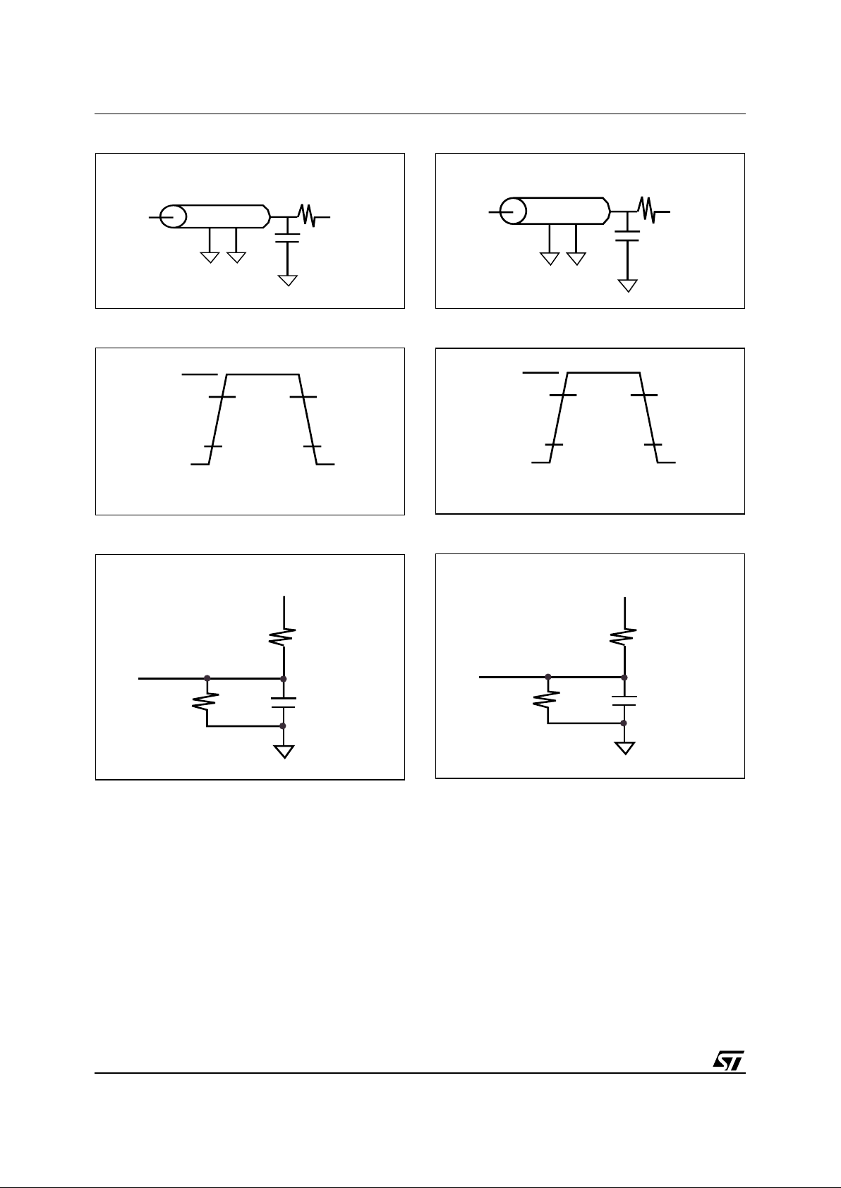
Figure 5. M7010R 2.5V AC Testing Load
Figure 6. M7010R 2.5V Input Waveform
Figure 7. M7010R 2.5V Output L oad Equiv.
Figure 8. M7010R 3.3V AC Testing Load
Figure 9. M7010R 3.3V Input Waveform
Figure 10. M7010R 3.3V Output Load Equiv.
C
L
VL= 1.25V
50ΩZ0 = 50Ω
D
OUT
AI04268
+2.5V
90%
10%
90%
10%
GND
AI04299
208Ω
192Ω
AI04266
5pF
Q
+2.5V
C
L
VL= 1.5V
50ΩZ0 = 50Ω
D
OUT
AI04269
+3.3V
90%
10%
90%
10%
GND
AI04298
158Ω
175Ω
AI04267
5pF
Q
+3.3V
Page 13
13/67
M7010R
Table 5. Capacitance
Note: Effective capacitance measured with power supply. Sampled only, not 100% tested.
1. Outputs deselected.
Table 6. DC Characteristi cs
Note: 1. Valid for Ambient OperatingTemperature:TA=0to70°C; VDD=1.8V.
Symbol Parameter Test Condition Min Max Unit
C
IN
Input Capacitance
V
IN
=0V
6pF
C
IO
(1)
Input / Output Capacitance
V
OUT
=0V
6pF
Symb Parameter
Test Condition
(1)
Min Max Unit
I
LI
Input Leakage Current
V
DDQ=VDDQ
(max)
0V ≤ V
IN
≤ V
DDQMAX
–10 +10 µA
I
LO
Output Leakage Current
V
DDQ=VDDQ
(max)
0V ≤ V
OUT
≤ V
DDQMAX
–10 +10 µA
I
DD1
1.8V Supply Current @ V
DDMAX
M7010R
I
OUT
= 0mA,
83MHz Search
1250 mA
M7010R
I
OUT
= 0mA,
66MHz Search
1000 mA
I
DD2
2.5V Supply Current @ V
DDMAX
M7010R
I
OUT
= 0mA,
83MHz Search
180 mA
M7010R
I
OUT
= 0mA,
66MHz Search
150 mA
I
DD3
3.3V Supply Current @ V
DDMAX
M7010R
I
OUT
= 0mA,
83MHz Search
300 mA
M7010R
I
OUT
= 0mA,
66MHz Search
240 mA
V
IL
Input Low Voltage –0.3 0.8 V
V
IH
Input High Voltage 2.0
V
DDQ
+0.3
V
V
OL
Output Low Voltage
V
DDQ=VDDQ
(min)
I
OL
=8mA
0.4 V
V
OH
Output High Voltage
V
DDQ=VDDQ
(min)
I
OH
= 8mA
2.4 V
Page 14
M7010R
14/67
Figure 11. AC Timing Waveforms with CLK2X
Cycle
1
Cycle
0
Cycle
2
Cycle
3
Cycle
4
Cycle
5
Cycle
7
Cycle
6
Cycle
8
Cycle
10
Cycle
12
Cycle
9
Cycle
11
CLK2X
Signal
Group 0
Signal
Group 2
Signal
Group 3
Signal
Group 4
Signal
Group 5
PHS_L
AI04265
Signal
Group 1
Signal Group 1: PHS_L, RST_L
Signal Group 1: DQ, CMD, CMDV
Signal Group 2: LHI, BHI, FULI
Signal Group 3: LHO, BHO, FULO, FULL
Signal Group 4: SADR, CE_L, OE_L, WE_L, ALE_L, SSF, SSV
Signal Group 5: DQ, ACK, EOT
tICSCH
tICHCH
tCKHOV
tCKHSV
tCKHSHZ
tCKHSLZ
tCKHOV
tIHCH
tISCH
tISCH
tISCH
tIHCH
tIHCH
tIHCH
tCKHDZ
tCKHDV
Page 15
15/67
M7010R
Table 7. AC Timing Parameters with CLK2X
Note: 1. Valid for Ambient OperatingTemperature:TA=0to70°C; VDD=1.8V.
2. Values are based on 50% signal levels.
3. BasedonanACloadofCL=50pF(seeFigure5,page12andFigure8,page12).
4. Unless otherwise noted, all values are based on AC load of CL = 50pF (see Figure 5, page 12 and Figure 8, page 12).
5. These parameters are sampled and not 100% tested.
Row Symbol
M7010R-066 M7010R-083
Unit
Description
(1)
Min Max Min Max
1
f
CLK
133 166 MHz CLK2X frequency
2
t
CLK
7.5 6.0 ns CLK2X period
3
t
CKHI
3.0 2.4 ns
CLK2X high pulse
(2)
4
t
CKLO
3.0 2.4 ns
CLK2X low pulse
(2)
5
t
ISCH
2.5 1.8 ns
Input Setup Timeto CLK2X rising edge
(2)
6
t
IHCH
0.6 0.6 ns
Input Hold Time to CLK2X rising edge
(2)
7
t
ICSCH
4.2 3.5 ns
Cascaded Input Setup Time to CLK2X rising edge
(2)
8
t
ICHCH
0.6 0.6 ns
Cascaded Input Hold Time to CLK2X rising edge
(2)
9
t
CKHOV
8.5 7.0 ns
Rising edge of CLK2X to LHO, FULO, BHO, FULL valid
(3)
10
t
CKHDV
9.0 7.5 ns
Rising edge of CLK2X to DQ valid
(4)
11
t
CKHDZ
8.5 7.0 ns
Rising edge of CLK2X to DQ high-Z
(5)
12
t
CKHSV
9.0 7.5 ns
Rising edge of CLK2X to SRAM Bus valid
(4)
13
t
CKHSHZ
6.5 6.0 ns
Rising edge of CLK2X to SRAM Bus high-Z
(4,5)
14
t
CKHSLZ
7.0 6.5 ns
Rising edge of CLK2X to SRAM Bus low-Z
(4,5)
Page 16

M7010R
16/67
OPERATION
Command Bus and DQ Bus
CMD[8:0] carries the com mand and its associated
parameter. DQ[67:0] is used for data transfer to,
and from the data base entries. The database entries are comprised of a data field and a mask field
which are organized as a data array and a mask
array. The DQ Bus carries t he SEARCH data during the SEARCH command as we ll as the address
and data during Pipelined I/O (P IO) READ/WRITE
operations, of the data array, mask array, and internal registers. The DQ Busalsocan carry the address information for the PIO accesses to the
SRAM.
Database Entry (Data Array a nd Mask Array)
Each database entry comprises a data field and a
mask field.The resultant value of t he entry is a logical AND of the corresponding data and mask bits
and can take logi c al values of '1,' '0' and 'X' (don’t
care), depending on t he v alue in the mask bi t. The
on-chip priority encoder selects the first matching
entry in the database which is nearest to location
0.
Arbitration Logic
When multiple (Silicon) Search Engines are cas caded to create large databas es , the data being
searched is presented to all Se arch proc es s ors simultaneously in thecascaded system.W hen more
than one device has duplicate entries, the arbitration logic on the Search Engine with the matching
entry whichis closest toaddress0 of the cascaded
database, will be selected to drive the SRAM Bus.
Pipeline and SRAM Control
Pipeline latency is added to give enough time t o
the arbi tration logic in a cascaded system to determine the index with the highest priority. T he pipeline logic adds latency to the SRAM access cycles
and the SSF and SSV signals to align t hem to the
host ASIC receiving the associated data. Refer to
Table 27, page 36 for details.
Full Logic
Bit[0] in each of the 68-bit entries has a special
purpose for the LEARN command (0 = empty, 1 =
full). When all thedata ent ries have Bit[0] set to '1,'
the database asserts the FULL flag, indicating that
all the Search Engines in the depth-cascaded array are full.
Connections Descri ption s
Master Clock (CLK2X). T he M7010R samples
all of the control and data signals on the pos itive
edge of CLK2X when PHS_L is low.
Phase (PHS_L). This signal runs at half the frequency of CLK2X and generates an internal clock
from CLK2X (see Figure 12, page 18).
Reset (RST_L). Driving RST low initializes the
device to a known state.
Command Bus (CMD[8:0]. [1:0] specifies the
command; [8:2] contains the comm and parameters. The descriptions of individual commands explains the details of t he parameters. The encod ing
of comman ds based on the [1:0] field are:
– 00: PIO READ
– 01 : PIO WRITE
– 10: SEARCH
– 11: LEARN
Command Valid (
CMDV). Qualifies the CMD bus
as follows:
– 0: No Command
– 1: Command
Address/Data Bus (
DQ[67:0]). Carries the READ
and WRITE address as well as the data during
register, data, and mask array operations. It carries the compare data during SEARCH operations. It also carries the SRAM address during
SRAM PIO accesses.
READ Acknowledge (ACK). Indicates that valid
data is available on the DQ Bus during register,
data, and mask array READ operations, or the
data is available on the SRAM data bus during
SRAM READ operations.
Note: ACK Signals require a pull-down resistor of
47Ω.
End of Transfer (EOT). Indicates the end of
burst t rans fer during READ or WRITE burst operations.
Note: EOT Signals re quire a pull-down resistor of
47 ohms.
SEARCH Successful Flag (SSF). When asserted, t his signal indicates t hat the device is the global winner in a SEARCH operation.
SEARCH Successful Flag Valid (SSV). When
asserted, this signal qualifies the SSF signal.
SRAM Address (SADR[21:0]). This bus con-
tains address lines to access off-chip SRAMs that
contain associative data. See Table 35, page 61
for the details of the generated SRA M address.
SRAM Chip Enable (CE_L). This is Chip Enable
control for external SRAMs. When more than one
device is cascaded, CE_L of all devices must be
connected.
SRAM WRITE Enable (WE_L). This is WRITE
Enable control for external SRAMs. When more
than one device is cascaded, WE_L of all devices
must be connected.
SRAM Output Enable (OE_L). This is Output
Enable control for external SR AM s . Only the last
device drives this signal (with the LRAM Bit set).
Page 17

17/67
M7010R
Address Latch Enable (ALE_L). When this sig-
nal is low, t he addresses on the SRA M address
bus havebeenvalidated.When more than one device is cascaded, the A LE_Lof all devices must be
connected.
Local Hit In (LHI[6:0]). These pins depth-cascade the device to form a larger table size. One
signal of th is bus is connected to the LHO[1] or
LHO[0] of each of the upstream devices in a block.
Connect all unused LHI pins to a logic '0. ' (For
more information, see DEPTH-CASCADING,
page 52.)
Local Hit Out (LHO[1:0]). LHO[1] and LHO[0]
are the same logical signal. LHO[1] or LHO[0] is
connected to one input of the LHI bus of up to four
downstream devices (in a block t hat cont ains up to
eight devices; for more information , s ee DEPTHCASCADING, page 52.)
Block Hit In (BHI[2:0]). Input s from the previous
BHO[2:0] are tied to the BHI[2:0] of the current device (see DEPTH-CASCADING, page 52). In a
four-block system, t he last block can cont ain only
seven devices because the ID c ode 11111 is used
for broadcast access.
Block Hit Out (BHO[2:0]). Outputs from the current de vic e are connected to the BHI[2:0] of the
next device (see DEPTH-CASCADING, page 52).
Full In (FUL I[6:0]). Each signal in this bus is connected to FULO[0] or FULO[1] of an upstream device to generate the FULL flag for the depth-
cascaded block. For more information, see
DEPTH-CASCADING, page 52 to Generate Full
for a Block Section.
Full Out (FULO[1:0]). FULO[1] and FULO[0] are
the same logical signal. One of these two signals
must be connected to the FULI of up to four downstream devices in a depth-cascaded table. Bit [0]
in the dat a array indicates if the entry is full (1) or
empty (0).This sign al is asserted if all of the bits in
the data array are '1s.' Refer to Depth-Cascading
to Generate a “FULL” State for a B lock , page 52.
Full Flag (FULL). When assert ed, this signal indicates that the table consisting of m any depthcascaded devices is full.
Device Identification (ID[4:0]). The binary-en-
coded device ID for a depth-cascaded system
starts at 00000 and goes up to 11110. 11111 is reserved for a special broadcast ad dres s that selects all cascad ed (silicon) Search Engines in t he
system. On a broadca st read-only, the device with
the LDEV Bit set to '1' responds.
Test Data In (TDI). This is the Test Access Port’s
Test Data In.
Test Clock (TCK). This is the Test Access Port’s
Test Clock.
Test Data Out (TDO). This is the Test Access
Port’s Test Data Out.
Test Mode Select (TMS). This is the Test Access Port’s Test Mode Select.
Test Reset (TRST_L). This is the Test Access
Page 18
M7010R
18/67
CLOCKS
The M7010R receives a Clock (CLK 2X ) signal and
Phase ( PHS_L) signal. The Phase (PHS_L) divides the CLK2X signal to generate the Internal
Clock (CLK), as shown in Figure 12. The CLK2X
and CLK signals are us ed for internal operations.
Registers
All the M7010R registers are 68 bits wide. The
M7010R contains 32 comparand storage registers, 16 global mask registers, 8 SEARCH-successful index registers, c ommand, information,
burst RE AD, burst WRITE, and next free address
registers. Table 8 provides a register overview of
all the registers. The registers a re ordered in ascending add re ss order.
Comparand Registers
The device contains t hirty-two 68-bit comparand
registers dynamically selected in every SEARCH
operation to store the comparand presented on
the DQ Bus. The LEARN command will also use
these registers when it is executed. The M7010R
stores the SEARCH command’s “Cycle A” comparand in the ev en-number register and the “Cycle
B” comparand in the odd-numbered register, as
shown in Figure 13, page 19.
Mask Registers
The device contains sixteen (8 pairs) 68-bit glo bal
mask registers dynamically s elect ed in every
SEARCH operation to select the SEARCH subfield (see Figure 14, page 19). The three-bit GMR
Index supplied on the CMD bus applies eight pairs
of global masks during the SEARCH and WRITE
operations, also shown in Figure 14.
Note: In 68-bit SEARCH and WRITE operations,
the host ASIC must program the even and odd
mask register with the same values, and the
M7010R uses even-numbered mask registers as
global masks.
Each mask b it in the global mask registers is used
during SEARCH and WR ITE operations. In
SEARCH operations, settingthe Mask Bit to '1' enables compares; setting the Mas k Bit to '0' disables compares (forced match) at the current bit
position. In WRITE operations to the data or mask
array, setting the Mask Bit to '1' enables WRITEs;
setting the Mask Bit to '0' disables WRITEs at the
corresponding bit position.
Figure 12. Clocks
Note: Any reference to “CLK Cycles” means 2 cycles of the signal, “CLK2X.”
1. “CLK” is an internal signal. The period for this clock is specified in Table 7, page 15.
Table 8. Register Overv iew
Address Abbreviation Type Name
0–31 COMP0–31 R
32 Comparand Registers. Stores comparands from the DQ Bus for
learning later.
32–47 MASKS RW 16 Global Mask Registers Array.
48–55 SSR0–7 R 8 SEARCH Successful Index Registers.
56 COMMAND RW Command Register.
57 INFO R Information Register.
58 RBURREG RW Burst READ Register.
59 WBURREG RW Burst WRITE Register.
60 NFA R Next Free Address Register.
61–63 ––Reserved
CLK2X
PHS_L
CLK
(1)
AI04274
Page 19
19/67
M7010R
Figure 13. Comparand Register Selection
During SEARCH and LEARN
Figure 14. Add ressing the Global Mask
Register(GMR) Array
SEARCH-Successful Registers
The device contains eight SEARCH-successful
registers (SSRs) to hold the index of the location
where a successful search occurred. Theformat of
each register is described in Table 9. The
SEARCH command specifies w hich SSR stores
the index of a specific SEARCH command in “Cycle B” of the SEARCH Instruction.
After the index location is specified, the host ASIC
can use this register to access t hat data array,
mask array, or external SRAM u sing the index as
part of the address (see SRAM ADDRESSING,
page 58). The device with a vali d bit set performs
a READ or WRITE operation. All other devices
suppress the operation.
Table 9. SEARCH-Successful R egister (SSR) Description
135 0
6868
1
0
32
54
7
6
30 31
0
15
1
Address
Index
AI04275
135 0
6868
1
0
32
54
7
6
9
8
11
10
13
12
15
14
0
1
6
7
2
5
4
3
Address
Index
AI04276
SEARCH and WRITE Command
Global Mask Selection
Field Range Initial Value Description
INDEX [13:0] X
Index. This is the address of the 68-bit entry where a successful search
occurs. The device updates this field if it has a successful search. In 136-bit,
the LSB is '0;' in a 272-bit configuration, the two LSBs are '00.' The index
updates if the device is either a local or global winner in a SEARCH
operation.
– [30:14] 0 Reserved.
VALID [31] 0
Valid. The device sets this bit to '1' if it is a global winner (first device
downstream with a hit) in a SEARCH operation, in a depth-cascaded
configuration.
– [67:32] 0 Reserved.
Page 20

M7010R
20/67
The Command Register
Table 10. Command Register Field Description s
Field Range Initial Value Description
SRST [0] 0
Software Reset. If '1,' this bit resets the device, with the same effect as the
hardware reset. Internally, it generates a reset pulse lasting for eight CLK
cycles. This bit automatically resets to a '0' during the reset cycle.
DEVE [1] 0
Device Enable. If '0,' it keeps the SRAM bus (SADR, WE_L, CE_L, OE_L,
and ALE_L), SSF, and SSV signals in a tri-state condition and forces the
cascade interface output signals LHO[1:0] and BHO[2:0] to '0.' It also keeps
the DQ Bus in Input mode. The purpose of this bit is to make sure that there
is no bus contention when the devices power-up in the system.
TLSZ [3:2] 01
Table Size. The host ASIC must program this field to configure the chips into
a table of a certain size. This field affects the pipeline latency of the SEARCH
and LEARN operations as well as the READ and WRITE accesses to the
SRAM (SADR[21:0], CE_L, OE_L, WE_L, ALE_L, SSV, SSF, and ACK).
Once programmed, the SEARCH latency stays constant.
Latency #
CLK Cycles
00: 1 device 4
01: 2-8 devices 5
10: 9-31
devices
6
11: Reserved
HLAT [6:4] 000
Latency of Hit Signals. This field adds latency to the SSF, SSV, and ACK
signals by the following number of CLK cycles during SEARCH and ACK
during an SRAM READ access.
000: 0 100: 4
001: 1 101: 5
010: 2 110: 6
011: 3 111: 7
LDEV [7] 0
Last device in the cascade. When set, this device is the last device in the
depth-cascaded table and is the default driver for the SSF and SSV signals.
In the event of a SEARCH failure, the device with this bit set drives the hit
signals as follows:
SSF = 0, SSV = 1
During non-search cycles, the device with this bit set drives the signals as
follows:
SSF = 0, SSV = 0
LRAM [8] 0
Last device on this SRAM Bus. When set, this device is the last device on
the SRAM bus in the depth-cascaded table and is the default driver for the
SADR, CE_L, WE_L, and ALE_L signals. In cycles where no M7010R
device (in a depth-cascaded table) drives these signals, the signals are
driven as follows:
SADR = 22’h3FFFFF, CE_L = 1, WE_L = 1, and ALE_L = 1.
OE_L is always driven by the device for which this bit is set.
Page 21

21/67
M7010R
CFG [16:9]
0000
0000
Database Configuration. The device is internally divided into four
quadrants of 8K x 68, each of which can be configured as 4K x 68, 2K x 136,
or 1K x 272 as follows:
00: 4K x 68
01: 2K x 136
10: 1K x 272
11: Reserved
Bits [10:9] apply to configuring the 1st quadrant in the address space.
Bits [12:11] apply to configuring the 2nd quadrant in the address space.
Bits [14:13] apply to configuring the 3rd quadrant in the address space.
Bits [16:15] apply to configuring the 4th quadrant in the address space.
[67:17] 0 Reserved.
Field Range Initial Value Description
Page 22

M7010R
22/67
SEARCH PROCEDURE FOR 32-BIT WIDE PREFIXES
The Global Mask Register is used f or 32-bit wide
data paths as follows:
Writing a '1' in t he Global Mask Register allows
data tobe written into the M7010R. A '0'in the Global Mask Register disallows data modification. Information is w ritten into the left half of the 68-bit
word Search Engine as long as space for 34 bi ts
of data is available and the n i nto t he right half of
the Search Engine. 32-bit data can be entered in
two cycles.
The first step is to write into two of the eight Global
Mask Registers with the patterns shown in Figure
15. Writing this data using Global Mask Register 1
allows the left half of the data array to be completely filled.
Figure 16 shows Bits 67 through 36 in the left section of the data array representing 32-bits of data.
Bits 35 and 34 shown separately can be defined
by the user for table management. In this application 34-bit ope ration occurs in each half-section of
the Data and Mask arrays of the Search Engine.
The left half is filled first, then the right. Not all locations have to be filled.
SEARCH operations areperforme d twice, once on
the left half and then on the right half. Note that a
'1' in the Global Mask regist er enables a compare
during a SEARCH operation and a '0' forces a
match condition regardless of the state of the data
bit.
The SEARCH throughput for 34-bit operations is
half of the 68-bit operations. A s earc h is performed
by using the Global Mask Register “0” for the left
half of the 68-bit, then another search ispe rform ed
using Global Mask Register 1 for the right half of
the 68-bit word. T he order is important, as the left
half has a higher priority than the right half.
For example, if a search on the left half produces
a matcha nd a search on the right halfalso produc-
es a match, then in that case, t he left half is a higher priority. So i f only one unique match exists in a
particular system, then a match on the left side
may alleviate the need to do a search on the right
half of the Data array.
Figure 15. Global Mask Register Patterns
Figure 16. St oring left half of a Data or Mask
Array
111 1000 0
000 0111 1
Register 0
Register 1
Bits 67 3433 0
AI04277
Bits 67 36 35 34 33 2 1 0
AI04278
Page 23

23/67
M7010R
The Information Register
Table 11. Information Registe r Field Descriptions
The READ Burst Address Register
(RBURREG)
These READ burst address r egister fields must be
programmed be fore burst READ (see Table 12).
The WRITE Burst Address Register
(WBURREG)
These WRI TE burst address register fields must
be program med b efore burst WRITE (see Table
13).
Table 12. READ Burst Register Description
Table 13. WRITE Burst Register Description
Field Range Initial Value Description
Revision [3:0] 0001
Revision Number. This is the current device revision number. Numbers start
from one and increment by one for each revision of the device.
Implemen-
tation
[6:4] 000 This is the M7010R implementation number.
Reserved [7] 0 Reserved.
Device ID [15:8] 00000001 This is the Device Identification Number.
MFID [31:16]
1101_1100_
0111_1111
Manufacturer ID. This field is the same as the manufacturer ID and
continuation bits.
[67:32] Reserved.
Field Range Initial Value Description
AADR [13:0] 0
Address. This is the starting address of the data array or mask array during
a burst READ operation. It automatically increments by 1 for each
successive read of the data array or mask array. Once the operation is
complete, the contents of this field must be reinitialized for the next
operation.
[18:14] Reserved.
BLEN [27:19] 0
Length of Burst Access. The device provides the capability to read from 4
up to 511 locations in a single burst. The BLEN decrements automatically.
Once the operation is complete, the contents of this field must be reinitialized
for the next operation.
[67:28] Reserved.
Field Range Initial Value Description
AADR [13:0] 0
Address. This is the starting address of the data array or mask array during
a burst WRITE operation. It automatically increments by 1 for each
successive write of the data array or mask array.It increments by 1 for each
successive read of the data array or mask array. Once the operation is
complete, the contents of this field must be reinitialized for the next
operation.
[18:14] Reserved.
BLEN [27:19] 0
Length of Burst Access. The device provides the capability to write from 4
up to 511 locations in a single burst. The BLEN decrements automatically.
Once the operation is complete, the contents of this field must be reinitialized
for the next operation.
[67:28] Reserved.
Page 24

M7010R
24/67
The NFA Register
Bit [0] of each 68-bit data entry is a special bit designated for use in the operation of the LEARN
command. In 68-bit configurations, the Bit[0] indicates whether a location is full (bit set to '1') or
empty (bit set to '0'). Every WRITE/LEARN command loads the address of f irst 68-bit location that
contains a “ 0” in the entry’s Bit[0]. This is stored in
the NFA register. If all th e bits in a device are set
to '1,' the M7010R asserts FULO[1: 0] to '1.'
In a 136-bit configuration, the LSB of this register
is always set to '0.' The host ASIC must set Bit 0
and Bit 68 in a 136-bit w ord to either '0' or '1' to indicate full/empty status for a 136-bit entry.
Note: Both Bits 0 and Bit 68 must be set t o '0' or
'1' (e.g., '10' or '01' settings are invalid).
Table 14. NFA Register
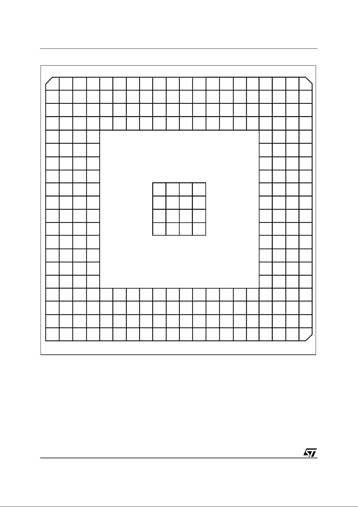
SEARCH ENGINE ARCHITECTURE
The M7010R c onsists of 16k x 68-bit storage cells
referred to as “data bits.” There is a m ask cellcorresponding to each data cell. Figure 17 shows the
three organizations of thedevice based on the value of CFG bits in the COMMAND register.
During a SEARCH operation, the SEARCH Data
Bit(S),DataArrayBit(D),MaskArrayBit(M)and
the Global Mask Bit (G) are used in the following
manner to generate a match at that bit pos ition
(see Table 15, page 25).
The entry with all matched bit positions results in a
successful se arc h in the M7010R. In order for a
successful SEARCH to make the device the l ocal
winner in the SEARCH operation, al l 68-bit positions within a device must generate a match for a
68-bit entry in 68-bi t-configured quadrants, or all
136-bit positions must generate a match for two
consecutive even and odd 68-bit entries in quadrants configured as 136 bits, or all 272-bit positions must generate a match for four consecutive
entries aligned to four entry-page boundaries of
68-bit entries in quadrants configured as 272 bits.
Anarbitrationmechani sm using a cascade bus determines the global w inning device am ong the local winning devices in a SEARCH cycle. The
global winning device drives the SRAM bus , SSV,
and The S SF signals. In the case of a SEARCH
failure, the device(s) with LDEV and LRAM bits set
drive the SRAM bus, S SF, and S SV signals.
The M7010R may be partitioned intoup to four (4)
quadrants of different widths (e.g., 34, 68, 136, or
272 bits), ev en within the same chip (see Application Notes AN1338 and AN1339). Figure18 shows
a sample configuration of different widths.
Data and Mask Addressing
Figure 19, page 26 s hows the M7010R data array
and mask array addressing procedure. T he data
array and mask array addresses differ only in one
bit in t he address cycle of the READ and WRITE
commands.
Address 67 - 14 13 - 0
60 Reserved Index
Page 25

25/67
M7010R
Figure 17. M7010R Database Configuration
Table 15. Bit Position M atch Figure 18. Multi-width Configuration Example
Data
Data
Data
Masks
Masks
Masks
16 K
CFG = 00000000
CFG = 01010101
CFG = 10101010
68
136
272
8 K
4 K
AI04264
G M S D Match
0xxx1
10xx1
11001
11010
11100
11111
4 K
4 K
2 K
1 K
68
68
136
272
CFG = 10010000
AI04244
Page 26

M7010R
26/67
Figure 19. M7010R Data and Mask Array Addr essing
CFG = 00000000
CF G = 101010 10
67 0
0
1
2
3
16383
271 0
3210
7654
16380 16381 16382 16383
68
CFG = 010 1010 1
135 0
10
32
54
76
16382 16383
(68-bit Configuration)
( 27 2- bi t c onf ig ur atio n)
(136-bit Configuration)
16 K
4K
8K
68 6868 68 6868
AI04263
Page 27

27/67
M7010R
COMMAND CODES AND PARAMETERS
A master device, such as an ASIC controller, issues commands to the M7010R using the CMDV
signal and the CMD Bus. The following subsections describe the functions of the commands.
Command Codes
The M7010R implements four basic commands
shown in Table 16. T he Command code must be
presented to CMD[1:0] while keeping the command valid (CMDV) signal high for two CLK2X cy-
cles. These two CLK2X cycles are designated as
“Cycle A” and “Cycle B.” The CMD[8:2]field passes the parameters of the command i n CLK2X Cycles A and B. The controller ASIC must align the
instructions with t he CLK2X si gnal.
Commands and Command Parameters
Table 17 lists the CMD bus fields that contain the
M7010R command parameters as well as the ir respective cycles.
Table 16. Command Codes
Table 17. Command Parameters
Note: The SRAM Address Bit SADR [19] in the command bit C6 will not be passed to the SRAM (see Table 28).
1. The 272-bit configuration does not support the LEARN Instruction.
CMD Code Command Description
00 READ
Reads one of the following: data array, mask array, device registers, or external
SRAM.
01 WRITE
Writes one of the following: data array, mask array, device registers, or external
SRAM.
10 SEARCH
Searches the data array for a desired pattern using the specified register from the
global mask register array and local mask associated with each data cell.
11 LEARN
The device has internal storage for up to 16 comparands that it can learn. The
device controller can insert these entries at the next free address (as specified by
the NFA register) using the LEARN Instruction.
Cmd Cyc 8 7 6 5 4 3 2 1 0
READ
A SADR[21] SADR[20] SADR[19] 0 0 0
0 = Single
1 = Burst
00
B0 0 0000
0 = Single
1 = Burst
00
WRITE
A SADR[21] SADR[20] SADR[19] GMR Index[2:0]
0 = Single
1 = Burst
01
B 0 0 0 GMR Index[2:0]
0 = Single
1 = Burst
01
SEARCH
A SADR[21] SADR[20] SADR[19] GMR Index[2:0]
68-bit or 136-bit: 0
272-bit:
1 in 1st Cycle
0 in 2nd Cycle
10
B Successful SEARCH Register Index[2:0] Comparand Register Index 1 0
LEARN
(1)
A SADR[21] SADR[20] SADR[19] Comparand Register Index 1 1
B0 0
Mode
0: 68-bit
1: 136-bit
Comparand Register Index 1 1
Page 28

M7010R
28/67
READ COMMAND
TheREADcanbeasinglereadofadataarray,a
mask array, an SRAM, or a register location
(CMD[2] = 0). It can be a burst READ (CMD[2] = 1)
using an internal auto-incrementing address register (RBURADR) of the data or mask array locations (see Table 18, page 30 and Table 19, page
30 for formats).
Asi ngle-lo ca tion READ operation takes six cycles,
as shown in Figure 20, page 29. The burst READ
adds two cycles for each successive read. The
SADR[21:19] bits su pplie d in the READ Instruction
Cycle A drives SADR[21:19] signals during the
PIO READ of anSRAM location.
The s ingle READ operation takes six CLK cycles,
in the following sequence:
– Cycle 1: The host ASIC applies the READ In-
struction on the CMD[1:0] (CMD[2] = 0), using
CMDV = 1, and th e DQ Bus supplies the address, as shown in Table 19, page 30 and Table
20, page 30. The host ASIC selects the device
for which ID[4:0] matches the DQ[25:21] lines. If
DQ[25:21] = 11111, the host ASIC selects the
M7010R with the L DEV Bit set. The host A SIC
also supplies SADR[21:19] on CMD[8:6] in Cycle A of the READ Instruction if the READ is directed to the external SRAM.
– Cycle 2: The host ASIC releases the DQ[67:0]
bus to a tri-state condition.
– Cycle 3: The hos t ASIC k eeps DQ[67:0] bus in
a tri-state condition.
– Cycle 4: The selected d ev ice starts to drive the
DQ[67:0] bus and drives the ACK signal from Z
to low.
– Cycle 5: The selected device drives t he READ
data from the addressed location on the
DQ[67:0] bus and drives the ACK signal high.
– Cycle 6: The selected device floats the
DQ[67:0] bus and drives the ACK signal low.
At the terminat ion of Cycle 6, the selected device
releases the ACK line to a tri-state condition. The
READ Instruction is complete, and a new operation can begin.
Theb urst READ operation lasts 4 + 2n CLK-cycles
(where “n” stands for the number of accesses in
the burst specified by theBLE N field of the RBURREG) in the sequence s hown in Figure 21, page
29. This operation assumes that the host ASIC
has programmed the RBURREG with the starting
address (ADDR) and the length of transfer (BLEN)
before initiating the burst READ command.
– Cycle 1: The host ASIC applies the READ In-
struction on the CMD[1:0] (CMD[2] = 1), using
CMDV=1 and the addres s supplied on the DQ
Bus, as shown in Table 21, page 31. The host
ASIC selectsthe device forwhich ID[4:0] matches the DQ[25:21] lines. If D Q[25:21] = 11111,
the host AS IC selects the M7010R with the
LDEV Bit set.
– Cycl e 2: The host ASIC floats DQ[67:0] to a tri-
state condition.
– Cycle 3: The hos t ASIC k eeps DQ[67:0] bus in
a tri-state condition.
– Cycle 4: The selected d ev ice starts to drive the
DQ[67:0] bus and drives ACK, and EOT from Z
to low.
– Cycle 5: The selected device drives t he READ
data from the addressed location on the
DQ[67:0] bus and drives the ACK signal high.
Note: Cycles four and five repeat for each additional access until all the accesses specified in
the burst length (BLEN) field of RBURREG are
complete. On t he last transfer, the M7010R
drives the EOT signal high.
– Cycle (4 + 2n): The selected device drives the
DQ[67:0] to 3-state condition and drives t he
ACK and the EOT signals low.
At the te rmin ation of Cycle 4 + 2n, the selected device floats the ACK line to 3-state condition. The
burst READ Instruction is comp lete, and a new operation can begin (see Table 21, page 31 for burst
READ address formats).
Page 29

29/67
M7010R
Figure 20. Single Location READ Cycle Timing
Figure 21. Burst READ of the Data and Mask Arrays (BLEN = 4)
Cycle 1 Cycle 2 Cycle 3 Cycle 4 Cycle 5 Cycle 6
CLK2X
CMDV
CMD[1:0]
ACK
DQ
PHS_L
AI04282
Read
CMD[8:2]
A B
Address
X
Data
Cycle
1
Cycle
2
Cycle
3
Cycle
4
Cycle
5
Cycle
7
Cycle
6
Cycle
8
Cycle
10
Cycle
11
Cycle
12
Cycle
9
CLK2X
CMDV
CMD[1:0]
ACK
EOT
DQ
PHS_L
AI04283
Read
CMD[8:2]
A B
Address
FF
Data0
FF
Data1
FF
Data2
FF
Data3
Page 30

M7010R
30/67
Table 18. READ Command Parameters
Table 19. Data and Mask Array, SRAM READ Address Format
Note: 1. “|” stands for logicalOR operation,and “{}”stands for concatenation operator.
Table 20. READ Address Format for Internal Registers
CMD Parameter
CMD[2]
Read Command Description
0 Single Read
Reads a single location of the data array, mask array,external SRAM,
or device registers. All access information is applied on the DQ Bus.
1 Burst Read
Reads a block of locations from the data array or mask array as a
burst.
The internal register (RBURADR) specifies the starting address and
the length of the data transfer from the data array or mask array,and it
auto-increments the address for each access.
All other access information is applied on the DQ Bus.
Note: The device registers and external SRAM can only be read in
single-read mode.
DQ
[67:30]
DQ
[29]
DQ
[28:26]
DQ
[25:21]DQ[20:19]DQ[18:14]
DQ
[13:0]
Reserved
0: Direct
1: Indirect
SuccessfulSEARCH
Register Index
(Applicable if DQ[29]
is indirect)
ID
00: Data
Array
Reserved
If DQ[29] is '0,' this field carries
address of data array location.
If DQ[29] is '1,' the successful
SEARCH Register specified on
DQ[28:26] supplies the address
of the data array location:
{SSR[13:2], SSR[1] | DQ[1],
SSR[0] | DQ[0]}
(1)
Reserved
0: Direct
1: Indirect
SuccessfulSEARCH
Register Index
(Applicable if DQ[29]
is indirect)
ID
01: Mask
Array
Reserved
If DQ[29] is '0,' this field carries
address of mask array location.
If DQ[29] is '1,' the successful
SEARCH Register specified on
DQ[28:26] supplies the address
of the mask array location:
{SSR[13:2], SSR[1] | DQ[1],
SSR[0] | DQ[0]}
(1)
Reserved
0: Direct
1: Indirect
SuccessfulSEARCH
Register Index
(Applicable if DQ[29]
is indirect)
ID
10:
External
SRAM
Reserved
If DQ[29] is '0,' this field carries
address of SRAM location.
If DQ[29] is '1,' the successful
SEARCH Register specified on
DQ[28:26] supplies the address
of the SRAM location.
DQ[67:26] DQ[25:21] DQ[20:19] DQ[18:6] DQ[5:0]
Reserved ID 11: Register Reserved Register Address
Page 31

31/67
M7010R
Table 21. READ Address Format for Data and Mask Arrays
WRITE COMMAND
TheWRITEcanbeasinglewriteofadataarray,
mask array, register, or external SRAM location
(CMD[2] = 0). It can also be a burst WRITE
(CMD[2] = 1) using an internal auto-increm enting
address register (WBURADR) of the data array or
mask array locations (see Table 23, page 33 for
format). A single-location WRITE is a three-cycle
operation, shown in Figure 22, page 32. The burst
WRITE adds one extra cycle for each successive
location write.
The WRITE operation sequence is as f oll ows :
– Cycle 1A: The host ASIC applies the WRITEIn-
structiontoCMD[1:0](CMD[2]=0),usingCMDV=1 and the address supplied on the DQ Bus,
as shown in Table 22, page 33. The hos t ASIC
also supplies the in dex to the global mask register (GMR) to mask the WRITE to the data arrayormaskarraylocationinCMD[5:3].For
SRAM writes, the host ASIC must supply
SADR[21:19] on CMD[8:6].
– Cycle 1 B: The host AS IC continues to apply the
WRITE Instruction to CMD[1:0] (CMD[ 2] = 0)
using CMDV = 1 and the addres s supplied on
the DQ B us. The host ASIC continues to supply
the GMR Index to mask the WRITE to t he data
or mask array locations in CMD[5:3]. The ho st
ASIC selects the device where ID[4:0] ma tches
the DQ[2 5:21] = 11111.
– Cycle 2: The host ASIC drives the DQ[67:0]
with the data to be written to the data array,
mask array, ex te rnal SRAM, or register location
of the selected device.
– Cycle 3: Idle cycle. At the termination of this cy-
cle, another operation can begin.
The burst WRITE operation lasts for (n + 2) CLK
cycles,where“n”signifies the number of accesses
in the burst as specified in the BLEN field of the
WBURREG register (see Figure 23 , page 32).
This operation assumes that the host ASIC has
programmed the WBURREG with t he starting address (ADDR) and the length of trans fer (BLEN)
before initiating t he burst WRI TE command (see
Table 24, page 33 for format). The s equence is as
follows:
– Cycle 1A: The host ASIC applies the WRITE In-
struction on the CMD[1:0] (CMD[2] = 1), using
CMDV = 1 and the address supplied on the DQ
Bus, as shown in Table 23, page 33. The host
ASIC also supplies the index to the global mask
register to mask the WRITE to the data or mask
array locations in CMD[5:3].
– Cycle 1B: Thehost ASIC continues to apply the
WRITE Instruction to CMD[1:0] (CMD[ 2] = 0)
using CMDV = 1 and the addres s supplied on
the DQ B us. The host ASIC continues to supply
the GMR Index to mask the WRITE to t he data
or mask array locations in CMD[5:3]. The host
ASIC selects the device where ID[4:0] ma tches
the DQ[2 5:21] = 11111.
– Cycle 2: The host ASIC drives the DQ[67:0]
withthedatatobewrittentothedataarrayor
mask array location of the selected device. The
host ASIC writes the data on the D Q[67:0] bus
only to the subfield that has the corresponding
mask bit set to '1' in the global m as k regi ster
specified by the index CM D[5:3] and supplied in
Cycle 1.
– Cycles 3 to n + 1: The ho st ASIC drives
DQ[67:0] with the data to be written to the next
data array or mask array location (addressed by
the auto-increment AADR field of the WBURREG register) of the selected device.
The host ASI C writes the data on the DQ[67:0]
bus only tothe sub field that has the corresponding mask bit set to '1'in th e global mask register
specified by the index CM D[5:3] and supplied in
Cycle 1. The M7010R drives the EOT signal low
from Cycle 3 to Cycle n; the M7010R drives the
EOTsignalhighinCyclen+1(nisspecifiedin
the BLEN field of the WBURREG).
– Cycle n + 2: TheM7010R drives the EOT signal
low. At the t ermination of the Cycle n + 2, the
M7010R floats the EOT signal to a 3-state, and
a new instruction can begin.
DQ[67:26] DQ[25:21] DQ[20:19] DQ[18:14] DQ[13:0]
Reserved ID 00: Data Array Reserved
Do not care. These 14 bits come from the
internal register (RBURADR) which
increments for each access.
Reserved ID 01: Mask Array Reserved
Do not care. These 14 bits come from the
internal register (RBURADR) which
increments for each access.
Page 32

M7010R
32/67
Figure 22. Single Location WRITE Cycle Timing
Figure 23. Burst WRITE of the Data and Mask Arrays (BLEN = 4)
Cycle 1 Cycle 2 Cycle 3 Cycle 4Cycle 0
CLK2X
CMDV
CMD[1:0]
DQ
PHS_L
AI04284
Write
CMD[8:2]
A B
Address
Data
X
Cycle1Cycle2Cycle3Cycle4Cycle5Cycle
6
CLK2X
CMDV
CMD[1:0]
EOT
DQ
PHS_L
AI04285
Write
CMD[8:2]
A B
Address
Data0
Data1
Data2
Data3
X
Page 33

33/67
M7010R
Table 22. (Single) WRITE Address Format for Data and Mask Arrays or S RAM
Note: 1. “|” stands for logicalOR operation,and “{}”stands for concatenation operator.
Table 23. WRITE Address Format for Internal Registers
Table 24. WRITE Address Format for Data and Mask Array (Burst WRITE)
DQ
[67:30]
DQ
[29]
DQ
[28:26]
DQ
[25:21]DQ[20:19]
DQ
[18:14]
DQ
[13:0]
Reserved
0: Direct
1: Indirect
Successful
SEARCH
Register Index
(Applicable if
DQ[29] is
indirect)
ID
00: Data
Array
Reserved
If DQ[29] is '0,' this field carries the
address of the data array location.
If DQ[29] is '1,' the SSR specified on
DQ[28:26] is used to generate the
address of the data array location:
{SSR[13:2], SSR[1] | DQ[1], SSR[0]
| DQ[0]}.
(1)
Reserved
0: Direct
1: Indirect
Successful
SEARCH
Register Index
(Applicable if
DQ[29] is
indirect)
ID
01: Mask
Array
Reserved
If DQ[29] is '0,' this field carries
address of the mask array location.
If DQ[29] is '1,' the SSR specified on
DQ[28:26] is used to generate the
address of the data array location:
{SSR[13:2], SSR[1] | DQ[1], SSR[0]
| DQ[0]}.
(1)
Reserved
0: Direct
1: Indirect
Successful
SEARCH
Register Index
(Applicable if
DQ[29] is
indirect)
ID
10: External
SRAM
Reserved
If DQ[29] is '0,' this field carries
address of the data SRAM location.
If DQ[29] is '1,' the SSR specified on
DQ[28:26] is used to generate the
address of the data array location:
{SSR[13:2], SSR[1] | DQ[1], SSR[0]
| DQ[0]}.
(1)
DQ[67:26] DQ[25:21] DQ[20:19] DQ[18:6] DQ[5:0]
Reserved ID 11: Register Reserved Register address
DQ
[67:26]
DQ
[25:21]
DQ
[20:19]
DQ
[18:14]
DQ
[13:0]
Reserved ID 00: Data array Reserved
Don’t care. These 14 bits come from the
internal register (WBURADR), which
increments with each access.
Reserved ID 01: Mask array Reserved
Don’t care. These 14 bits come from the
internal register (WBURADR), which
increments with each access.
Page 34

M7010R
34/67
SEARCH COMMAND
The M7010R Search Engine can be configured in
three ways:
1. 68-bit
2. 136-bit
3. 272-bit
4. Mixed-sized SEARCHES on tables configured with different widths
68-bit Configuration
Figure 25, page 35 shows the tim ing diagram f or a
SEARCH operation in the 68-bit-configured table
(one device only). This illustration assumes that
the hos t ASIC has programmed TLSZ to '00,'
HLAT to '000,' LRAM to '1,' and LDEV to '1' in the
command register. The hardware diagram for this
search subsystem is shown in Figure 24.
– Cycle A: ThehostASICdrivesCMDVhighand
applies the SEARCH command c ode (10) on
CMD[1:0]. CMD[5:3] must be driven by the index to the global mask register pair for use in
the SEARCH operation. CMD[8:6] signals must
be driven by the same bits that will be driven on
SADR[21:19] by this dev ice if it has a hit.
DQ[67:0] must be driven with the data to be
compared. CMD[2] signal must be driven to logic '0.'
– Cycle B: The host ASIC continues to drive
CMDV high and to apply the SEARCH command (10) on CMD[1:0].C MD[5: 2] must be driven by the index of the comparand register pair
forstoring the 136-bit wordpresented on the DQ
Bus du r ing Cycles A and B. CMD[8:6] s ignals
must be driven with the index of the SSR that
will be used for s t oring the address of t he
matching entry and the hit flag. The DQ[67:0]
continues to carry the 68-bit data to be compared.
Note: In the 68-bit configuration, the host ASIC
must supply the same data on DQ[67:0] du ring
cycles A and B. The even and odd GMR pairs
selected for the compare must be programmed
with the same value.
The SEARCH command is a pipelined operation
and executes a SEARCH at half their rate of frequency of CLK2X for 68-bit searches in x68-configured tab les. The latency of SADR, CE_L,
ALE_L, WE_L, SSV, and SSF from 68-bit
SEARCH Command cycle (= two CLK2X cycles)
is shown in Table 27, page 36.
The timing diagram for all SRAM interface s ignal s,
SSV, and SSF shift t o the right for different values
of TLSZ, as s pec if ied in Table 25, page 36 and Table 26, page 36.
In addition, SS V and SSF shift to the right for different values of HLAT, as specified in Table 26,
page 36.
68-bit Configuration with LDEV = 1. The de-
vice is configured to be the last in the depth-cascaded tableby setting LDEV to '1'in the Command
Register. The device with LDEV set to '1' drives
the SSF and SS V signals in cycles when all upstream devices do not drive these signals. The
M7010R with itsLDEV Bit set drives S S F and SSV
during a search with a miss or with non-search
commands (see the LDEV Bit definition in Table
10, page 20).
68-bit Configuration with LRAM = 1. Setting
LRAM to '1' i n the Command Register configures
the device tobe the last on the SRAM Bus. Ina cycle where the upstream device does not drive the
SRAM Bus, the last device of the SRAM Bus (with
LRAM = 1) drives t he bus (SADR, CE_L, WE_L,
ALE_L) when they are active. When set to '1,' the
LRAM B it sets the default driverfor the SRAM control signals (SADR, CE_L, WE_L, and ALE_L).
Figure 24. Hardware Diagram for a Table with a Single Device (68-bit Operation)
DQ[67:0]
CMDV, CMD[8:0]
SSF, SSV
SRAM
LHO[1]
BHI[2:0]
BHI[2:0]
LHI
3210
M7010R
LHO[0]
654
AI07040
Page 35

35/67
M7010R
Figure 25. 68-Bit Configuration SEARCH Timing Diagram (One Device)
Cycle
1
Cycle
2
Cycle
3
Cycle
4
Cycle
5
Cycle
7
Cycle
6
Cycle
8
Cycle
10
Cycle
9
CLK2X
CMDV
CMD[1:0]
ALE_L, CE_L
WE_L
OE_L
SADR[21:0]
SSV
SSF
CMD[8:2]
PHS_L
AI04286
A
B
A
B
A
B
A
B
DQ
D1
D2
D3
A1
1
1
11
1111
11
0
0
0
0
0
0
0
0
0
1
0
0
0
A3
D4
01
01
01 01
Hit MissHit Miss
CFG = 00000000, HLAT = 000, TLSZ = 00, LRAM = 1, LDEV = 1
Search1
Search2
Search3
Search4
Page 36

M7010R
36/67
Table 25. Right-Shiftof 68-bitSignals for TLSZ
Values
Table26. Shiftof SSF and SSV from SADR (for
different HLAT Values)
Table 27. Latency of SE ARCH from Instruction to SRAM Access Cycle (68-bit Mode)
TLSZ Number of CLK Cycles
00 0
01 1
10 2
HLAT Number of CLK Cycles
000 0
001 1
010 2
011 3
100 4
101 5
110 6
111 7
# of devices Max Table Size Latency in CLK Cycles
1 (TLSZ = 00) 16K x 68-bit 4
2–8 (TLSZ = 01) 128K x 68-bit 5
9–31 (TLSZ = 10) 496K x 68-bit 6
Page 37

37/67
M7010R
68-bit Logical SEARCH
The logical, 68-bit SEARCH operation is shown in
Figure 26. The entire table of 6 8-bit entries is compared t o a 68-bit word K (pres ent ed on the DQ Bus
in both Cycles A and B of the com mand) using the
GMR and the local mask bits. The effective GMR
is the 68-bit word specified by the identical value
in both even and odd GMR pairs selected by the
GMR Index in the command’s Cycle A. The 68-bit
word K (presented on the DQ Bus in both Cycles
A and B of the command) is also stored in both
even and odd comparand register pairs s elected
by the Comparan d R egister Index in the command’s Cycle B . In a x68 configuration, only the
even comparand register can subsequently be
used by the LEARN command. The word K (presented on the DQ Bus in both Cycles A and B of
the command) is compared with each entry in the
table, starting at location “0.” The first matching
entry’s location, address “L,” is the winning ad-
dress that is driven as part of the SRAM address
on the SADR[21:0] lines.
Figure 26. x68 Table with One Device
Comparand Register (even)
Comparand Register (odd)
67
0
K
CFG = 00000000
0
1
2
3
16383
(68- bi t Configuration)
Location
address
L
K
67
0
K
GMR
67
0
AI07041
(First matching entry)
Page 38

M7010R
38/67
136-bit Configurati on
Figure 28, page 39 shows the timing diagram for
the SEARCH operation in the 136-bit table(CFG =
01010101) consisting ofa single device forone set
of parameters: TLSZ = 00 , HLAT = 001, LRAM =
1, and LDEV = 1. The hardware diagram for t he
search subsystem is shown in Figure 27.
The f ollowing is the operation sequence for a single, 136-bit SEARCH command.
– Cycle A: The hos t ASIC drives the CMDV hi gh
and applies the SEARCH command code (10)
to CMD[1:0] signals. CMD[5:3] signals must be
driven with the index to the GMR pair for use in
this SEARCH opera tion. CMD[8:6] s ignal s must
be driven with the same bits that will b e driven
on SADR[21:19] by this device if it has a hit.
DQ[67:0] mus t be driven with the 68-bit data
([135:68]) to be compared against all even locations. The CMD[2] signal must be driven to logic
'0.'
– Cycle B: The host A SIC continues to drive the
CMDV high and appl ies SEARCH command
code (10) on CMD[1:0]. CMD[5:2] must be driven by the index to the comparand register pair
forstoring the 136-bit wordpresented on the DQ
Bus du r ing Cycles A and B. CMD[8:6] s ignals
must be driven by the index of t he SSR that will
be used for storing the address of the matching
entry and hit flag. The DQ[67:0] is driven with
68-bit data ([67 :0]), compared to all odd locations.
Note: For 136-bit searches, the host ASIC must
supply two distinct, 68-bit data words on
DQ[67:0] during Cycles A and B. The evennumbered GMR of the pair specified by the
GMR Index is used for masking the word in Cy cle A. Theodd-numbered GMR of the pairspecified by the GMR Index is used for masking the
word in Cycle B .
The SEARCH command is a pipelined operation
that executes searches at half the rate of the frequency of CLK2X for 136-bit searches in x136-bitconfigured tables. The latency of SADR, CE_L,
ALE_L, WE_L, SSV, and SSF from the 136-bit
SEARCH command cycle (two CLK2X cycles) is
shown in Table 30, page 40.
The timing diagram for all SRAM interface s ignal s,
SSV, and SSF shift t o the right for different values
of TLSZ, as specified in Table 28, page 40.
In addition, SS V and SSF shift to the right for different values of HLAT, as specified in Table 29,
page 40.
The result of the SEARCH op eration appears as
an SRA M READ Cycle with a pipelined latency. It
is specified as shown in Table 3 0, page 40.
Figure 27. Hardware Diagram for a Table with One Device (136-bit Operation)
DQ[67:0]
CMDV, CMD[8:0]
SSF, SSV
SRAM
LHO[1]
BHI[2:0]
BHI[2:0]
LHI
3210
M7010R
LHO[0]
654
AI07040
Page 39

39/67
M7010R
Figure 28. 136-Bit Configuration SEARCH Timing Diagram (One Device)
Cycle
1
Cycle
2
Cycle
3
Cycle
4
Cycle
5
Cycle
7
Cycle
6
Cycle
8
Cycle
10
Cycle
9
CLK2X
CMDV
CMD[1:0]
ALE_L, CE_L
WE_L
OE_L
SADR[21:0]
SSV
SSF
CMD[8:2]
PHS_L
AI04287
A
B
A
B
A
B
A
B
A
B
A
B
A
B
A
B
DQ
D1
D2
D3
A1
1
1
11
1111
11
0
0
0
0
0
0
0
0
0
1
0
0
0
A3
D4
01
01
01 01
Hit MissHit Miss
CFG = 01010101, HLAT = 001, TLSZ = 00, LRAM = 1, LDEV = 1
Search1
Search2
Search3
Search4
Page 40

M7010R
40/67
Table 28. Right-Shift of 136-b it Signals for
TLSZ Values
Table29. Shiftof SSF and SSV from SADR (for
different HLAT values)
Table 30. Latency of SE ARCH from Instruction to SRAM Access Cycle (136-bit Mode)
TLSZ Number of CLK Cycles
00 0
01 1
10 2
HLAT Number of CLK Cycles
000 0
001 1
010 2
011 3
100 4
101 5
110 6
111 7
# of devices Max Table Size Latency in CLK Cycles
1 (TLSZ = 00) 8K x 136-bit 4
2–8 (TLSZ = 01) 64K x 136-bit 5
9–31 (TLSZ = 10) 248K x 136-bit 6
Page 41

41/67
M7010R
136-bit Logical SEARCH
The logical, 136-bit SEARCH operation is shown
in Figure 29. The entire table of 136-bit entries is
compared to a 136-bit word K (presented on the
DQ Bus in both Cycles A and B of the command)
using the GMR and the local mask bits. The GMR
is the 136-bit word specified by the even and odd
global mask pair s elect ed by GMR Index in t he
command’s Cycle A. The 136-bit word K (presented on the DQ Bus in both C y cles A and B of the
command) is also stored in both even and odd
comparand register pairs selected by the Comparand Register Index in the command’s Cycle B.
The two comparand registers can su bs equent ly
be used by the LE ARN c ommand with the even-
numbered comparand register stored in an evennumbered location, and the odd-numbered comparand register stored in an adjacent, odd-numbered loc ation. The word K (presented on the DQ
BusinCyclesAandBofthecommand)iscompared with each ent ry in the table s tarting at location “0.” Th e first matching entry’s location,
address “L,” is the winning address that is driven
as part of the SRAM address on the SADR[21:0]
lines.
Note: The matching address is always goi ng to be
an even-numbered addres s for a 136-bit
SEARCH.
Figure 29. x136 Table with One Device
Comparand Register (even)
Comparand Register (odd)
67
0
A
CFG = 01010101
0
2
4
6
16382
(136- bi t Configuration)
Location
address
L
B
135
0
KA B
GMR Even Odd
135
0
AI07042
(First matching entry)
Page 42

M7010R
42/67
272-bit Configurati on
Figure 31, page 43 shows the timing diagrams for
a SEARCH operation in the 272-bit-configured table (CFG = 10101010) consisting of a single device for one set of parameters: TLSZ = 00, HLAT
= 001, LRAM = 1, and LDEV = 1. The hardware diagram for this search subsystem is shown in Figure 30.
– Cycle A: The hos t ASIC drives the CMDV hi gh
and applies the SEARCH command code (10)
to CMD[1:0] signals. CMD[5:3] signals must be
driven wi th the index to the GM R pair for bits
[271:136] of the data being searched. DQ[67:0]
must be driven with the 68-bit data ([271:204])
to becom pared to all locations “0” in t he four 68bits-word page. The CMD[2] signal mus t be
driventologic'1.'
Note: CMD[2 ] = 1 signals that the search is a
x272-bit search. CMD[8:3] is ignored.
– Cycle B: The hos t ASIC continues t o drive
CMDV high and continues t o apply SEARCH
command code (10) on CMD[1:0]. T he
DQ[67:0] is driven with 68-bit data ([203:136]) to
be compared to all locations “1” in the 68-bitsword page.
– Cycle C: The hos t ASIC drives the CMDV hi gh
and applies the SEARCH command code (10)
to CMD[1:0] signals. CMD[5:3] signals must be
driven wi th the index to the GM R pair for bits
[135:0] of the data bein g s earc hed. CMD[8:6]
signals must be driven with the bits that will be
driven on SADR[21:19] by this device if it has a
hit. DQ[67:0] must be driven with the 68-bit data
([135:68]) to be compared to all locations “2” in
the four 68-bits-word page. The CMD[2] signal
must be driven to logic '0.'
– Cycle D: The host ASIC continues to drive
CMDV high and appl ies SEARCH command
code (10) on CMD[1:0]. CMD[8:6] s ignals must
be driven with the index of the S S R that will be
used for storing the address of the matchi ng entry and hit flag (see Table 9, page 19 for a description of SSR[0:7]). The DQ[67:0] is driven
with th e 68-bit data ([ 67: 0]) to be compared toall
locations “3” in the four 68-bits-word page.
CMD[5:2] is ignored because the LEARN Instruction is not supported for x272 tables.
Note: For 272-bit searches, the host ASIC must
supply four distinct 68-bit data words on
DQ[67:0] during Cycles A, B, C, and D. The
GMR Index in Cycle A selects a pair of GMRs
that apply to DQ data in Cycles A and B. T he
GMR Index in Cycle C selects a pair of GMRs
that apply to DQ data in C y c les C and D.
The SEARCH command is a pipelined operation
that executes searches at one-fourth t he rate of
the frequency of CLK2X for 272-b it searches in
x272-bit-configured tables. The latency of SADR,
CE_L, ALE_L, WE_L, SSV, and SSF from the
272-bit SEARCH command (measured in CLK cycles) from the CLK2X cycle that contains the C
and D cycles is shown in Table 33, page 44.
The timing diagram for all SRAM interface s ignal s,
SSV, and SSF shift t o the right for different values
of TLSZ, as specified in Table 31, page 44.
In addition, SS V and SSF shift to the right for different values of HLAT, as specified in Table 32,
page 44.
In t he 272-bit configuration, SEA RCH takes two
CLK cycles. The result of the SEARCH operation
appears asan SRAM READ Cycle witha pipelined
latency measured from the second cycle of the
command, as specified in Table 33, page 44.
Figure 30. Hardware Diagram for a Table with One Device (272-bit Operation)
DQ[67:0]
CMDV, CMD[8:0]
SSF, SSV
SRAM
LHO[1]
BHI[2:0]
BHI[2:0]
LHI
3210
M7010R
LHO[0]
654
AI07040
Page 43

43/67
M7010R
Figure 31. 272-Bit Configuration SEARCH Timing Diagram (One Device)
Cycle
1
Cycle
2
Cycle
3
Cycle
4
Cycle
5
Cycle
7
Cycle
6
Cycle
8
Cycle
10
Cycle
9
CLK2X
CMDV
CMD[1:0]
CMD[2]
ALE_L, CE_L
WE_L
OE_L
SADR[21:0]
SSV
SSF
CMD[8:2]
PHS_L
AI04288
A
B
A
B
A
B
A
B
A
B
A
B
A
B
A
B
DQ
D1
D2
1
1
1
11
1
0
0
0
0
0
0
1
0
1
0
0
0
ABCD
01
01
Hit Miss
CFG = 10101010, HLAT = 001, TLSZ = 00, LRAM = 1, LDEV = 1
Search1
Search2
A1
Page 44

M7010R
44/67
Table 31. Right-Shift of 272-b it Signals for
TLSZ Values
Table32. Shiftof SSF and SSV from SADR (for
different HLAT Values)
Table 33. Latency of SE ARCH from Instruction to SRAM Access Cycle (272-bit Mode)
TLSZ Number of CLK Cycles
00 0
01 1
10 2
HLAT Number of CLK Cycles
000 0
001 1
010 2
011 3
100 4
101 5
110 6
111 7
# of devices Max Table Size Latency in CLK Cycles
1 (TLSZ = 00) 4K x 272-bit 4
2–8 (TLSZ = 01) 32K x 272-bit 5
9–31 (TLSZ = 10) 124K x 272-bit 6
Page 45

45/67
M7010R
272-bit Logical SEARCH
The logical 272-bit SEARCH operation is shown in
Figure 32. The entire table of 272-bit entries is
compared to a 272-bit word K (presented on the
DQ Bus in both Cycles A, B, C, and D of the command) using the GMR and the local mask bits. The
GMR is the 272-bit word specified by the two pairs
of GMRs selected by G MR Ind ex es in the command’s Cycles A and C. T he 272-bit word K (presented on the DQ Bus in Cycles A, B, C, and D of
the command) is compared with each entry in the
tablestartingatlocation“0.”
The first matching ent ry’ s location, address “L,” is
the winning address that is driven as part of the
SRAM addres s on the SADR[21:0] lines.
Note: The matching address is always goi ng to be
location “0” in a four-entry page for a 272-bit
SEARCH (two LSBs of the matching index will be
“00”).
Figure 32. x272 Table with One Device
CFG = 10101010
0
4
8
12
16380
(272- bi t Configuration)
Location
address
L
271
0
KA B C D
GMR 0 1
23
271
0
AI07044
(First matching entry)
Page 46

M7010R
46/67
Mixed-sized Searches on Tables Configured with Different Width Using an M7010R Device
This subsection will c ov er mixed searches (x68,
x136, and x272) with tables of different widths
(x68, x136, and x272). The sample operation
shown isfor a single device w it h CFG = 10010000,
containing three tables of x68, x136, and x 272
widths. The operation can be gene ralized to a
block of 8 to 31 devices using four blocks; the timing and the pipeline operation is the same as described previously for fixed searches on a table of
one-width-size.
Figure 34, page 47 shows three sequential
searches; first, a 68-bit SEARCH on a table configured as x68, then a 136-bit SEARCH on a table
configured as x136, and finally a 272-bit SEA RCH
on the table configured as x272. Each results in a
hit.
Note: The DQ[67:66] will be “00”in each of the two
A and B Cycles of the x68-bit SEARCH (Search1).
DQ[67:66] is “01” in each of the A and B Cycles of
the x136-bit SEARCH (Search2). DQ[67:66] is
“10” in eac h of the A, B, C, and D Cycles of the
x272-bit SEARCH (Search3). By having table designation bits, the M7010R device ena bles the creation of many tablesof different widths in a bank of
search engines.
Figure 33 shows the sample table. Two bits in
each 68-bit entry need to be designated as table
number bits. One example choice might be: the
“00” val ues for the t able configured as x68, “01”
values for tables configured as x136, an d “10” values for tables configured as x272. For the above
explanation, it is further assumed t hat bits for
DQ[67:66] for each entry will be designed as such
table designation bits.
Figure 33. Multiwidth Configuration Example
CFG = 10010000
1K
2K
8K
68
272
136
AI07046
Page 47

47/67
M7010R
Figure 34. Timing Diagram for Mixed SEARCH (One Device)
Cycle
1
Cycle
2
Cycle
3
Cycle
4
Cycle
5
Cycle
7
Cycle
6
Cycle
8
Cycle
10
Cycle
9
CLK2X
CMDV
CMD[1:0]
ALE_L, CE_L
WE_L
OE_L
SADR[21:0]
SSV
SSF
CMD[8:2]
PHS_L
CMD[2]
AI07045
A
B
A
B
A
B
A
B
A
B
A
B
A
B
C
D
DQ
D1
D2
D3
A1
A2
1
1
11
11
11
0
0
0
0
0
0
0
1
1
00
0
0
A3
01
01
01
Search2
x136 Hit
Search3
x272 Hit
Search1
x68 Hit
CFG = 10101010, HLAT = 010, TLSZ = 00, LRAM = 1, LDEV = 1
Search1
Search2
Search3
Page 48

M7010R
48/67
LRAM and LDEV Description
When s earch enginesa re cascaded using multiple
M7010R devices, the SADR, CE_L, and WE_L
(tri-state signals) are all tied together. To eliminate
external p ull-up and pull-downs, one device in a
bank is designated as the default driver. For nonSEARCH or non-LEARN cycles (see LEARN
COMMAND, page 48) or SEARCH cycles w ith a
global miss, the SADR, CE_L, and WE_L signals
are driven by the device with the LRAM Bit set. It
is important that only one device in a bank of cascaded search engines have this bit set. Failure to
do so will cause contention on SADR, CE_L, and
WE_L, and can potentially cause damage to the
device(s).
Similarly, when search engines using multiple
M7010R devices are ca scaded, SSF and SSV (also tri-state signals) are tied together. To eliminate
external p ull-up and pull-downs, one device in a
bank is designated as the default driver. For nonSEARCH or SEARCH cycles with a global miss,
the SSF and SSV signals are driven by the device
with the LRAM Bit set. It is important that only one
device in a bank o f cascade d search engine s have
this bit s et . Failure to do so will cause contention
on SSF and SSV, and can potentially cause damage to the device(s).
LEARN COMMAND
Bit [0] of each 68-bit data location specifies whether an entry in the database is occupied. If all the
entries in a device are occupi ed, the devic e asserts FULO signal to inform the downstream devices that it is full.
The result of this communication between depthcascaded devices det ermines the global FULL
signal for the entire table. On a miss by the
SEARCH (signalled to the ASIC throug h the SSV
and SSF signals [SSV = 1, SS F = 0]), the host
ASIC can apply the LEARN com mand to learn the
entry from a comp arand register to the next-free
location (see The NFA Register, page 24). The
NFA updates to the next-free location following
each WRITE or LEARN command.
Ina depth-cas cadedtable, only a single device will
learn the entry through the application of a LEA RN
Instruction. The determination of the LEARN device is based on the FULI and FULO sig nalling between the devices. The first non-f ull device learns
the entry by s t oring the contents of the specified
comparand registers to the location(s) pointed to
by the NFA.
In a x68-configured table, the LE ARN command
writes a single 68-bit location. In a 136-bit-configured table, the LEA RN command writes the next
even and odd 68-bit locations. In 136-bit mode,
Bit[0] of the even and odd 68-bit locations is '0,' indicating that they are cascaded empty, or '1,'
which indicates that they are occupied.
The global FULL signal indicates to the table controller (t he host AS IC) that all entries within a block
are occupied and that n o more entries can be
learned. The M7010R device updates the signal to
a data array after each WRITE or LEARN command. Also using the NFA Regist er as part of the
SRAM address, the LEARN comman d generates
a WRITE cycle to the external SRAM.
The LEARN command is supported on a sin gle
block containing up to eight devices if the table is
configured as either a x68 or a x136. The LEARN
command is not supported for x272-configured tables.
The LEARN operation lasts two CLK cycles. The
sequence of this operation is as follows:
– Cycle 1A: The host ASIC applies the LEARN
InstructiononCMD[1:0]usingCMDV=1.The
CMD[5:2] field specifies t he index of the comparand register pair that will be written to the
data array in the 136-bit-configured table. For a
LEARN in a 68-bit-configured table, the evennumbered comparand specified by this index
will be written. CMD[8:6] carries the bits that will
be driven on SADR[21:19] in the SRAM WRITE
cycle.
– Cycle 1B: The host ASIC continu es to drive
CMDV to '1,' CMD[1:0] to '11,' and CMD[5:2]
with the comparand pa ir in dex . CMD[6] must be
set to '0' if the LEARN is being performed on a
68-bit-configured table, and to '1' if the LEARN
is being performed on a 136-bit-configured ta-
ble.
– Cycle 2: The host ASIC drives CMD V to '0.'
At the end of Cy c le 2, a new instruction can begin.
SRAM WRI TE latency is the same as the
SEARCH to the SRAM READ cycle measured
from the second cycle of the LE ARN Instruction.
Page 49

49/67
M7010R
LEARN is a pipelined operation and last for two
CLK cycles where TLSZ = 00, as shown in Figure
35, page 49, and TLSZ = 01, as sho w n in Figure
36,p age 50 and Figure 37,page51. Figure 36 and
Figure 37 assume that the device performing the
LEARN operation is not the last dev ice in the table
and has its LRAM Bit set to '0.'
Note: The OE_L for the dev ice with t he LRAM Bit
set goes high for two cycles for each LEARN (one
during the SRAM WRITE cycle, and one during
the cycle before it). The latency of the SRAM
WRITE cycle from the second cycle of the instruction is shown in Table 34, page 51.
Figure 35. LEARN Command Timing Diagram (TLSZ = 00)
Cycle
1
Cycle
2
Cycle
3
Cycle
4
Cycle
5
Cycle
7
Cycle
6
Cycle
8
Cycle
10
Cycle
9
CLK2X
CMDV
CMD[1:0]
ALE_L, CE_L
WE_L
OE_L
SADR[21:0]
SSV
SSF
CMD[8:2]
PHS_L
AI04289
A
BX X
XXXX
DQ
A1
1
1
11
11
0
0
0
0
0
1
0
0
0
A2
Learn1 Learn2
X
X
TLSZ = 00, LRAM = 1, LDEV = 1
Comp1
Comp2
1A 1B
Page 50

M7010R
50/67
Figure 36. LEARN Timing Diagram (TLSZ = 1, except on Last Device)
Cycle
1
Cycle
2
Cycle
3
Cycle
4
Cycle
5
Cycle
7
Cycle
6
Cycle
8
Cycle
10
Cycle
9
CLK2X
CMDV
CMD[1:0]
ALE_L, CE_L
WE_L
OE_L
SADR[21:0]
SSV
SSF
CMD[8:2]
PHS_L
AI07043
A
BX X
XXXX
DQ
A1
z
z
z
zz
z
z
z
0
0
0
0
z
z
z = tri-state condition
A2
Learn1 Learn2
X
X
TLSZ = 00, LRAM = 0, LDEV = 0
Comp1
Comp2
1A 1B
Page 51

51/67
M7010R
Figure 37. LEARN Timing Diagram on Device Number 7 (TLSZ = 01)
Table 34. SRAM WRITE Cycle Latency from Second Cycle of LEARN Instruction
Number of Devices Latency in CLK Cycles
1 (TLSZ = 00) 4
1-8 (TLSZ = 01) 5
1-31 (TLSZ = 10) 6
Cycle
1
Cycle
2
Cycle
3
Cycle
4
Cycle
5
Cycle
7
Cycle
6
Cycle
8
Cycle
10
Cycle
9
CLK2X
CMDV
CMD[1:0]
ALE_L, CE_L
WE_L
OE_L
SADR[21:0]
SSV
SSF
CMD[8:2]
PHS_L
AI07047
A
BX X
XXXX
DQ
1
1
11
11
0
z
z
z
z
z
z
1
0
0
0
Learn1 Learn2
X
X
TLSZ = 01, LRAM = 1, LDEV = 1
Comp1
Comp2
1A 1B
Page 52

M7010R
52/67
DEPTH-CASCADING
The Search Engine application can depth-cascade the device to various table sizes in 68-bit,
136-bit, and 272-bit configurations by programming the table size (TLSZ) field of the Command
Register. T he devices perform all the necessary
arbitration to decide which device drives the
SRAM Bus. The latency of the searches increases
as the table size increases while the searc h rate
remains constant.
Depth-Cascading Up to Eight Devices (One
Block)
Figure 38, page 53 shows how up to eight devices
can cascade to f orm a 128K x68-bit, 64K x136-bit,
or 32K x272-bit table. It also shows the interconnection bet ween the devices for depth-cas cading.
ThehostASIC must program thetable size (TLSZ)
field to '01.' Eac h Search Engine asserts the
LHO[1] and LHO[0] signals to inform downstream
devices in the cascade of its results. The LHI[6:0]
signals for any device are connected to the LHO
signals of the upstream device. A single device
alone drives the SRAM bus in any given cycle.
Depth-Cascading Up to 31 Devices (4 Blocks)
Figure 39, page 54 shows how to cas ca de up to
four blocks. Each block contains up to eight
M7010Rs (ex c ept the last block, whic h contains 7
devices), to form a 496K x68, 248K x136, or 124K
x272 table. Note the interconnection between
blocks for depth-cascading. The host ASIC must
program the table size ( TLS Z) field to 10 for cascading 8 to 31 devices (in up to four blocks). For
each search, a block asserts BHO[2], BHO[1], and
BHO[0].The BHO[2:0] s ignals for a block are only
taken from the last dev ice in the block. See Figure
41, page 56 for the arbitration cycle between
blocksto determine which device dri ves the SRAM
Bus.
The device i s configured to be the last in the
depth-cascaded table by se tting LDEV to 1 in the
Command Register. T he device with LDEV set to
1 drives the SSF and SSV signals in cycles when
all upstream devices do not drive these signals.
The M7010R with itsLDEV Bit set drives SSF and
SSV during a search with a miss or with nonsearch commands. See the LDEV Bit definition in
Table 10, page 20.
Depth-Cascading to Generate a “FULL” State
for a Block
Bit[0] of each of t he 68-bit entries is designated as
a special bit (1 = FULL; 0 = Empty). For each
LEARN or PIO WRITE to the data array, each device asserts FULO[1] and FULO[0] if it does not
have any empty locations (see Figure 40, page
55). Each device combines the FULO signals from
the devices ab ove it with its own full status to generate a FULL sig nal, which wi ll then g ive a “full”
status of the table up to the device asserting the
FULL signal. F igure 40, page 55 shows the hardware connection diagram for generating the FULL
signal that goes back to the ASIC. In a de pth -cascaded block of up to eight devices, the FULL signal from the last dev ice should be fe d back to the
ASIC controller to indicate th e fullnes s of the table.
The FULLsignal of the other dev ices should be left
open.
Note: The LEARN Instruction is supported for up
to eight devices, whereas FULL cascading is allowed for one block in tables containing more than
eight dev ices. In tables forwhich a LEARN Instruction will not be used, the Bit[0] of each 68-bit entry
shouldalwaysbesetto'1.'
Page 53

53/67
M7010R
Figure 38. Depth-Cascading to Form a Single Block (8 Devices)
DQ[67:0]
CMDV
CMD[8:0]
SSF,
SSV
SRAM
BHI[2:0]
BHI[2:0]
BHI[2:0]
BHI[2:0]
BHI[2:0]
BHI[2:0]
BHI[2:0]
BHI[2:0]
BHO[2]
BHO[1]
BHO[0]
BHO[2]
BHO[1]
BHO[0]
LHO[1]
LHO[0]
LHO[0]LHO[1]
LHO[0]
LHO[0]
LHO[0]
LHO[0]
LHO[0]LHO[1]
LHO[1]
LHO[1]
LHI
LHI
LHI
LHI
LHI
LHI
LHI
LHILHI
LHI
LHI
3210
3210
3210
3210
3210
3210
3210
3210
3210
3210
3210
3210
M7010R
M7010R
M7010R
M7010R
M7010R
M7010R
M7010R
M7010R
LHO[0]
654
654
654
654
654
654
654
654
AI04243
Page 54

M7010R
54/67
Figure 39. Four Blocks (31 Devices Cascaded) SEARCH, 68-bit Configured with LDE V = 1
SRAM
BHI[2]
BHI[2] BHI[1] BHI[0]
BHO[2]
BHO[1] BHO[0]
BHI[1] BHI[0]
BHO[2]
BHO[1] BHO[0]
BHI[2] BHI[1] BHI[0]
BHO[2]
BHO[1] BHO[0]
BHI[2] BHI[1] BHI[0]
BHO[2]
BHO[1] BHO[0]
Block #0 (Devices 0 to 7)
Block of 8 M7010Rs
Block #1 (Devices 8-15)
Block of 8 M7010Rs
Block #2 (Devices 16-23)
Block of 8 M7010Rs
Block #3 (Devices 24-30)
Block of 7 M7010Rs
AI04242
GND
GND
GND
DQ[67:0]
CMD[8:0]
CMDV
SSF,
SSV
Page 55

55/67
M7010R
Figure 40. “FULL” State Generation in a Cascaded Table
DQ[67:0]
FULO[1]
FULO[0]
FULO[0]FULO[1]
FULO[0]
FULO[0]
FULO[0]
FULO[0]
FULO[0]FULO[1]
FULO[1]
FULO[1]
FULI
FULI
FULI
FULI
FULI
FULI
FULI
FULIFULI
FULI
FULI
3210
3210
3210
3210
3210
3210
3210
3210
M7010R
M7010R
M7010R
M7010R
M7010R
M7010R
M7010R
M7010R
FULO[0]
654
654
654
654
654
654
654
654
AI04241
FULL
FULL
FULL
FULL
FULL
FULL
FULL
FULL
V
DDQ
V
DDQ
V
DDQ
V
DDQ
V
DDQ
V
DDQ
V
DDQ
Page 56

M7010R
56/67
ARBITRATION
Figure 41, page 56 s hows an exampl e of the arbitration cycle for determining which device drives
the S RA M Bus in a single block, up to eight
M7010Rs with 136-bit configuration settings.
Four cycles from the SEARCH command, a ll
M7010Rs are informed of the SEARCH result
within the device and drive their LHO signals. At
the next cycle, all downstream devices know the
outcome ofthe SEARCH in all the upstream dev ices.
If any of the upstream devices has a hit, all the
subsequent devices defer driving the SRAM Bus.
If a SEARCH failure occurs, the M7010R with the
LRAM Bit set (the last in the chain) drives the
SRAM Bus signals. The device with LDEV set to
'1' is the default driver
of the SSV and SSF sig-
nals. Figure 42, page 57 shows how an M7010R
arbitrates accesses to the SRAM.
Figure 4 1. Timing Diagram for Arbitration Within a Block
Cycle 1
Cycle 2
Cycle 3
Cycle 4
Cycle 5 Cycle 7
Cycle 6 Cycle 8 Cycle 10
Cycle 9
CLK2X
CMDV
CMD[1:0]
ALE_L, CE_L
WE_L
OE_L
SADR[21:0]
CMD[8:2]
PHS_L
AI04293
A
B
DQ
A1
A2
TLSZ = 00, LRAM = 0, LDEV = 0
Learn1
Learn2
Comp1
1A
1B
Comp2
X
X
X
X
X
X
X
X
Page 57

57/67
M7010R
Figure 42. Timing for Arbitration for Two or More Blocks for the L ast Device
Cycle 1
Cycle 2
Cycle 3
Cycle 4
Cycle 5 Cycle 7
Cycle 6 Cycle 8 Cycle 10
Cycle 9
CLK2X
CMDV
CMD
CE_L
WE_L
OE_L
SADR[21:0]
SSV
BHO
LHO
SSF
CMD[8:2]
PHS_L
AI04294
A
B
DQ
A1 A2
A3
A4
Hit Hit
Arbitration Cycle within Blocks
Hit
Miss
TLSZ = 10, HLAT = 000, LRAM = 1, LDEV = 1
Search1
Search2
Search3
3FFFFF 3FFFFF
Search4
D0 D1 D0 D1 D0 D1
D0 D1
Page 58

M7010R
58/67
SRAM ADDRESSING
Table 35, page 61 lists and describes the commands used to generate addresses on theSRAM
address bus.The Index[13:0] field contains t he address of a 68-bit entry that results in a hit in 68-bit
configured quadrant. It is the address of the 68-bit
entry that lies at the 136-bit page and 272-bit page
boundaries in 136-bit and 272-bit configured
quadrants, respectively.
The register sec tion of this specification describes
the NFA and SSR registers. Adr[13:0] contains the
address supplied on the DQ B us during PIO access to the M7010R. Command Bit s 8 and 7,
CMD[8:6] are passed from the command to the
SRAM address bus. See COMM A ND CODE S
AND PARAMETERS, page 27 for more information.
SRAM P IO Access
SRAM READ. Enables READ access to the off-
chip SRAM that contains as s ociative data. The latency fromthe issuanc e of the READ Instruction to
the address appearing on the SRAM bus is the
same as the latency of the SE ARCH Instruction,
and will depend on the value programmed for the
TLSZ pa ra meter in the device configurat ion register. The latency o f the ACK from the READ Instruction is the same as the lat enc y of the
SEARCH Instruction to the S RAM address plus
the HLAT programmed into the configuration r egister.
Note: SRAM READ is a blocking operation - no
new instruction can begin untilthe ACK is returned
by the selected device performingthe access.
The following explains the SRAM READ operation
in a table with only one device and having the following parameters: TLSZ = 00, HLAT = 000,
LRAM = 1 , and LDEV = 1. Figure 43, pa ge 59
shows the ass ociated timi ng diagram. For the fol-
lowing description, t he selected device refers only
to the device in the table becau se it is the only device to be accessed.
– Cycl e 1A: The host ASIC appli es the READ In-
struction on CMD[1:0] using C MDV = 1. The D Q
Bus supplies the address, with DQ[20:19] s et to
“10,” to select the SRAM address. The host
ASIC selects the device for which the ID[ 4:0]
matches the DQ[25 :21] lines. During this cycle,
the host ASIC al so supplies SADR[21:19] on
CMD[8:6].
– Cycle 1B: The host ASIC co nti nues to apply the
READ Instruction on CMD[1:0] using CMDV =
1. The DQ Bus supplies the address w ith
DQ[20:19] set t o “10” to select the SRAM ad-
dress.
– Cycle 2: The host A SIC floats DQ[67:0] to a tri-
state condition.
– Cycle 3: The host ASIC keeps DQ[67:0] in a tri-
state condition.
– Cycle 4: Theselecteddevicestartstodrive
DQ[67:0] and drives ACK from High-Z to LOW.
– Cycle 5: The selected device drives t he READ
address on SADR[21:0]; it also drives ACK
HIGH, CE_L LOW, and ALE_L LOW.
– Cycl e 6: The select ed device drives C E_L
HIGH, ALE_L HIGH, the SADR Bus and DQ
Bus in a tri-state con dition, and ACK LOW.
At the end of Cycle 6, the selected device floats
ACK in a tri-state condition, and a new command
can begin. Table 36, page 62 shows by how many
cycles SRAM signals shift to the right for various
TLSZ values. Table 37, page 62 shows by how
many cycles SRAM signals shift to the right for
various HLAT values.
Page 59

59/67
M7010R
Figure 43. SRAM READ Access for One M7010R Device
Cycle 1 Cycle 2 Cycle 3 Cycle 4 Cycle 5 Cycle 6
CLK2X
CMDV
CMD[1:0]
ACK
DQ
OE_L
PHS_L
AI04295
Read
Address
CMD[8:2]
A B
Address
z
z
0
0
0
0
1
1
0
z
0
1
1
z
WE_L
SADR
ALE_L, CE_L
SSV
SSF
DQ driven by M7010R
TLSZ = 00, HLAT = 000, LRAM = 1, LDEV = 1
Page 60

M7010R
60/67
SRAM WRITE. EnablesW RITE access to the offchip SRAM containing ass ociativedata.The latency from the second cycle of the WRIT E Instruction
to the address appearing on the SRA M bus is the
same as the latency of the SE ARCH Instruction,
and will depend on the TLSZ value parameter programmed into the device configuration register.
Note: SRAM WRITE is a pipelined operation - new
instruction can begin right after the previous command has e nded. The following explains the
SRAM WRITE operation accomplished through a
table of only one device with the following parameters: TLSZ = 00, HLAT = 000, LRAM = 1, and
LDEV = 1. Figure 44, page 61 shows the timing diagram. For the following description, the selected
device refers to the only device in the table as this
is the only device that will be accessed.
– Cycle 1A:The host ASIC ap plies the WRITE In-
struction on CMD[1:0] using C MDV = 1. The D Q
Bus supplies the address, with DQ[20:19] s et to
“10,” to select the SRAM address. The host
ASIC selects the device for which the ID[ 4:0]
matches the DQ[25:21] lines. The host ASIC
also supplies SADR[21:19] on CMD[8:6] in this
cycle.
Note: CMD[2] must be set to '0' for SRAM
WRITE, because burst WRITES into the SRAM
are not supported.
– Cycle 1 B: The host AS IC continues to apply the
WRITEInstructiononCMD[1:0]usingCMDV=
1. The DQ Bus supplies the address w ith
DQ[20:19] set t o “10” to select the SRAM ad-
dress.
Note: CMD[2] must be set to '0' for SRAM
WRITE, because burst WRITES into the SRAM
are not supported.
– Cycle 2: The host ASIC co nti nues to drive
DQ[67:0]. The data in this cycle is not used by
the M701 0R.
– Cycle 3: The host ASIC co nti nues to drive
DQ[67:0]. The data in this cycle is not used by
the M701 0R.
At the end of Cycle 3, a new command can begin.
The WRITE is a pipelined operation; however, the
WRITE cycle appears at the SRAM bus with the
samelatency as theSEARCH Instruction (asmeasured from the second cycle of the WRITE command).
Page 61

61/67
M7010R
Figure 44. SRAM WRITE Access for One M7010R Device
Table 35. SRAM Bus Address Generatio n
Command SRAM Operation 21 20 19 [18:15] [14:0]
SEARCH Read C8 C7 C6 ID[4:0] Index[14:0]
LEARN Write C8 C7 C6 ID[4:0] NFA[14:0]
PIO READ Read C8 C7 C6 ID[4:0] Adr[14:0]
PIO WRITE Write C8 C7 C6 ID[4:0] Adr[14:0]
Indirect Access Write/Read C8 C7 C6 ID[4:0] SSR[14:0]
Cycle 1 Cycle 2 Cycle 3 Cycle 4 Cycle 5 Cycle 6
CLK2X
CMDV
CMD[1:0]
ACK
DQ
OE_L
PHS_L
AI04296
Write
Address
CMD[8:2]
A B
Address
x x
1
z
0
0
0
0
0
1
1
WE_L
SADR
ALE_L, CE_L
SSV
SSF
TLSZ = 00, HLAT = 000, LRAM = 1, LDEV = 1
Page 62

M7010R
62/67
Table 36. Right-Shiftof SRAM Signals for TLSZ
Values
Table 37. Right-Shift of SRAM Signals for
HLAT Values
JTAG (1149.1 ) TESTING
The M7010R supports the Test Access Port (TAP)
and Boundary Scan Arc hitec ture as specified in
the IEEE JTAG standard 1149.1. The pin interface
to the chip consists of five signals with the standard definitions: TCK, TMS, TDI, TDO, and
TRST_L. Table 38, page 62 describes the opera-
tions that the test ac c ess port controller supports.
Table 39 shows the TA P Device ID Register.
Note: To disable JTAG functionality, connect t he
TCK, TMS, and TDI pins to V
DDQ
through a pullup, and the TRST_L to ground through a pulldown.
Table 38. Test Access Port Controller Instructions
Table 39. TAP Device ID Register
TLSZ Number of CLK Cycles
00 0
01 1
10 2
HLAT Number of CLK Cycles
000 0
001 1
010 2
011 3
100 4
101 5
110 6
111 7
Instruction Type Description
SAMPLE/PRELOAD Mandatory
Sample/Preload. Loads the values of signals going to and from IO
pins into the boundary scan shift register to provide a snapshot of the
normal functional operation.
EXTEST Mandatory
External Test. Uses boundary scan values shifted in from TAP to test
connectivity external to the device.
INTEST Optional
Internal Test. Allows slow-speed, functional testing of the device
using the boundary scan register to provide the I/O values.
Field Range Initial Value Description
Revision [31:28] 0001
Revision Number. This is the current device revision number.
Numbers start from one and increment by one for each revision of the
device.
Part # [27:12] 0000 0000 0000 0001 This is the part number for this device.
MFID [11:1] 000_1101_1100
Manufacturer ID. This field is the same as the manufacturer ID used
in the TAP controller.
LSB [0:0] 1 Least Significant Bit
Page 63

63/67
M7010R
POWER DISTRIBUTION GUIDELINE
In order to prevent voltage supply s ags that can
potentially degrade device performance, large bypass c apacitors are often recommended. Since
the bulk storage not only contains an effective series resistance, b ut also a fairly high inductance,
the large bypass capacitors should be assisted by
other capacitors th at have a lower inductance (but
typically less capacitance). These high f requenc y
capacitors control t he switching transients and
hold-over the pow er planes during an average
load change until the higher inductance capacitors
can react. Hig h frequency bypass capacitors are
used having values of 0.01uF and 0.1uF.
For a single S earc h Engine ap plication, a recommended power plane and ground plane may be
laid out as follows:
– A 1000uF bulk capacitor is recommended for
the 1.8V V
DD
source supply.
– A 100uF bulk c apacitor is recommended for
the 3.3V V
DDQ
source s upply.
– Four s ets of 0.1uF and 0.01uF highfrequency
capacitors are recommended between V
DD
,
V
DDQ
and ground.
Multiple bulk and high frequency capacitors may
also be required. Users can determine the values
of such capacitors after computing, based on their
system and power supply environment. The device should achieve the search performance as
specified with the bypass capacitors.
This application note is a general guideline for
Search Engine Design. For more det ailedinformation, please refer to Intel Website for Appnote AP912, Pentium III Xeon P r ocessor Power Distribution Guidelines. (http://support.intel.com/design/
pentiumiii/xeon/applnots/245095.htm).
Figure 45. Network Search Engine Power Distribution
AI04297
GND
V
DDQ
V
DDQ
V
DD
V
DD
V
DDQ
Source
V
DDQ
Source
100µF 1000µF
0.1µF 0.01µF
0.01µF0.1µF
0.01µF 0.01µF
0.1µF0.1µF
Page 64

M7010R
64/67
PART NUMBERING
Table 40. Ordering Information Scheme
Note: 1. Where “Z” is the symbolfor BGA packagesand “A”denotes 1.27mm ball pitch
For a list of available options (e.g., Speed, Package) or for further information on any aspect of this device,
please contac t the ST Sales Office nearest to you.
Example: M70 10 R –083 ZA 1 T
Device Type
M70 Search Engine
Density
10 = 1Mb (16K x 68-bit Table Entries)
Operating Supply Voltage
R=V
DD
=1.8V
Speed
–083 = 83 Million Searches per Second
–066 = 66 Million Searches per Second
Package
ZA = PBGA, 272-count, 27mm x 27mm
(1)
Temperature Range
1 = 0 to 70 °C
Shipping Option
Tape & Reel Packing = T
Page 65

65/67
M7010R
PACKAGE MECHANICAL INFORMATION
Figure 46. PBGA-Z00 – 272-ball Plas tic Ball Gri d Array P ackage Outline
Note: Drawing is not to scale.
Table 41. PBGA-Z00 – 272-ball Plastic Bal l Grid Array Package Mechanical Data
Note: 1. Maximum mounted height is 2.45mm based on a 0.65mm ball pad diameter. Solder paste is 0.15mm thickness and 0.65mm in di-
ameter.
2. The terminal A1 corne r mustbe identified on thetop surface by using a cornerchamfer, ink, or metallized markings,orother feature
of package body or integral heatslug.
3. A distinguished feature is allowable on the bottom surface of the package to identify the terminal A1 corner.
4. Exact shape of each corner is optional.
Symb
mm inches
Typ Min Max Typ Min Max
A
(4)
27.00 26.80
27.20
(1)
1.102 1.094
1.110
(1)
A1
(2,3)
0.60 0.50 0.70 0.024 0.020 0.029
A2 1.63 1.90 0.067 0.078
B
(4)
27.00 26.80 27.20 1.102 1.094 1.110
b 0.75 0.60 0.90 0.031 0.024 0.037
D 27.00 26.80 27.20 1.102 1.094 1.110
D1 24.13 0.985
D2 24.00 0.980
E 27.00 26.80 27.20 1.102 1.094 1.110
E1 24.13 0.985
E2 24.00 0.980
e 1.27 0.052
ddd 0.20 0.008
A2
A1
1.17 REF.
0.56 REF.
E2
PIN #1
D2
ddd
C
0.220 (3x)
C
B
A
e
e
E
E1
b
D1
D
20
19
18
17
16
15
14
13
121110
9
8
7
6
5
4
3
2
1
A
B
C
D
E
F
G
H
J
K
L
M
N
P
R
T
U
V
W
Y
0.300
C
0.100
C
S
A
B
S
PBGA-Z00
4.00*45˚ (4x)
30˚ TYP.
b (272x)
Page 66

M7010R
66/67
REVISION HISTORY
Table 42. Document Revision History
Date Rev. # Revision Details
January 2002 1.0 First Issue
07/23/02 1.1
Changes after extensive review (Figures 3, 8, 11, 12, 19, 20, 21, 22, 23, 24, 25, 26, 27, 28,
29, 30, 31, 32, 33, 34, 35, 36, 37, 38, 39, 40, 41, 43, 44; Tables 6, 7, 9, 10, 12, 17, 19, 22,
26, 27, 29, 30, 32, 33, 34, 35)
Page 67

67/67
M7010R
Information furnished is believed to be accurate and reliable. However, STMicroelectronics assumes no responsibility for the consequences
of use of such information nor for any infringementof patents orother rightsof thirdparties which may result from its use. Nolicense isgranted
by implication or otherwise under any patent or patent rights of STMicroelectronics. Specifications mentioned in this publication are subject
to change without notice. This publication supersedes and replaces all information previously supplied. STMicroelectronics products are not
authorized for use as critical components in life support devices or systems without express written approval of STMicroelectronics.
The ST logo is registered trademark of STMicroelectronics
All other names are the property of their respective owners.
© 2002 STMicroelectronics - All Rights Reserved
STMicroelectronics GROUP OF COMPANIES
Australia - Brazil - Canada - China - Finland - France - Germany - Hong Kong - India - Israel - Italy - Japan - Malaysia -
Malta - Morocco - Singapore - Spain - Sweden - Switzerland - United Kingdom - U.S.A.
www.st.com
 Loading...