

Page 1
M68Z128
5V, 1 Mbit (128Kb x8) Low Power SRAM with Output Enable
■ ULTRA LOW DATA RETENTION CURRENT
–10nA (typical)
– 2.0µA (max)
■ OPERATION VOLTAGE: 5V ±10%
■ 128Kb x 8 VERY FAST SRAM with OUTPUT
ENABLE
■ EQUAL CYCLE and ACC ESS TIMES: 55ns
■ LOW V
■ TRI-STATE COMMON I/O
■ LOW ACTIVE and STAN DB Y POWER
■ AUTOMATIC POWER-DOWN WHEN
DESELECTED
■ INTENDED FOR USE WITH ST
ZEROPOWER
CONTROLLERS
DATA RETENTION: 2V
CC
®
AND TIMEKEEPER®
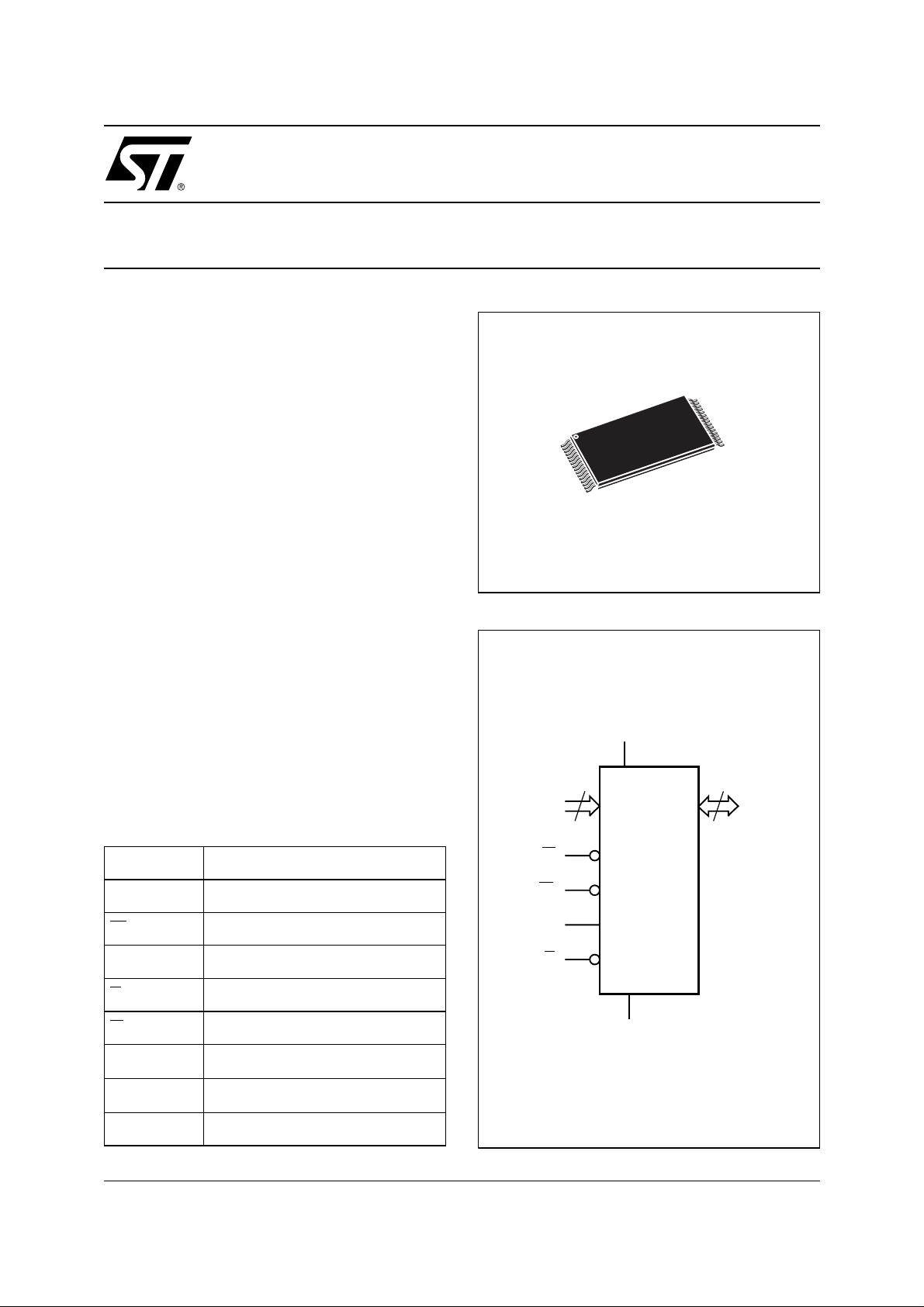
TSOP32 (N)
8 x 20mm
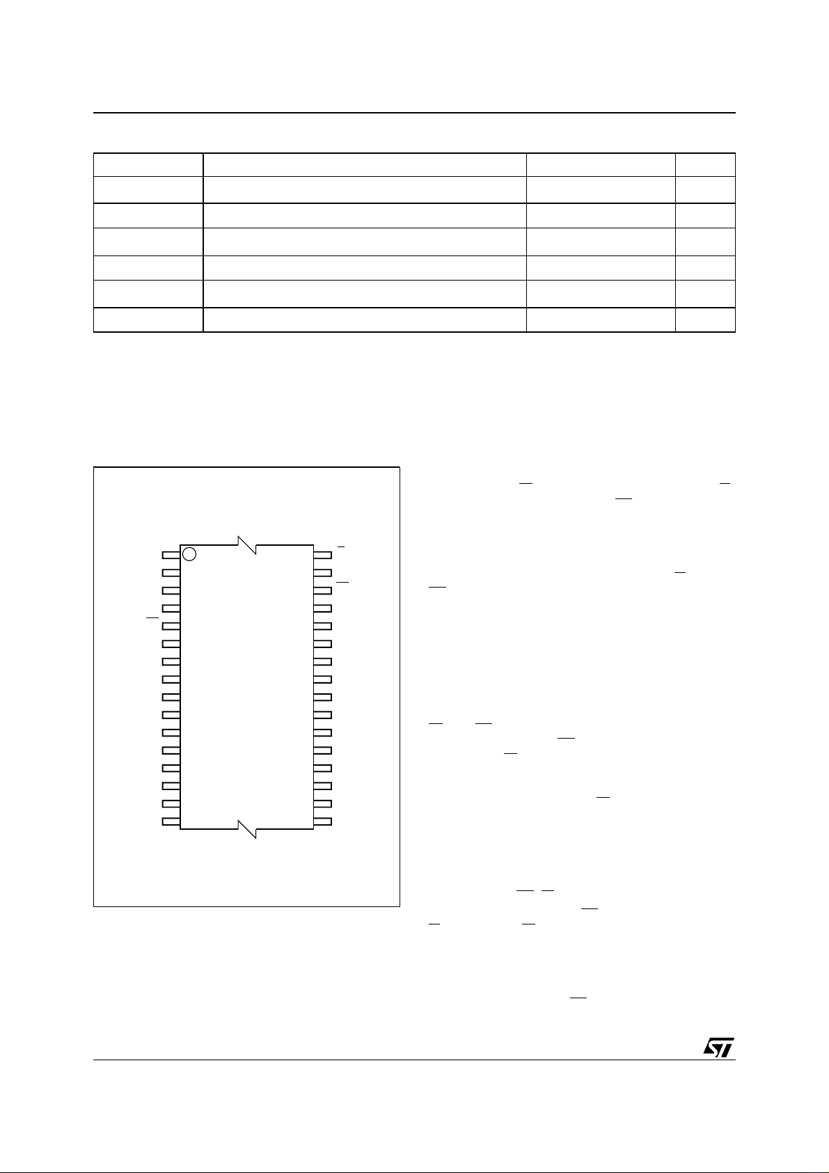
Figure 1. Logic Diagram
DESCRIPTION
The M68Z128 is a 1 Mbit (1,048,576 bit) CMOS
SRAM, organized as 131,072 words by 8 bits. The
device features fully static operat ion requiring no
external clocks or timing strobes, with equal address access and cycle times. It requires a single
5V ±10% supply, and all inputs and outputs are
TTL compatible.
Table 1. Signal Names
A0-A16 Address Inputs
DQ0-DQ7 Data Input/Output
E1
E2 Chip Enable 2
G
W
V
CC
V
SS
Chip Enable 1
Output Enable
Write Enable
Supply Voltage
Ground
A0-A16
W
E1
E2
V
CC
17
M68Z128
G
V
SS
8
DQ0-DQ7
AI00647
NC Not Connected Internally
1/12March 2000
Page 2
M68Z128
Table 2. Absolute Maximum Ratings
Symbol Parameter Value Unit
T
A
T
STG
(2)
V
IO
V
CC
(3)
I
O
P
D
Note: 1. Except for the ratin g " Operating Temperature Range", stresses abo ve those listed in the T able "Abs ol ute Maximum Ratings" may
cause permanent damage to the device. These are stress ratings only and operation of the device at these or any other conditions
above those indi cated in the Operating sections of this s pecification is not impli ed. Exposure to Absolute M aximum Rating conditions for extended per iods may aff ect device reliabilit y. Refer also to the STMicroel ectronics SURE Program an d other relevan t qual ity docum en ts .
2. Up to a m aximum op erating V
3. One out put at a time, not to exceed 1 s econd durat i on.
Ambient Operating Temperature
Storage Temperature –65 to 150 °C
Input or Output Voltage
Supply Voltage –0.3 to 7.0 V
Output Current 20 mA
Power Dissipation 1 W
of 5.5V only.
CC
Figure 2. TSOP Connection s
(1)
READ MODE
0 to 70 °C
–0.3 to V
CC
+ 0.3
V
The M68Z128 is in the Read mode whenever
Write Ena ble (W
Low, and both Chip Enables (E1
) is High with Output Enable (G)
and E2) are asserted. This provides acc ess to dat a fr om eight of
the 1,048,576 locations in the static memory array,
A11 G
1
32
A9
A8
A13
W
E2
A15
V
CC
NC
8
9
M68Z128
25
24
A16
A14
A12
A7
A6
A5
A4 A3
16 17
AI00657
A10
E1
DQ7
DQ6
DQ5
DQ4
DQ3
V
SS
DQ2
DQ1
DQ0
A0
A1
A2
specified by the 17 address inputs. Val id dat a wi ll
be available at the eight output pins within t
AVQV
after the last stable address, providing G is Low,
E1
is Low and E2 is High. If Chip Enable or Output
Enable access times are not met, data access will
be measured from the limiting parameter (t
E2HQV
, or t
t
may be indeterminate at t
) rather than the address. Data out
GLQV
E1LQX
, t
E2HQX
but data lines will always be valid at t
and t
AVQV
E1LQV
GLQX
.
WRITE MODE
The M68Z128 is in the Write mode whenever the
and E1 pins are Low, with E2 High. Either the
W
Chip Enable input s (E1
able input (W
) must be de-asserted during Ad-
and E2) or the Write En-
dress transitions for subsequent write cycles.
Write begins with the concurrence of both Chip
Enables being active with W
low. Therefore, address setup time is r eferenced to Write Enable and
both Chip Enables as t
AVWL
, t
AVE1L
and t
AVE2H
respectively, and is determined by the latter occurring edge.
The Write cycle can be terminated by the earlier
, W, or the falling edge of E2.
= Low, E2 = High and
of its falling edge. Care must
WLQZ
DVWH
or for t
DVE2L
DVE1H
before the
before
be-
This device has an automatic power-down feature,
reducing the power consumption by over 99%
when deselected.
The M68Z128 is available in TSOP32 (8 x 20mm)
package.
rising edge of E1
If the Output is enabled (E1
= Low), then W will return the outputs to high im-
G
pedance within t
be taken to avoid bus contention in this type of operation. Data input must be valid for t
the rising edge of Write E nable, o r for t
fore the rising edge of E1
,
,
2/12
Page 3
Table 3. Operating Modes
Operation E1 E2 W G DQ0-DQ7 Power
Read
Read
Write
Deselect
Deselect X
Note: 1. X = VIH or VIL.
V
IL
V
IL
V
IL
V
IH
V
IH
V
IH
V
IH
V
IH
V
IH
V
IL
XX
V
IL
X
V
IH
V
IL
X
Data Output
Data Input Active
X
X
Hi-Z Active
Hi-Z Standby
Hi-Z Standby
M68Z128
Active
Table 4. AC Measurement Conditions
Figure 3. AC Testing Load Circuit
Input Rise and Fall Times ≤ 15ns
Input Pulse Voltages 0 to 3V
5.0V
Input and Output Timing Ref. Voltages 1.5V
Note: O ut put H i-Z is defin ed as t he poi nt w here da ta is no lo nger
driven.
falling edge of E2, whi chever occurs f irst, and remain v a lid for t
WHDX
, t
E1HDX
or t
E2LDX
.
OPERATIONAL MODE
The M68Z128 has a Chip Enable power down fea-
DEVICE
UNDER
TEST
990Ω
1800Ω
CL = 50pF or 5pF
ture which invokes an automatic standby mode
whenever either Chip Enable is de-asserted (E1
High or E2 = Low). An Output Enable (G
provides a high speed tri-state control, allowing
fast read/write cycles to be achieved with the com-
=
) signal
CL includes JIG capacitance
mon I/O data bu s. Operational mo des are determined by device control inputs W
, E1, and E2 as
summarized in the Operating Modes table.
Table 5. Capacitance
Symbol Parameter Test Condition Min Max Unit
C
IN
(2)
C
OUT
Note: 1. Sampled only, not 100% tested.
2. Outputs desele cted.
(1)
(TA = 25 °C, f = 1 MHz)
Input Capacitance on all pins (except DQ)
Output Capacitance
V
V
OUT
= 0V
IN
= 0V
9pF
9pF
OUT
AI00658B
3/12
Page 4
M68Z128
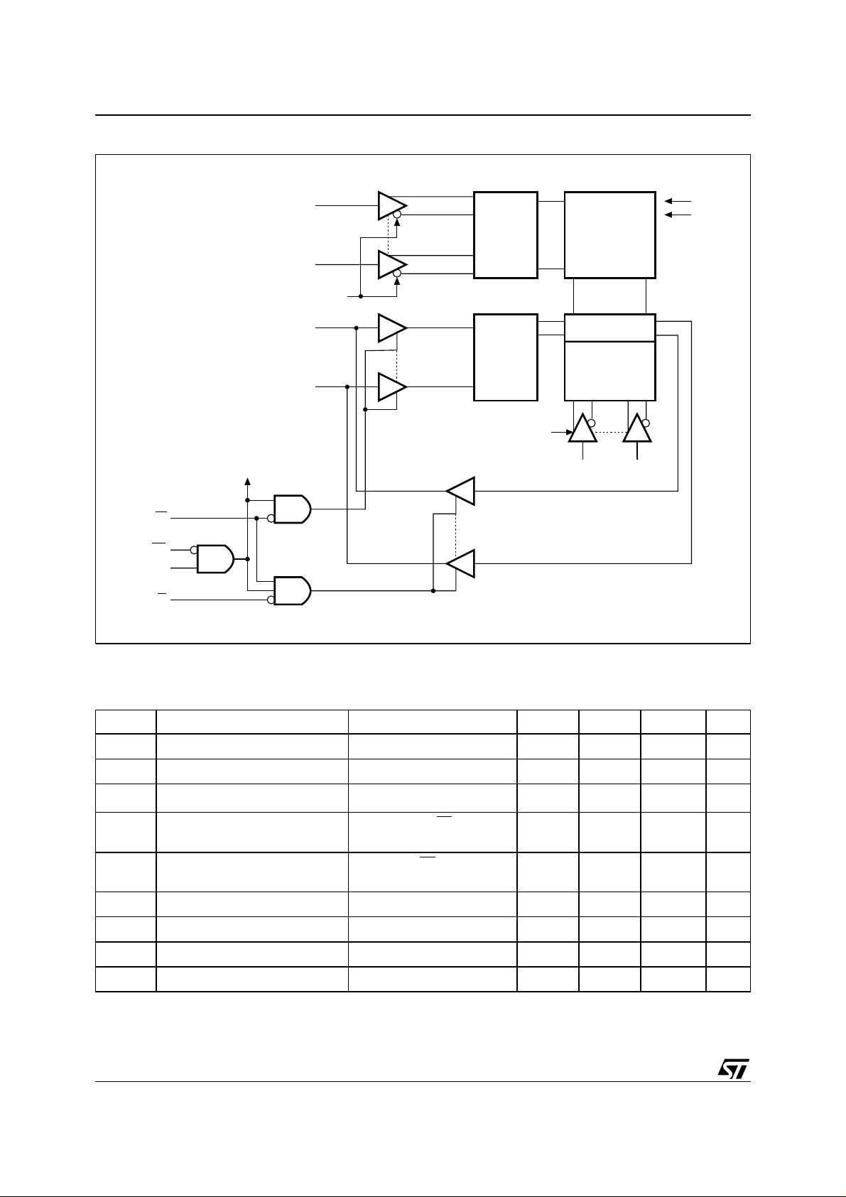
Figure 4. Block Diagram
A
A
CHIP ENABLE.
(9)
ROW
DECODER
MEMORY
ARRAY
V
CC
V
SS
E1
E2
DQ
(8)
DQ
CHIP
ENABLE
W
G
INPUT
DATA
CTRL
CHIP ENABLE.
I/O CIRCUITS
COLUMN
DECODER
(8)
A A
AI00665
Table 6. DC Characteristics
(T
= 0 to 70°C; VCC = 5V ±10%)
A
Symbol Parameter Test Condition Min Typ Max Unit
I
Input Leakage Current
LI
I
I
CC1
I
CC2
I
CC3
V
V
V
V
Note: 1. Average AC current, Ou t puts open, cycling at t
Output Leakage Current
LO
(1)
Supply Current
(2)
Supply Current (Standby) TTL
(3)
Supply Current (Standby) CMOS
Input Low Voltage –0.3 0.8 V
IL
Input High Voltage 2.2
IH
Output Low Voltage
OL
Output High Voltage
OH
2. All other Inputs at V
3. All other Inputs at V
≤ 0.8V or VIH ≥ 2.2V.
IL
≤ 0.3V or VIH ≥ VCC –0.3V.
IL
0V ≤ V
0V
V
V
CC
V
= 5.5V , E1 ≥ V
CC
or E2 ≤ 0.3V, f = 0
minimum.
AVAV
≤ V
IN
CC
≤ V
≤ V
OUT
CC
= 5.5V, (-55)
CC
= 5.5V, E1 = VIH or
E2 = V
I
I
= 2.1mA
OL
= –1mA
OH
IL
, f =0
CC
– 0.3V
±1 µA
±1 µA
30 70 mA
0.1 2 mA
0.4 20 µA
V
+ 0.3
CC
0.4 V
2.4 V
V
4/12
Page 5

M68Z128
Table 7. Read and Standby Modes AC Characteristics
(TA = 0 to 70°C; VCC = 5V ±10%)
Symbol Parameter
t
AVAV
t
AVQV
t
E1LQV
t
E2HQV
t
GLQV
t
E1LQX
t
E2HQX
t
GLQX
t
E1HQZ
t
E2LQZ
t
GHQZ
t
AXQX
t
PU
t
PD
Note: 1. CL = 100pF.
2. C
3. At any given temperature and voltage condition, t
Read Cycle Time 55 ns
(1)
Address Valid to Output Valid 55 ns
(1)
Chip Enable 1 Low to Output Valid 55 ns
(1)
Chip Enable 2 High to Output Valid 55 ns
(1)
Output Enable Low to Output Valid 20 ns
(3)
Chip Enable 1 Low to Output Transition 5 ns
(3)
Chip Enable 2 High to Output Transition 5 ns
(3)
Output Enable Low to Output Transition 0 ns
(2,3)
Chip Enable 1 High to Output Hi-Z 20 ns
(2,3)
Chip Enable 2 Low to Output Hi-Z 20 ns
(2,3)
Output Enable High to Output Hi-Z 20 ns
(1)
Address Transition to Output Transition 5 ns
Chip Enable 1 Low or Chip Enable 2 High to Power Up 0 ns
Chip Enable 1 High or Chip Enable 2 Low to Power Down 55 ns
= 5pF.
L
given devic e.
EIHQZ
+ t
EZHQZ
is less than t
EILQX
and t
M68Z128
Min Max
, t
EZLQX
is less than t
GHQZ
GLQX
Unit-55
for any
Figure 5. Address Controlled, Read Mode AC Waveforms
tAVAV
A0-A16
tAVQV tAXQX
DQ0-DQ7
Note: E1 = Low, E2 = High, G = Low, W = High.
VALID
DATA VALID
AI01078
5/12
Page 6

M68Z128
Figure 6. Chip Enable or Output Enable Controlled, Read Mode AC Waveforms.
tAVAV
A0-A16
tAVQV tAXQX
tE1LQV
E1
tE1LQX
tE2HQV
E2
tE2HQX
G
tGLQX
DQ0-DQ7
Note: Write Enable (W) = High.
Figure 7. Standby Mode AC Waveforms
tGLQV
VALID
tE1HQZ
tE2LQZ
tGHQZ
VALID
AI00805
6/12
E1
E2
I
CC1
I
CC2
tPU
50%
tPD
AI00806B
Page 7

Table 8. Write Mode AC Characteristics
(T
= 0 to 70°C; VCC = 5V ±10%)
A
M68Z128
M68Z128
Symbol Parameter
t
AVAV
t
AVWL
t
AVWH
t
AVE1H
t
AVE2L
t
WLWH
t
WHAX
t
WHDX
t
WHQX
t
WLQZ
t
AVE1L
t
AVE2H
t
E1LE1H
t
E2HE2L
t
E1HAX
t
E2LAX
t
DVWH
t
DVE1H
t
DVE2L
Note: 1. CL = 5pF.
2. At any gi ven temperature and voltage con di tion, t
Write Cycle Time 55 ns
Address Valid to Write Enable Low 0 ns
Address Valid to Write Enable High 45 ns
Address Valid to Chip Enable 1 High 45 ns
Address Valid to Chip Enable 2 Low 45 ns
Write Enable Pulse Width 45 ns
Write Enable High to Address Transition 0 ns
Write Enable High to Input Transition 0 ns
(2)
Write Enable High to Output Transition 5 ns
(1,2)
Write Enable Low to Output Hi-Z 20 ns
Address Valid to Chip Enable 1 Low 0 ns
Address Valid to Chip Enable 2 High 0 ns
Chip Enable 1 Low to Chip Enable 1 High 45 ns
Chip Enable 2 High to Chip Enable 2 Low 45 ns
Chip Enable 1 High to Address Transition 0 ns
Chip Enable 2 Low to Address Transition 0 ns
Input Valid to Write Enable High 25 ns
Input Valid to Chip Enable 1 High 25 ns
Input Valid to Chip Enable 2 Low 25 ns
WHQX
is less than t
for any given device.
WLQZ
Unit-55
Min Max
7/12
Page 8

M68Z128
Figure 8. Write Enable Controlled, Write AC Waveforms
tAVAV
A0-A16
tAVE1L
E1
tAVE2H
E2
tAVWL
W
tWLQZ
DQ0-DQ7
Note: Output E nable (G) = Low.
VALID
tAVWH
tWLWH
Figure 9. Chip Enable Controlled, Write AC Waveforms
tAVAV
tDVWH
(1, 2)
tWHAX
tWHQX
tWHDX
DATA INPUT
AI00807
A0-A16
E1
E2
W
DQ0-DQ7
Note: 1. Output Enable (G) = High.
2. If E1
goes High or E2 goes Low simultaneously with W high, the out put remain s i n a hi gh-impedance state.
VALID
tAVE1H
tAVE1L
tAVE2H tE2HE2L
tAVWL
tE1LE1H
tAVE2L
tDVE1H
tDVE2L
tE1HAX
tE2LAX
tE1HDX
tE2LDX
DATA INPUT
AI00808
8/12
Page 9

M68Z128
Table 9. Low VCC Data Retention Characteristics
(T
= 0 to 70°C)
A
Symbol Parameter Test Condition Min Typ Max Unit
= 3V, E1 ≥ V
V
E1
E1
CC
E2 ≤ 0.3V, f = 0
≥ V
– 0.3V or E2 ≤ 0.3V, f = 0
CC
≥ V
– 0.3V or E2 ≤ 0.3V, f = 0
CC
I
CCDR
V
t
CDR
t
ER
Note: 1. See Figure 10 for measuremen t points. Gu aranteed but not tested. t
Supply Current (Data Retention)
Supply Voltage (Data Retention)
DR
Chip Disable to Power Down
(1)
Operation Recovery Time
Figure 10. Low VCC Data Retention AC Waveforms
5V
VCC 3V
V
> 2.0V
DR
E1 2.2V
tCDR
DATA RETENTION MODE
E1 ≥ V
DR
– 0.3V or
CC
is Read cycl e time.
AVAV
– 0.3V
0.01 2 µA
2V
0ns
t
AVAV
tER
ns
E2 0.8V
E2 ≤ 0.3V
AI00659
9/12
Page 10

M68Z128
Table 10. Ordering Information Scheme
Example: M68Z128 -55 N 1
Device Type
M68Z
Speed
-55 = 55ns
Package
N = TSOP32 (8 x 20mm)
Temperature Range
1 = 0 to 70 °C
For a list of available options (Speed, Pac kage, etc...) or for furthe r information on any aspect of this device, please contact the STMicroelectronics Sales Office nearest to you.
Table 11. Revision History
Date Revision Details
May 1999 First Issue
03/20/00 TSOP32 Package Mechanical Data changed (Table 12)
10/12
Page 11

M68Z128
Table 12. TSOP32 (Type I) - 32 lead Plastic Thin Small Outline, 8 x 20 mm, Package Mechanical Data
Symbol
Typ Min Max Typ Min Max
A 1.200 0.0472
A1 0.050 0.150 0.0020 0.0059
A2 0.950 1.050 0.0374 0.0413
B 0.150 0.270 0.0059 0.0106
C 0.100 0.210 0.0039 0.0083
D 19.800 20.200 0.7795 0.7953
D1 18.300 18.500 0.7205 0.7283
e 0.500 – – 0.0197 – –
E 7.900 8.100 0.3110 0.3189
L 0.500 0.700 0.0197 0.0276
α 0° 5° 0° 5°
CP 0.100 0.0039
N32 32
mm inch
Figure 11. TSOP32 (Type I) - 32 lead Plastic Thin Small Outline, 8 x 20 mm, Package Outline
A2
1 N
e
E
B
N/2
D1
D
DIE
A
CP
C
TSOP-a
Drawing is not to scale.
LA1 α
11/12
Page 12

M68Z128
Information furnished is believed to be accurate and reliable. However, STMicroelec tronics as sumes no responsibility for the consequences
of use of such information nor for any infringement of patents or other rights of third parties which may result from its use. No license is granted
by implic ation or o th erwise u nder any pat ent or pat ent righ ts of STMicroelectron i cs. Specifications m entioned i n this publication are s ubject
to change without notice. This publication supersedes and replaces all information previously supplied. STMicroelectronics products are not
authorized for use as c ritical components in li f e support dev i ces or systems without express writ t en approval of STMicroel ectronics.
The ST log o i s registered trademark of STMic roelectronics
2000 STMicroel e ctronics - All Ri ghts Rese rved
All other names are the property of their respective owners.
Australi a - Brazil - C hi na - Finland - F rance - Germ any - Hong Kong - India - It al y - Japan - Ma la ysia - Malta - Morocco -
Singapor e - Spain - Sweden - Switz erl and - Unit ed K i ngdom - U.S.A.
STMicroelect ro n ics GRO UP OF COMPANI ES
http://www.st.com
12/12
 Loading...