

Page 1
1Mbit (128K x8), 3.0V Asynchronous SRAM
FEATURES SUMMARY
■ SUPPLY VOLTAGE : 2.7 to 3.6V
■ 128K x 8 bits SRAM with OUTPUT ENABLE
■ EQUAL CYCLE and ACCESS TIMES: 70ns
■ LOW STANDBY CURRENT
■ LOW V
■ TRI-STATE COMMON I/O
■ LOW ACTIVE and STAN DBY POWER
DATA RETENTION: 1.5V
CC
M68AW127B
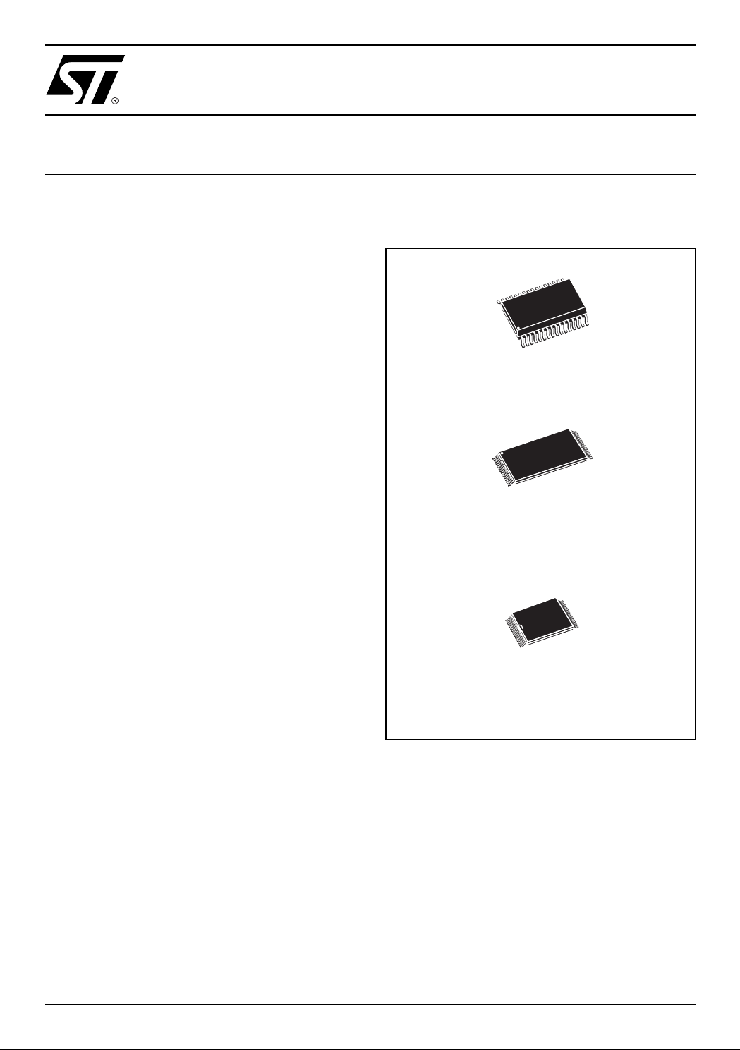
Figure 1. Packages
SO32 (MC)
TSOP32
8 x 20 mm
(N)
TSOP32
8 x 13.4 mm
(NK)
1/20August 2003
Page 2

M68AW127B
TABLE OF CONTENTS
SUMMARY DESCRIPTION. . . . . . . . . . . . . . . . . . . . . . . . . . . . . . . . . . . . . . . . . . . . . . . . . . . . . . . . . . . 3
Figure 2. Logic Diagram . . . . . . . . . . . . . . . . . . . . . . . . . . . . . . . . . . . . . . . . . . . . . . . . . . . . . . . . . . 3
Figure 5. Block Diagram . . . . . . . . . . . . . . . . . . . . . . . . . . . . . . . . . . . . . . . . . . . . . . . . . . . . . . . . . . 5
Figure 3. SO Connections . . . . . . . . . . . . . . . . . . . . . . . . . . . . . . . . . . . . . . . . . . . . . . . . . . . . . . . . . 4
Figure 4. TSOP Connections . . . . . . . . . . . . . . . . . . . . . . . . . . . . . . . . . . . . . . . . . . . . . . . . . . . . . . . 4
Figure 5. Block Diagram . . . . . . . . . . . . . . . . . . . . . . . . . . . . . . . . . . . . . . . . . . . . . . . . . . . . . . . . . . 5
MAXIMUM RATING. . . . . . . . . . . . . . . . . . . . . . . . . . . . . . . . . . . . . . . . . . . . . . . . . . . . . . . . . . . . . . . . . 5
Table 2. Absolute Maximum Ratings. . . . . . . . . . . . . . . . . . . . . . . . . . . . . . . . . . . . . . . . . . . . . . . . . 5
DC AND AC PARAMETERS. . . . . . . . . . . . . . . . . . . . . . . . . . . . . . . . . . . . . . . . . . . . . . . . . . . . . . . . . . 6
Table 3. Operating and AC Measurement Conditions. . . . . . . . . . . . . . . . . . . . . . . . . . . . . . . . . . . . 6
Figure 6. AC Measurement I/O Waveform . . . . . . . . . . . . . . . . . . . . . . . . . . . . . . . . . . . . . . . . . . . .6
Figure 7. AC Measurement Load Circuit . . . . . . . . . . . . . . . . . . . . . . . . . . . . . . . . . . . . . . . . . . . . . .6
Table 4. Capacitance. . . . . . . . . . . . . . . . . . . . . . . . . . . . . . . . . . . . . . . . . . . . . . . . . . . . . . . . . . . . . 7
Table 5. DC Characteristics. . . . . . . . . . . . . . . . . . . . . . . . . . . . . . . . . . . . . . . . . . . . . . . . . . . . . . . . 7
OPERATION . . . . . . . . . . . . . . . . . . . . . . . . . . . . . . . . . . . . . . . . . . . . . . . . . . . . . . . . . . . . . . . . . . . . . . 8
Table 6. Operating Modes. . . . . . . . . . . . . . . . . . . . . . . . . . . . . . . . . . . . . . . . . . . . . . . . . . . . . . . . .8
Read Mode . . . . . . . . . . . . . . . . . . . . . . . . . . . . . . . . . . . . . . . . . . . . . . . . . . . . . . . . . . . . . . . . . . . . 8
Figure 8. Address Controlled, Read Mode AC Waveforms. . . . . . . . . . . . . . . . . . . . . . . . . . . . . . . . 8
Figure 9. Chip Enable or Output Enable Controlled, Read Mode AC Waveforms. . . . . . . . . . . . . . . 9
Table 7. Read and Standby Mode AC Characteristics . . . . . . . . . . . . . . . . . . . . . . . . . . . . . . . . . . 10
Write Mode . . . . . . . . . . . . . . . . . . . . . . . . . . . . . . . . . . . . . . . . . . . . . . . . . . . . . . . . . . . . . . . . . . . 11
Figure 11. Write Enable Controlled, Write AC Waveforms . . . . . . . . . . . . . . . . . . . . . . . . . . . . . . . 11
Figure 12. Chip Enable Controlled, Write AC Waveforms. . . . . . . . . . . . . . . . . . . . . . . . . . . . . . . . 12
Table 8. Write Mode AC Characteristics . . . . . . . . . . . . . . . . . . . . . . . . . . . . . . . . . . . . . . . . . . . . . 13
Figure 13. E1 Controlled, Low V
Figure 14. E2 Controlled, Low V
Data R e t e n tion A C Wavefo r ms . . . . . . . . . . . . . . . . . . . . . . . . 1 4
CC
Data R e t e n tion A C Wavefo r ms . . . . . . . . . . . . . . . . . . . . . . . . 1 4
CC
Table 9. Low VCC Data Retention Characteristics . . . . . . . . . . . . . . . . . . . . . . . . . . . . . . . . . . . . . 14
PACKAGE MECHANICAL . . . . . . . . . . . . . . . . . . . . . . . . . . . . . . . . . . . . . . . . . . . . . . . . . . . . . . . . . . 15
SO32 - 32 lead Plastic Small Outline, Package Outline . . . . . . . . . . . . . . . . . . . . . . . . . . . . . . . . . 15
SO32 - 32 lead Plastic Small Outline, Package Mechanical Data. . . . . . . . . . . . . . . . . . . . . . . . . . 15
TSO P 3 2 - 32 lea d Plastic Small O u tline 8x 2 0 mm, Package Outl i n e. . . . . . . . . . . . . . . . . . . . . . . . 16
TSOP32 - 32 lead Plastic Small Outline 8x20mm, Packag e Mechani ca l Data . . . . . . . . . . . . . . . . 16
TSOP32 - 32 lead Plastic Small Outline 8x13.4mm, Package Outline . . . . . . . . . . . . . . . . . . . . . . 17
TSOP32 - 32 lead Plastic Small Outline 8x13.4mm, Package M ec hanical Data . . . . . . . . . . . . . . 17
PART NUMBERING . . . . . . . . . . . . . . . . . . . . . . . . . . . . . . . . . . . . . . . . . . . . . . . . . . . . . . . . . . . . . . . 18
Table 13. Ordering Information Scheme . . . . . . . . . . . . . . . . . . . . . . . . . . . . . . . . . . . . . . . . . . . . . 18
REVISION HISTORY. . . . . . . . . . . . . . . . . . . . . . . . . . . . . . . . . . . . . . . . . . . . . . . . . . . . . . . . . . . . . . . 19
Table 14. Document Revision History. . . . . . . . . . . . . . . . . . . . . . . . . . . . . . . . . . . . . . . . . . . . . . .19
2/20
Page 3
SUMMARY DESCRIPTION
The M68AW127B is a 1Mbit (1,048,576 bit) CMOS
SRAM, organized as 131,072 words by 8 bits. The
device features fully static operat ion requiring no
external clocks or timing strobes, with equal address access and cycle times. It requires a single
2.7 to 3.6V supply.
This device has an automatic power-down feature,
reducing the power consumption by over 99%
when deselected.
The M68AW127B is available in SO32, TSOP 32
8x20mm and TSOP32 8x13.4mm package s.
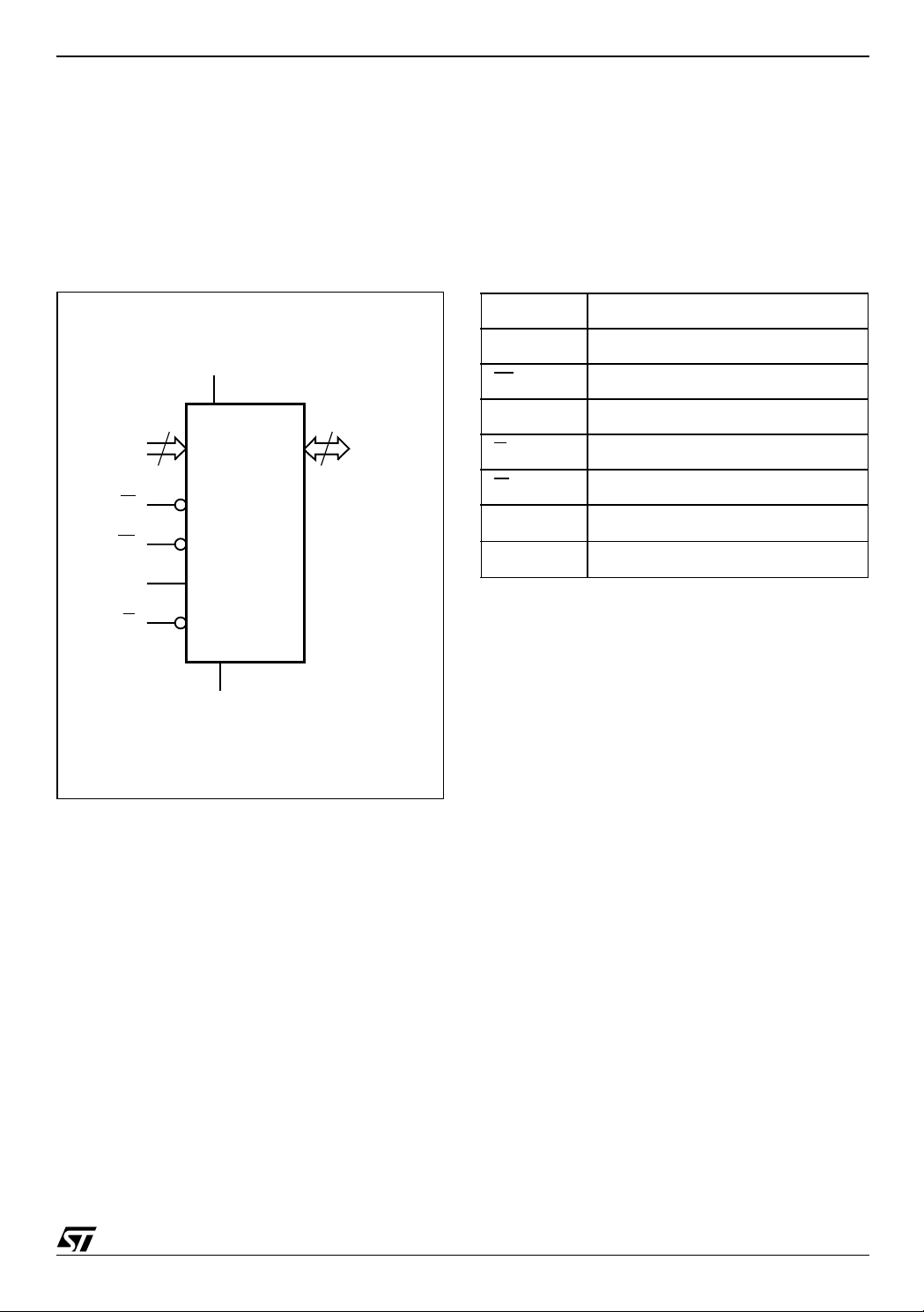
Figure 2. Logic Diagram Table 1. Signal Names
A0-A16 Address Inputs
M68AW127B
A0-A16
W
E1
E2
V
CC
17
M68AW127B
G
V
SS
8
DQ0-DQ7
AI05972b
DQ0-DQ7 Data Input/Output
E1
E2 Chip Enable
G
W
V
CC
V
SS
Chip Enable
Output Enable
Write Enable
Supply Voltage
Ground
3/20
Page 4
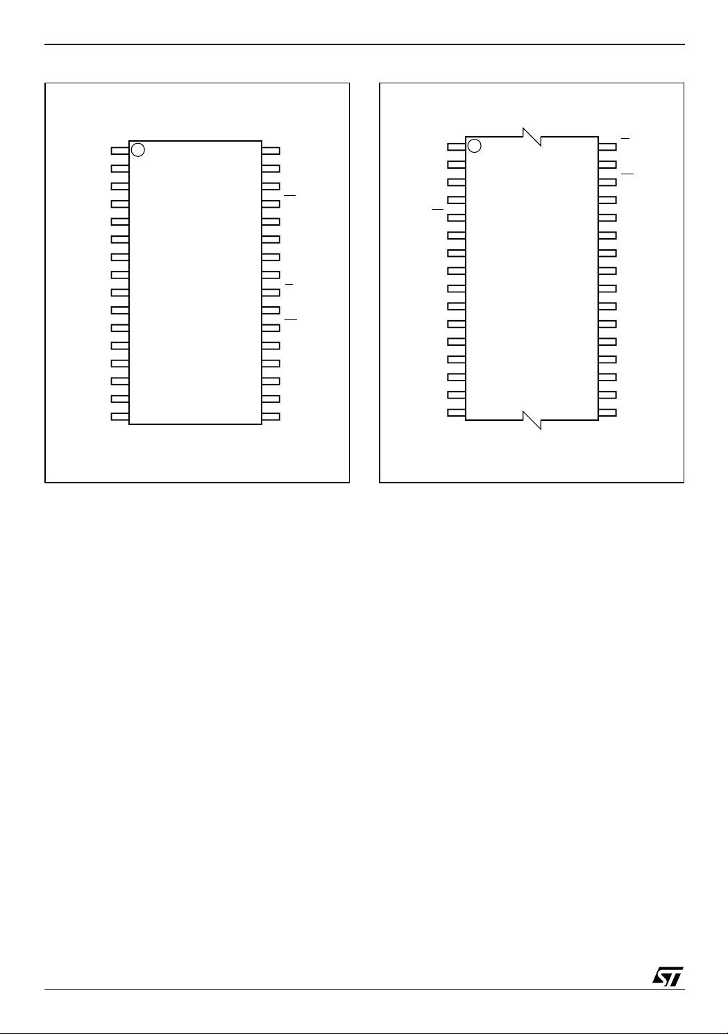
M68AW127B
Figure 3. SO Connections Figure 4. TSOP Connections
NC
A16
A14
A12
A7
A6
A5
A4
A3
A2
A1
A0
DQ0
DQ1
DQ2
V
SS
1
8
M68AW127B
9
32
25
24
16 17
AI05931b
V
CC
A15
E2
W
A13
A8
A9
A11
G
A10
E1
DQ7
DQ6
DQ5
DQ4
DQ3
A11
1
32
A9
A8
A13
W
E2
A15
V
CC
NC
8
M68AW127B
9
25
24
A16
A14
A12
A7
A6
A5
A4 A3
16 17
AI05973c
G
A10
E1
DQ7
DQ6
DQ5
DQ4
DQ3
V
SS
DQ2
DQ1
DQ0
A0
A1
A2
4/20
Page 5
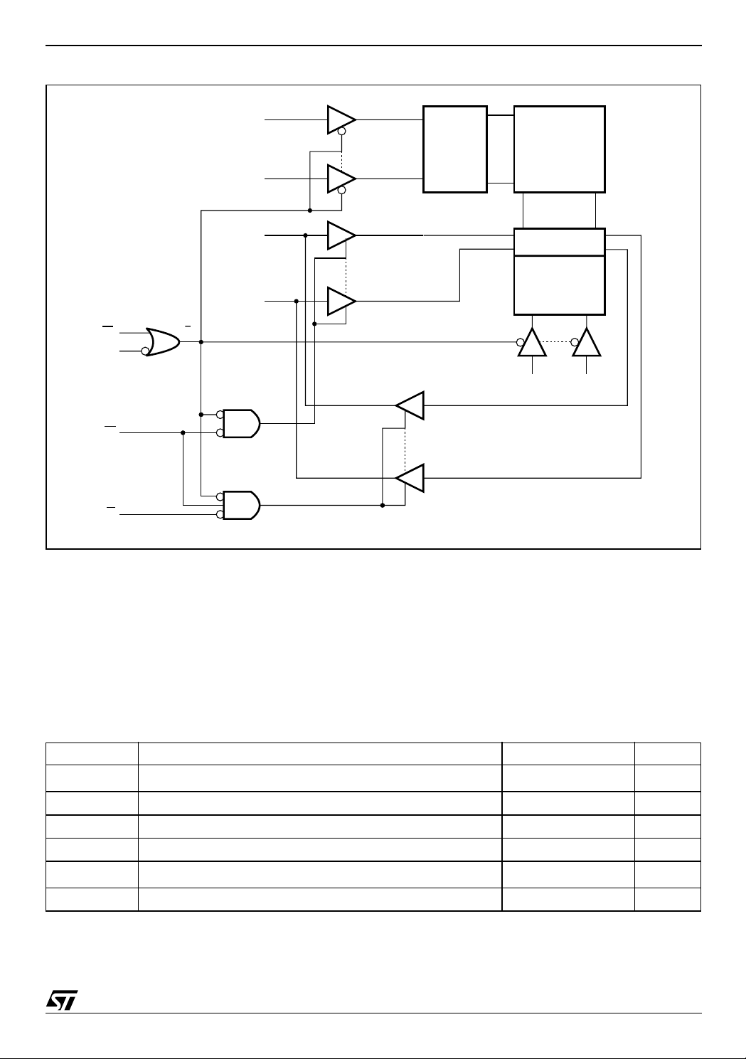
Figure 5. Block Diagram
A16
A7
ROW
DECODER
M68AW127B
MEMORY
ARRAY
DQ7
DQ0
E1
E2
W
G
Ex
MAXIMUM RATIN G
Stressing the device ab ove the rating listed in the
“Absolute Maximum Ratings” table may cause
permanent damage to the device. These are
stress ratings only and operation of the dev ice at
these or any other conditions above those indicated in the Operating sections of this specification is
I/O CIRCUITS
COLUMN
DECODER
A0 A6
AI05471
not implied. Exposure to Absol ute Maxim um Ra ting conditions for extended periods may affect device reliability. Refer also to the
STMicroelectronics SURE Program and other relevant quality documents.
Table 2. Absolute Maximum Ratings
Symbol Parameter Value Unit
(1)
I
O
T
A
T
STG
V
CC
(2)
V
IO
P
D
Note: 1. One output at a time, not to exceed 1 second duration.
2. Up to a maxim um operating V
Output Current 20 mA
Ambient Operating Temperature –55 to 125 °C
Storage Temperature –65 to 150 °C
Supply Voltage –0.3 to 4.6 V
Input or Output Voltage
–0.5 to V
CC
+0.5
Power Dissipation 1 W
of 3.6V only.
CC
V
5/20
Page 6
M68AW127B
DC AND AC PARAMETERS
This section summarizes the operat ing and measurement conditions, as well as the DC and AC
characteristics of the device. The parameters in
the following DC and AC Characteristic tables are
derived from tests performed under the M easure-
Table 3. Operating and AC Measurement Conditions
Parameter M68AW127B
V
Supply Voltage
CC
Ambient Operating Temperature
ment Conditions listed in the rel evant tables. Designers should check that the operating conditions
in their projects match the measurement conditions when using the quoted parameters.
2.7 to 3.6V
Range 1 0 to 70°C
Range 6 –40 to 85°C
Load Capacitance (C
Output Circuit Protection Resis tance (R
Load Resistance (R
)
L
)
1
)
2
100pF
3.0kΩ
3.1kΩ
Input Rise and Fall Times 1ns/V
Input Pulse Voltages
Input and Output Timing Ref. Voltages
Output Transition Timing Ref. Voltages
V
RL
0 to V
CC
V
/2
CC
= 0.3VCC; VRH = 0.7V
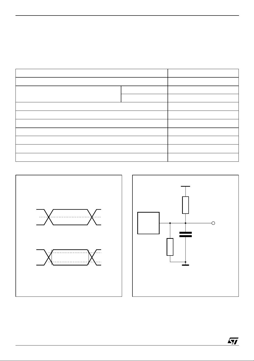
Figure 6. AC Measurement I/O Waveform Figure 7. AC Measurement Load Circuit
V
CC
I/O Timing Reference Voltage
V
CC
0V
Output Transition Timing Reference Voltage
V
CC
0V
VCC/2
0.7V
0.3V
AI04831
DEVICE
UNDER
TEST
R
CC
CC
CL includes JIG capacitance
R
1
OUT
C
L
2
CC
6/20
AI05814
Page 7

M68AW127B
Table 4. Capacitance
Symbol
C
C
OUT
Note: 1. Sampled only, not 100% tested.
2. At T
Input Capacitance on all pins (except DQ)
IN
Output Capacitance
= 25°C, f = 1MHz, VCC = 3.0V.
A
Parameter
(1,2)
Table 5. DC Characteristics
Symbol Parameter Test Condition Min Typ Max Unit
V
I
CC1
I
CC2
(1,2)
Supply Current
Operating Supply Current
Operating Supply Current
(3)
(READ)
Operating Supply Current
(WRITE)
= 3.6V, f = 1/t
CC
I
= 0mA
OUT
V
= 3.6V, f = 1MHz,
CC
I
= 0mA
OUT
= 3.6V, f = 1MHz,
V
CC
I
= 0mA
OUT
AVAV
,
Test
Condition
V
= 0V
IN
V
= 0V
OUT
Min Max Unit
6pF
8pF
70 6.0 15 mA
100 25 35 mA
70 2 mA
1.5 5 mA
100
10 15 mA
I
Input Leakage Current
LI
(4)
I
LO
I
V
V
V
V
Note: 1. Average AC current, cycli ng at t
Output Leakage Current
Standby Supply Current
SB
CMOS
Input High Voltage 2.2
IH
Input Low Voltage
IL
Output High Voltage
OH
Output Low Voltage
OL
= VIL, E2 = VIH, VIN = VIH or VIL.
2. E1
≤ 0.2V or E2 ≥ VCC –0.2V, VIN ≤ 0.2V or VIN ≥ VCC –0.2V.
3. E1
4. Output disab l ed.
AVAV
V
CC
minimum.
0V ≤ V
0V
≤ V
OUT
= 3.6V, E1 ≥ V
E2 ≤ 0.2V, f=0
IOH = –1mA
I
= 2.1mA
OL
IN
≤ V
≤ V
CC
CC
CC
– 0.2V,
–1 1 µA
–1 1 µA
70 2.5 15 µA
100 0.3 10 µA
V
CC
+ 0.3
V
70 –0.3 0.8 V
100 –0.3 0.6 V
70 2.4 V
100 2.2 V
0.4 V
7/20
Page 8

M68AW127B
OPERATION
The M68AW127B has a Chip Enable power down
feature which invokes an automatic standby mode
whenever Chip Enable is de-asserted (E1
or Chip Select is as serted (E2 = Low). An Ou tput
Enable (G
) signal provides a high-s peed, tri-state
Table 6. Operating Modes
Operation E1 E2 W G DQ0-DQ7 Power
= High),
control, allowing fast read/write cycles to be
achieved with the common I /O data bus. Operational modes are determined by device control inputs W
and E1 as summarized in the Operating
Modes table (Table 6).
Read
Read
Write
Deselect
Deselect X
Note: X = VIH or VIL.
V
IL
V
IL
V
IL
V
IH
V
IH
V
IH
V
IH
X X X Hi-Z
V
IL
V
IH
V
IH
V
IL
X X Hi-Z
Read Mode
The M68AW127B is in the Read mode whenever
Write Ena ble (W
Low, Chip Enable (E1
) is High with Output Enable (G)
) is asserted and Chip Select
(E2) is de-asserted. This provid es access to data
from eight of the 1,048,576 loca tions in the static
memory array, specified by the 17 address inputs.
Valid data will be available at the eight output pins
within t
ing G
put Enable access times are not met, data access
will be measured from the limiting parameter
(t
ELQV
may be indeterminate at t
lines will always be valid at t
Figure 8. Address Controlled, Read Mode AC Waveforms
tAVAV
A0-A16
tAVQV tAXQX
VALID
V
IH
V
IL
X Data Input
after the last stable address , provid-
AVQV
Hi-Z
Data Output
Active (I
Active (I
Active (I
Standby (I
Standby (I
CC
CC
CC
SB
SB
)
)
)
)
)
is Low and E1 is Low. If Chip Enable or Out-
or t
) rather than the address. Data out
GLQV
ELQX
AVQV
and t
.
GLQX
, but data
DQ0-DQ7
Note: E1 = Lo w, E 2 = High, G = Low, W = High.
8/20
DATA VALID
AI05474
Page 9

Figure 9. Chip Enable or Output Enable Controlled, Read Mode AC Waveforms.
tAVAV
M68AW127B
A0-A16
tAVQV tAXQX
tELQV
E1
E2
tELQX
tGLQV
G
tGLQX
DQ0-DQ7
Note: Write Enable (W) = High.
VALID
VALID
Figure 10. Chip Enable Controlled, Standby Mode AC Waveforms
tEHQZ
tGHQZ
AI05476
E1
E2
I
I
CC
SB
tPU
50%
tPD
AI05477
9/20
Page 10

M68AW127B
Table 7. Read and Standby Mode AC Characteristics
Symbol Parameter
t
AVAV
t
AVQV
t
AXQX
t
EHQZ
t
ELQV
t
ELQX
t
GHQZ
t
GLQV
t
GLQX
(4)
t
PD
(4)
t
PU
Note: 1. Test con di tions as s u m e t ransit i on timing reference lev el = 0.3VCC or 0.7VCC.
2. At any given temperature and voltage con di tion, t
3. These parameters are defined as the time at which the outputs achieve the open circuit conditions and are not referenced to output
4. T ested initial l y and after any design or process changes t hat may affect these parameters.
Read Cycle Time Min 70 100 ns
Address Valid to Output Valid Max 70 100 ns
(1)
Data hold from address change Min 5 15 ns
(2,3)
Chip Enable High to Output Hi-Z Max 25 30 ns
Chip Enable Low to Output Valid Max 70 100 ns
(1)
Chip Enable Low to Output Transition Min 5 10 ns
(2,3)
Output Enable High to Output Hi-Z Max 25 30 ns
Output Enable Low to Output Valid Max 35 50 ns
(2)
Output Enable Low to Output Transition Min 5 5 ns
Chip Enable or UB/LB High to Power Down Max 0 0 ns
Chip Enable or UB/LB Low to Power Up Min 70 100 ns
voltage lev el s.
is less than t
GHQZ
GLQX
and t
is less than t
EHQZ
M68AW127B
70 100
for any given device.
ELQX
Unit
10/20
Page 11

Write Mode
The M68AW127B is in the Write mode whenever
and E1 pins are Low and the E2 pin is High.
the W
Either the Chip Enable input (E1
able input (W
) must be de-asserted during Ad-
) or the Write En-
dress transitions for subsequent write cycles.
Write begins with the concurrence of E1
tive w ith W
low. Therefore, address setup time is
being ac-
referenced to Write Enable and Chip Enable as
t
AVWL
and t
, respectively, an d is determined
AVEH
by the latter occurring edge.
The Write cycle can be terminated by the earlier
rising edge of E1
If the Output is enabled (E1
G
= Low), then W will return the outputs to high impedance within t
be taken to avoid bus contention in this type of operation. Data input must be valid for t
the rising edge of Write Enable, or for t
the rising edge of E1
remain valid for t
Figure 11. Write Enable Controlled, Write AC Waveforms
tAVAV
M68AW127B
, or W.
= Low, E2 = High and
of its falling edge. Care must
WLQZ
DVWH
, whichever occurs first, and
or t
WHDX
EHDX
DVEH
.
before
before
A0-A16
E1
E2
W
DQ0-DQ7
tAVEL
tAVWL
tWLQZ
VALID
tAVWH
tELWH
tWLWH
tWHAX
tWHQX
tWHDX
DATA INPUT
tDVWH
AI05478
11/20
Page 12

M68AW127B
Figure 12. Chip Enable Controlled, Write AC Waveforms
tAVAV
A0-A16
E1
E2
W
DQ0-DQ7
tAVWL
tAVEL
VALID
tAVEH
tWLEH
tELEH
tEHAX
tEHDX
DATA INPUT
tDVEH
AI05479
12/20
Page 13

M68AW127B
Table 8. Write Mode AC Characteristics
Symbol Parameter
t
AVAV
t
AVEH
t
AVEL
t
AVWH
t
AVWL
t
DVEH
t
DVWH
t
EHAX
t
EHDX
t
ELEH
t
ELWH
t
WHAX
t
WHDX
t
WHQX
t
WLEH
t
WLQZ
t
WLWH
Note: 1. At any gi ven temperature and voltage condit i on, t
2. These parameters are defined as the time at which the outputs achieve the open circuit conditions and are not referenced to output
Write Cycle Time Min 70 100 ns
Address Valid to Chip Enable High Min 60 80 ns
Address valid to Chip Enable Low Min 0 0 ns
Address Valid to Write Enable High Min 60 80 ns
Address Valid to Write Enable Low Min 0 0 ns
Input Valid to Chip Enable High Min 30 40 ns
Input Valid to Write Enable High Min 30 40 ns
Chip Enable High to Address Transition Min 0 0 ns
Chip enable High to Input Transition Min 0 0 ns
Chip Enable Low to Chip Enable High Min 60 80 ns
Chip Enable Low to Write Enable High Min 60 80 ns
Write Enable High to Address Transition Min 0 0 ns
Write Enable High to Input Transition Min 0 0 ns
(1)
Write Enable High to Output Transition Min 5 5 ns
Write Enable Low to Chip Enable High Min 60 70 ns
(1,2)
Write Enable Low to Output Hi-Z Max 20 30 ns
Write Enable Low to Write Enable High Min 60 70 ns
voltage lev el s.
is less than t
WLQZ
for any given device.
WHQX
M68AW127B
70 100
Unit
13/20
Page 14

M68AW127B
Figure 13. E1 Controlled, Low VCC Data Retention AC Waveforms
3.6V
VCC 2.7V
E1
> 1.5V
(1)
V
DR
Note: 1. For 100ns spee d cl ass VDR ≥ 2.0V.
tCDR
DATA RETENTION MODE
E1 ≥ V
DR
– 0.2V
Figure 14. E2 Controlled, Low VCC Data Retention AC Waveforms
3.6V
VCC 2.7V
> 1.5V
(1)
V
DR
E2
tCDR
DATA RETENTION MODE
E2 ≤ 0.2V
tR
AI05980
tR
AI05957B
Note: 1. For 100ns spee d cl ass VDR ≥ 2.0V.
Table 9. Low VCC Data Retention Characteristics
Symbol Param eter Test Condition Min Typ Max Unit
= 1.5V, E1 ≥ V
CCDR
t
CDR
t
R
V
DR
Note: 1. All other Inputs at VIH ≥ V
(Data Retention)
Chip Deselected to Data
(1,2)
Retention Time
(2)
Operation Recovery Time
Supply Voltage
(1)
(Data Retention)
–0.2V or VIL ≤ 0.2V.
2. T ested initial l y and after any design or process that may af fect these pa ram eters.
3. No input may exceed V
CC
CC
+0.2V.
Supply Current
(1)
I
V
CC
E2 ≤ 0.2V, f = 0
≥ V
E1
CC
E2 ≤ 0.2V, f = 0
–0.2V or
CC
–0.2V or
70 4.5 µA
100 5 µA
0ns
70
t
AVAV
100 5 ms
70 1.5 V
100 2.0 V
t
is Read cycl e time.
AVAV
ns
14/20
Page 15

PACKAGE MECHANICAL
Figure 15. SO32 - 32 lead Plastic Small Outline, Package Outline
D
M68AW127B
16
17 32
B
e
1
E
E1
A2
A1
A
CP
L1
SO-C
Note: Drawing is not to scale.
Table 10. SO32 - 32 lead Plastic Small Outline, Package Mechanical Data
Symbol
Typ Min Max Typ Min Max
A 2.997 0.118
millimeters inches
C
L
A1 0.102 0.004
A2 2.565 2.819 0.101 0.111
b 0.356 0.508 0.014 0.020
c 0.152 0.305 0.006 0.012
D 20.142 20.7 52 0.793 0.817
E 11.176 11.430 0.440 0.450
E1 13.868 14.376 0.546 0.566
e 1.270 – – 0.050 – –
L 0.584 0.991 0.023 0.039
L1 1.194 1.600 0. 047 0.063
CP 0.10 0.004
15/20
Page 16

M68AW127B
Figure 16. TSOP32 - 32 lead Plastic Small Outline 8x20mm, Package Outline
A2
1 N
E
N/2
e
B
D1
D
DIE
A
CP
C
TSOP-a
Note: Drawing is not to scale.
LA1 α
Table 11. TSOP32 - 32 lead Plastic Small Outline 8x20mm, Package M echa nical Data
Symbol
Typ Min Max Typ Min Max
A 1.200 0.0472
A1 0.050 0.150 0.0020 0.0059
A2 0.950 1.050 0.0374 0.0413
B 0.170 0.250 0.0067 0 .0098
C 0.100 0.210 0.0039 0.0083
millimeters inches
CP 0.100 0.0039
D 19.800 20.2 00 0.7795 0.7953
D1 18.300 18.5 00 0.7205 0.7283
E 7.900 8.100 0.3110 0.3189
e 0.500 – – 0.01 97 – –
L 0.500 0.700 0.0197 0.0276
α 0° 5° 0 ° 5°
N32 32
16/20
Page 17

Figure 17. TSOP32 - 32 lead Plastic Small Outline 8x13.4mm, Package Outline
A2
1 N
e
E
B
N/2
M68AW127B
D1
D
DIE
A
CP
C
TSOP-a
Note: Drawing is not to scale.
LA1 α
Table 12. TSOP32 - 32 lead Plastic Small Outline 8x13.4mm, Packa ge Mechan ic al Data
Symbol
Typ Min Max Typ Min Max
A 1.20 0.0472
A1 0.05 0.15 0.0 020 0.0059
A2 0.91 1.05 0.0 358 0.0413
B 0.22 0.0087
C 0.10 0.21 0.0039 0.0083
millimeters inches
D 13.40 – – 0.5276 – –
D1 11.80 – – 0.46 46 – –
E 8.00 – – 0.3150 – –
e 0.50 – – 0.0197 – –
L 0.40 0.60 0.0157 0.0236
α 05 05
N32 32
CP 0.10 0.0039
17/20
Page 18

M68AW127B
PART NUMBERING
Table 13. Ordering Information Scheme
Example: M68AW127 B L 70 N 6 T
Device Type
M68
Mode
A = Asynchronous
Operating Voltage
W = 2.7 to 3.6V
Array Organization
127 = 1Mbit (128K x8)
Option 1
B = 2 Chip Enable
Option 2
L = L-Die
M = M-Die
Speed Class
70 = 70ns
10 = 100ns
Package
MC = SO32
N = TSOP32 (8 x 20 mm)
NK = TSOP32 (8 x 13.4 mm)
Operative Temperature
1 = 0 to 70°C
6 = –40 to 85 °C
Shipping
T = Tape & Reel Packing
For a list of available options (e.g., Speed, Package) or for further information on any aspect of this device,
please contact the STMicroelectronics Sales Office nearest to you.
18/20
Page 19

REVISION HIST ORY
Table 14. Document Revision History
Date Version Revision Details
January 2002 1.0 First Issue
DC Characteristics table clarified (Table 5)
E1
09-May-2002 2.0
01-Jul-2002 3.0
11-Sep-2002 4.0 Commercial code clarified
02-Oct-2002 4.1 Title and header layout modified.
09-Oct-2002 4.2 Commercial code modified.
16-Apr-2003 4.3
21-Aug-2003 4.4 TSOP Package connections modified (Figure 5)
Controlled, Low VCC Data Retention AC Waveforms clarified (Figure 13)
Low V
Ordering Information Scheme clarified (Table 13)
70ns speed class added
SO32 and TSOP32 8x13.4mm package options added
Label corrected on “E2 Controlled, Low V
Data Retention Characteristics table clarified (Table 9)
CC
M68AW127B
Data Retention AC Waveforms” figure
CC
19/20
Page 20

M68AW127B
Information furnished is believed to be ac curate and reliable. Howev er, STMicroelec tronics assumes no respon si bility for the consequence s
of use of such information nor for any infringement of patents or other rights of third parties which may result from its use. No license is granted
by implic ation or oth erwise under any patent or patent rights of STMicroe l ectronics. Specificati ons mentioned in this publication are subject
to change without notice. This publication supersedes and replaces all information previously supplied. STMicroelectronics products are not
authorized for use as critical comp onents in life su pport device s or systems without express written ap proval of STMi croelectronics.
The ST log o i s registered trademark of STM i croelectronics
All other names are the p roperty of the i r respectiv e owners.
© 2003 STMicroelectronics - All Rights Reserved
Australi a - Brazil - Canada - China - F i nl and - France - Germany - Hong Kong - India - Israel - Italy - Japan - Malay sia - Malta -
Morocc o - Singapore - Spain - Swed en - S wi tzerland - United Kingdom - United States
STMicroelectron ics GROUP OF COMPANIES
www.st.com
20/20
 Loading...