

Page 1
1 Mbit (64K x16) 3.0V Asynchro nous SRAM
FEATURES SUMMARY
■ SUPPLY VOLTAGE : 2.7 to 3.6V
■ 64K x 16 bits SRAM with OUTPUT ENABLE
■ EQUAL CYCLE and ACCESS TIME: 55ns and
70ns
■ LOW STANDBY CURRENT
■ LOW V
■ TRI-STATE COMMON I/O
■ AUTOMATIC POWER DOWN
DATA RETENTION: 2.0V
CC
M68AW0 64F
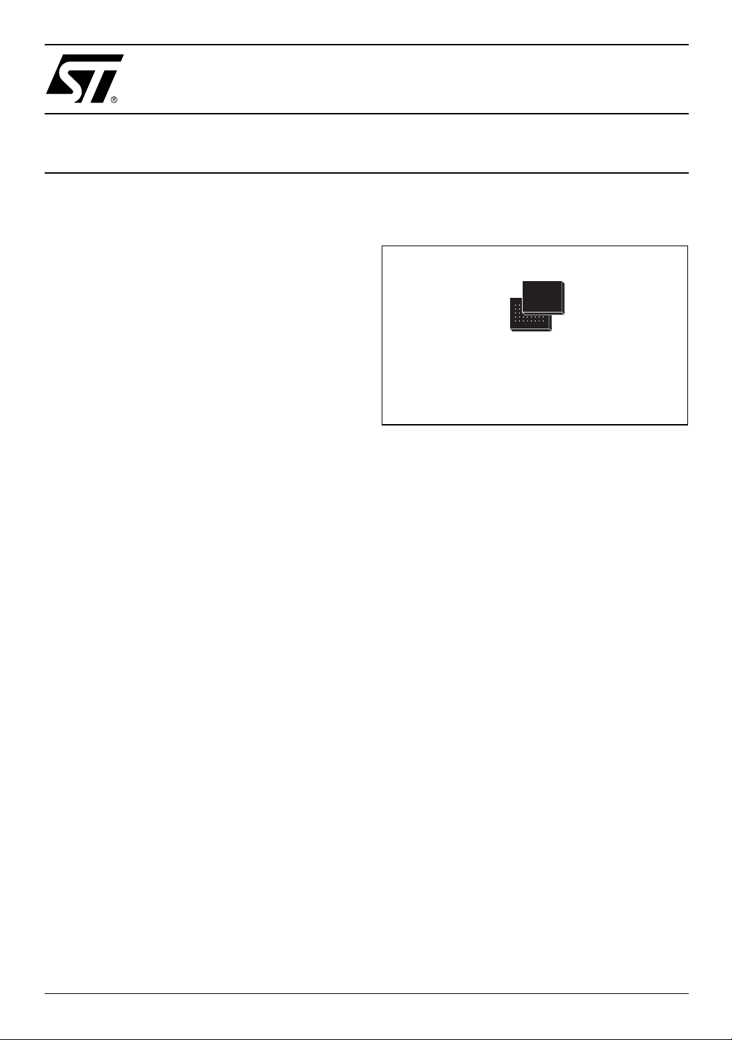
Figure 1. Packages
BGA
TFBGA48 (ZB)
6 x 8 solder balls
1/18April 2003
Page 2

M68AW064F
TABLE OF CONTENTS
SUMMARY DESCRIPTION. . . . . . . . . . . . . . . . . . . . . . . . . . . . . . . . . . . . . . . . . . . . . . . . . . . . . . . . . . . 3
Figure 2. Logic Diagram . . . . . . . . . . . . . . . . . . . . . . . . . . . . . . . . . . . . . . . . . . . . . . . . . . . . . . . . . . 3
Table 1. Signal Names . . . . . . . . . . . . . . . . . . . . . . . . . . . . . . . . . . . . . . . . . . . . . . . . . . . . . . . . . . . 3
Figure 3. TFBGA Connections (Top view through package). . . . . . . . . . . . . . . . . . . . . . . . . . . . . . . 4
Figure 4. Block Diagram . . . . . . . . . . . . . . . . . . . . . . . . . . . . . . . . . . . . . . . . . . . . . . . . . . . . . . . . . . 5
MAXIMUM RATING. . . . . . . . . . . . . . . . . . . . . . . . . . . . . . . . . . . . . . . . . . . . . . . . . . . . . . . . . . . . . . . . . 5
Table 2. Absolute Maximum Ratings. . . . . . . . . . . . . . . . . . . . . . . . . . . . . . . . . . . . . . . . . . . . . . . . . 5
DC AND AC PARAMETERS. . . . . . . . . . . . . . . . . . . . . . . . . . . . . . . . . . . . . . . . . . . . . . . . . . . . . . . . . . 6
Table 3. Operating and AC Measurement Conditions. . . . . . . . . . . . . . . . . . . . . . . . . . . . . . . . . . . . 6
Figure 5. AC Measurement I/O Waveform . . . . . . . . . . . . . . . . . . . . . . . . . . . . . . . . . . . . . . . . . . . . 6
Figure 6. AC Measurement Load Circuit . . . . . . . . . . . . . . . . . . . . . . . . . . . . . . . . . . . . . . . . . . . . . .6
Table 4. Capacitance. . . . . . . . . . . . . . . . . . . . . . . . . . . . . . . . . . . . . . . . . . . . . . . . . . . . . . . . . . . . . 7
Table 5. DC Characteristics. . . . . . . . . . . . . . . . . . . . . . . . . . . . . . . . . . . . . . . . . . . . . . . . . . . . . . . . 7
OPERATION . . . . . . . . . . . . . . . . . . . . . . . . . . . . . . . . . . . . . . . . . . . . . . . . . . . . . . . . . . . . . . . . . . . . . . 8
Table 6. Operating Modes. . . . . . . . . . . . . . . . . . . . . . . . . . . . . . . . . . . . . . . . . . . . . . . . . . . . . . . . . 8
Read Mode . . . . . . . . . . . . . . . . . . . . . . . . . . . . . . . . . . . . . . . . . . . . . . . . . . . . . . . . . . . . . . . . . . . . 8
Figure 7. Address Controlled, Read Mode AC Waveforms. . . . . . . . . . . . . . . . . . . . . . . . . . . . . . . . 8
Figure 8. Chip Enable or Output Enable Controlled, Read Mode AC Waveforms. . . . . . . . . . . . . . . 9
Figure 9. Chip Enable or UB/LB Controlled, Standby Mode AC Waveforms . . . . . . . . . . . . . . . . . . 9
Table 7. Read and Standby Mode AC Characteristics . . . . . . . . . . . . . . . . . . . . . . . . . . . . . . . . . . 10
Write Mode . . . . . . . . . . . . . . . . . . . . . . . . . . . . . . . . . . . . . . . . . . . . . . . . . . . . . . . . . . . . . . . . . . . 11
Figure 10. Write Enable Controlled, Write AC Waveforms . . . . . . . . . . . . . . . . . . . . . . . . . . . . . . . 11
Figure 11. Chip Enable Controlled, Write AC Waveforms. . . . . . . . . . . . . . . . . . . . . . . . . . . . . . . . 12
Table 8. Write Mode AC Characteristics . . . . . . . . . . . . . . . . . . . . . . . . . . . . . . . . . . . . . . . . . . . . . 13
Figure 12. Low V
Table 9. Low V
Data Retention AC Waveforms. . . . . . . . . . . . . . . . . . . . . . . . . . . . . . . . . . . . 14
CC
Data Retention Characteristics. . . . . . . . . . . . . . . . . . . . . . . . . . . . . . . . . . . . . . 14
CC
PACKAGE MECHANICAL . . . . . . . . . . . . . . . . . . . . . . . . . . . . . . . . . . . . . . . . . . . . . . . . . . . . . . . . . . 15
TFBGA48 - 6 x 8 ball array, 0.75 mm pitch, Bottom View Package Outline . . . . . . . . . . . . . . . . . . 15
TFBGA48 - 6 x 8 ball array, 0.75 mm pitch, Package Mechanical Data . . . . . . . . . . . . . . . . . . . . . 15
PART NUMBERING . . . . . . . . . . . . . . . . . . . . . . . . . . . . . . . . . . . . . . . . . . . . . . . . . . . . . . . . . . . . . . . 16
Table 11. Ordering Information Scheme . . . . . . . . . . . . . . . . . . . . . . . . . . . . . . . . . . . . . . . . . . . . . 16
REVISION HISTORY. . . . . . . . . . . . . . . . . . . . . . . . . . . . . . . . . . . . . . . . . . . . . . . . . . . . . . . . . . . . . . . 17
Table 12. Document Revision History. . . . . . . . . . . . . . . . . . . . . . . . . . . . . . . . . . . . . . . . . . . . . . .17
2/18
Page 3
SUMMARY DESCRIPTION
The M68AW064F is a 1 Mbit (1,048,576 bit)
CMOS SRAM, organized as 65,536 words by 16
bits. The device features fully static opera tion requiring no external clocks or timing strobes, with
equal address access and cycle times. It requires
tomatic power-down feature, redu cing the power
consumption by over 99% when deselected.
The M68AW064F is available in TFBGA48 (0.75
mm pitch) package.
a single 2.7 to 3.6V supply. This device has an au-
Figure 2. Logic Diagram Table 1. Signal Names
A0-A15 Address Inputs
V
CC
DQ0-DQ15 Data Input/Output
M68AW064F
A0-A15
W
UB
LB
16
16
DQ0-DQ15
E
M68AW064F
G
V
SS
AI04872b
E
G
W
UB
LB
V
CC
V
SS
NC Not Connected Internally
Chip Enable
Output Enable
Write Enable
Upper Byte Enable Input
Lower Byte Enable Input
Supply Voltage
Ground
3/18
Page 4
M68AW064F
Figure 3. TFBGA Connections (Top view through package)
654321
A
B
C
D
E
F
G
H
DQ8
DQ9
V
SS
V
CC
DQ14
DQ15
UB
DQ10
DQ11
DQ12
DQ13
NC
A0GLB
NC
NC V
A14
A9
A1
A4 E
A6A5
A7
NC
A15
A13
A10
A2 NC
DQ3
DQ4
DQ5
DQ0A3
DQ2DQ1
V
CC
SS
DQ6
DQ7WA12
NCA11A8NC
4/18
AI04874
Page 5
Figure 4. Block Diagram
A15
A7
ROW
DECODER
MEMORY
ARRAY
M68AW064F
V
CC
V
SS
DQ15
UB
DQ0
LBLB
W
UB
LB
E
G
MAXIMUM RATI NG
Stressing the device ab ove the rating listed in t he
Absolute Maximum Ratings" table may cause permanent damage to the device. These are stress
ratings only and operation of the device at these or
any other conditions ab ove those i ndicated in t he
Operating sections of this specificat ion is not im-
(8)
(8)
(8)
UB
(8)
LB
I/O CIRCUITS
COLUMN
DECODER
A0 A6
AI04875
plied. Exposure to Absolute Maximum Rating conditions for extended periods may affect device
reliability. Refer also to the STMicroelectronics
SURE Program and ot her relevant quality documents.
Table 2. Absolute Maximum Ratings
Symbol Parameter Value Unit
(1)
I
O
T
A
T
STG
V
CC
(2)
V
IO
P
D
Note: 1. One out put at a time, not to exceed 1 second durat i on.
2. Up to a maxim um operating V
Output Current 20 mA
Ambient Operating Temperature –55 to 125 °C
Storage Temperature –65 to 150 °C
Supply Voltage –0.5 to 4.6 V
Input or Output Voltage
–0.5 to V
CC
+0.5
Power Dissipation 1 W
of 3.6V only.
CC
V
5/18
Page 6
M68AW064F
DC AND AC PARAMETERS
This section summarizes the operat ing and measurement conditions, as well as the DC and AC
characteristics of the device. The parameters in
the following DC and AC Characteristic tables are
derived from tests performed under the M easure-
Table 3. Operating and AC Measurement Conditions
Parameter M68AW064F
Supply Voltage
V
CC
Ambient Operating Temperature –40 to 85°C
Load Capacitance (C
Output Circuit Protection Resis tance (R
Load Resistance (R
Input Rise and Fall Times
Input Pulse Voltages
Input and Output Timing Ref. Voltages
Input and Output Transition Timing Ref. Voltages
)
L
)
1
)
2
ment Conditions listed in the rel evant tables. Designers should check that the operating conditions
in their projects match the measurement conditions when using the quoted parameters.
2.7 to 3.6V
30 or 5pF
1.10k
1.55k
4ns
≤
0 to V
V
CC
V
= 0.3VCC; VOH = 0.7V
OL
Ω
Ω
CC
/2
CC
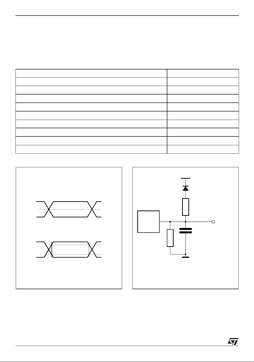
Figure 5. AC Measurement I/O Waveform Figure 6. AC Measurement Load Circuit
V
CC
I/O Timing Reference Voltage
V
CC
0V
I/O Transition Timing Reference Voltage
V
CC
0V
VCC/2
0.7V
0.3V
AI04831
CC
CC
DEVICE
UNDER
TEST
R
2
CL includes JIG capacitance
1N914
R
1
OUT
C
L
AI03853
6/18
Page 7

Table 4. Capacitance
Symbol
C
C
OUT
Note: 1. Sampled only, not 100% tested.
2. At T
3. Outputs desel ected.
Input Capacitance on all pins (except DQ)
IN
(3)
Output Capacitance
= 25°C, f = 1 MHz, VCC = 3.0V.
A
Table 5. DC Characteristics
Parameter
(1,2)
Test
Condition
V
= 0V
IN
V
= 0V
OUT
M68AW064F
M68AW064F
Min Max Unit
6pF
8pF
Symbol Parameter Test Condition
= 3.6V, f = 1/t
V
AVAV
CC
I
OUT
= 3.6V, f = 1MHz,
V
CC
I
OUT
V
CC
E
≥ V
–0.15V, f = 0
CC
0V ≤ V
V
0V
≤
OUT
V
CC
V
CC
V
CC
I
= –1.0mA
OH
V
CC
I
= 2.1mA
OL
minimum.
= 0mA
= 0mA
= 3.6V,
≤ V
IN
≤ V
= 2.7V
= 2.7V
= 2.7V,
= 2.7V,
CC1
I
CC2
I
SB
I
V
V
V
V
Note: 1. Aver age AC curre nt, cycling at t
Current
Operating Supply
Current
Standby Supply Current
(2)
CMOS
I
Input Leakage Curren t
LI
Output Leakage Current
LO
Input High Voltage
IH
Input Low Voltage
IL
Output High Voltage
OH
Output Low Voltage
OL
2. All other Inputs at V
3. Output disabled.
≤ 0.15V or VIH ≥ VCC –0.15V.
IL
Operating Supply
(1)
I
CC
CC
Min Typ Max Min Typ Max
,
AVAV
720 15mA
12 12mA
0.5 15 0.5 15 µA
–1 1 –1 1 µA
(3)
–1 1 –1 1 µA
V
2.0
CC
+ 0.3
2.0
–0.3 0.4 –0.3 0.4 V
2.2 2.2 V
0.4 0.4 V
Unit55 70
V
CC
+ 0.3
V
7/18
Page 8

M68AW064F
OPERATION
The M68AW064F has a Chip Enable power down
feature which invokes an automatic standby mode
whenever either Chip Enable is de-asserted
= High) or LB and UB are de-asserted (LB and
(E
UB
= High). An Output Enable (G) signal provides
Table 6. Operating Modes
Operation E W G LB UB DQ0-DQ7 DQ8-DQ15 Power
Deselected/Power-down
Deselected/Power-down X X X
Lower Byte Read
Lower Byte Write
Output Disabled
Output Disabled
Upper Byte Read
Upper Byte Write
Word Read
Word Write
Note: 1. X = VIH or VIL.
V
XXXX Hi-Z Hi-Z
IH
V
V
V
V
V
V
V
V
V
V
IL
V
IL
IL
IL
V
IL
V
IL
V
IL
V
IL
V
IH
IL
V
X
V
X
V
IH
IL
V
IH
IL
V
IL
V
X
V
IH
IH
V
IL
V
X
V
IL
V
X
a high speed tri-state control, allowing fast read/
write cycles to be achieved with the common I/O
data bus. Operational modes are determined by
device control inputs W
, E, LB and UB as summa-
rized in the Operating Modes table (see Table 6).
V
IH
IL
IL
IL
X
IH
IH
IL
IL
IH
V
IH
V
IH
X Hi-Z Hi-Z
V
IL
V
IL
V
IL
V
IL
V
IL
Hi-Z Hi-Z
Data Output Hi-Z
Data Input Hi-Z
Hi-Z Hi-Z
Hi-Z Data Output
Hi-Z Data Input
Data Output Data Output
Data Input Data Input
Standby (I
Standby (I
Active (I
Active (I
Active (I
Active (I
Active (I
Active (I
Active (I
Active (I
CC
CC
CC
CC
CC
CC
CC
CC
SB
SB
)
)
)
)
)
)
)
)
)
)
Read Mode
The M68AW064F is in the Read mode whenev er
Write Ena ble (W
Low, and Chip Enable (E
) is High with Output Enable (G)
) is asserted. This provides access to data from eight or sixteen, depending on the status of the signal UB
and LB, of
the 1,048,576 locations in the static memory array,
specified by the 16 address inputs. Val id dat a wi ll
within t
ing G
Enable access times are not met, data access will
be measured from the l imiting parameter (t
t
GLQV
may be indeterminate at t
but data lines will always be valid at t
be available at the eight or sixteen output pins
Figure 7. Address Controlled, Read Mode AC Waveforms
tAVAV
A0-A15
tAVQV tAXQX
DQ0-DQ15
Note: E = Low, G = Low, W = High, UB = Low and/or LB = Low.
VALID
after the last stable address , provid-
AVQV
is Low and E is Low. If Chip Enable or Output
and t
.
ELQV
BLQX
or t
BLQV
DATA VALID
) rather than the address. Data out
, t
ELQX
GLQX
AVQV
AI04876
,
8/18
Page 9

Figure 8. Chip Enable or Output Enable Controlled, Read Mode AC Waveforms.
tAVAV
M68AW064F
A0-A15
tAVQV tAXQX
tELQV
E
tELQX
tGLQV
G
tGLQX
DQ0-DQ15
tBLQV
UB, LB
tBLQX
Note: Write Enable (W) = High.
VALID
VALID
Figure 9. Chi p E nable or UB/LB Controlled, Standby Mode AC Waveforms
tEHQZ
tGHQZ
tBHQZ
AI04877
E, UB, LB
I
CC
I
SB
tPU
50%
tPD
AI03856
9/18
Page 10

M68AW064F
Table 7. Read and Standby Mode AC Characteristics
Symbol Parameter
t
AVAV
t
AVQV
t
AXQX
t
BHQZ
t
BLQV
t
BLQX
t
EHQZ
t
ELQV
t
ELQX
t
GHQZ
t
GLQV
t
GLQX
t
PD
t
PU
Note: 1. At any given temperature and voltage condi tion, t
2. C
Read Cycle Time 55 70 ns
Address Valid to Output Valid 55 70 ns
Data hold from address change 10 10 ns
(1, 2)
Upper/Lower Byte Enable High to Output Hi-Z 20 25 ns
Upper/Lower Byte Enable Low to Output Valid 25 35 ns
Upper/Lower Byte Enable Low to Output Transition 5 5 ns
(1, 2)
Chip Enable High to Output Hi-Z 20 25 ns
Chip Enable Low to Output Valid 55 70 ns
Chip Enable Low to Output Transition 10 10 ns
(1, 2)
Output Enable High to Output Hi-Z 20 25 ns
Output Enable Low to Output Valid 25 35 ns
Output Enable Low to Output Transition 5 5 ns
Chip Enable or UB/LB High to Power Down 55 70 ns
Chip Enable or UB/LB Low to Power Up 0 0 ns
is less than t
any given de vice.
= 5pF.
L
GHQZ
GLQX
, t
BHQZ
M68AW064F
Min. Max. Min. Max.
is less than t
BLQX
and t
is less than t
EHQZ
Unit55 70
ELQX
for
10/18
Page 11

Write Mode
The M68AW 064F is in the Write mode whenever
the W
and E are Low. Either the Chip Enable input
(E
) or the Write Enable input (W) must be deasserted during Address transitions for
subsequent write cycles. When E
UB
or LB is Low, write cycle begins on the W (E)’s
(W) is Low, and
falling edge. Therefore, address setup time is
referenced to Write Enable as t
Enable as t
and is determined by the latter
AVEL
AVWL
and to Chip
occurring edge.
The Write cycle can be terminated by the earlier
rising edge of E
If the Output is enabled ( E
UB
= Low), then W will return the ou tputs to high
impedance within t
must be taken to avoid bus content ion in this type
of operation. Data input must be valid for t
before the rising edge of Write Enable, or for t
before the rising edge of E, whichever occurs first,
and remain valid for t
Figure 10. Write Enable Controlled, Write AC Waveforms
tAVAV
or W.
WLQZ
M68AW064F
= Low, G = Low, LB or
of its falling edge. Care
WHDX
and t
respectively.
EHDX
DVWH
DVEH
A0-A15
E
W
DQ0-DQ15
UB, LB
tAVEL
tAVWL
tWLQZ
VALID
tAVWH
tWHAX
tWLWH
tWHQX
tWHDX
DATA INPUT
tDVWH
tBLWH
AI04878
11/18
Page 12

M68AW064F
Figure 11. Chip Enable Controlled, Write AC Waveforms
tAVAV
A0-A15
E
W
DQ0-DQ15
UB, LB
tAVEL
tAVWL
VALID
tAVEH
tBLEH
tELEH
tEHAX
tEHDX
DATA INPUT
tDVEH
AI04879
12/18
Page 13

Table 8. Write Mode AC Characteristics
Symbol Parameter
t
AVAV
t
AVEH
t
AVEL
t
AVWH
t
AVWL
t
BLEH
t
BLWH
t
DVEH
t
DVWH
t
EHAX
t
EHDX
t
ELEH
t
WHAX
t
WHDX
t
WHQX
(1,2)
t
WLQZ
t
WLWH
Note: 1. At any given temperature and v ol t age conditi on, t
2. C
Write Cycle Time 55 70 ns
Address Valid to Chip Enable High 45 60 ns
Address valid to Chip Enable Low 0 0 ns
Address Valid to Write Enable High 45 60 ns
Address Valid to Write Enable Low 0 0 ns
LB, UB Low to Chip Enable High 45 60 ns
LB, UB Low to Write Enable High 45 60 ns
Input Valid to Chip Enable High 25 30 ns
Input Valid to Write Enable High 25 30 ns
Chip Enable High to Address Transition 0 0 ns
Chip enable High to Input Transition 0 0 ns
Chip Enable Low to Chip Enable High 45 60 ns
Write Enable High to Address Transition 0 0 ns
Write Enable High to Input Transition 0 0 ns
(1)
Write Enable High to Output Transition 5 5 ns
Write Enable Low to Output Hi-Z 25 25 ns
Write Enable Low to Write Enable High 40 50 ns
= 5pF.
L
is less than t
WLQZ
M68AW064F
Min Ma x Min Max
for any given device.
WHQX
M68AW064F
Unit55 7 0
13/18
Page 14

M68AW064F
Figure 12. Low VCC Data Retention AC Waveforms
DATA RETENTION MODE
E ≥ V
DR
– 0.2V
tR
AI04885
VCC 3.3V
V
> 2.0V
DR
E
Table 9. Low V
3.6V
tCDR
Data Retention Characteristics
CC
Symbol Parameter Test Condition Min Typ Max Unit
(1)
I
CCDR
t
CDR
t
R
V
DR
Note: 1. All other Inputs at VIH ≥ V
Supply Current (Data Retention)
Chip Deselected to Data
(1,2)
Retention Time
(2)
Operation Recovery Time
(1)
Supply Voltage (Data Retention)
–0.2V or VIL ≤ 0.2V.
2. See Figure 12 for measur em ent points. Guaranteed but not tested.
3. No input may exceed V
CC
CC
+0.3V.
V
= 2.0V, E ≥ V
CC
E
E
–0.3V, f = 0
CC
≥ V
–0.3V, f = 0 t
CC
≥ V
–0.3V, f = 0
CC
t
AVAV
is Read cycl e time.
(3)
AVAV
0.5 15 µA
0ns
2.0 3.6 V
ns
14/18
Page 15

PACKAGE MECHANICAL
Figure 13. TFBGA48 - 6 x 8 ball array, 0.75 mm pitch, Bottom View Package Outline
D
M68AW064F
FE
BALL "A1"
E1E
Note: Drawing is not to scale.
FD
D1
SD
SE
eb
A
ddd
e
A2
A1
BGA-Z26
Table 10. TFBGA48 - 6 x 8 ball array, 0.75 mm pitch, Package Mechanical Data
Symbol
A 1.200 0.0472
A1 0.260 0.0102
A2 0.900 0.0354
b 0.350 0.450 0.0138 0.0177
D 6.000 5.900 6.100 0.2362 0.2323 0.2402
D1 3 .750 – – 0.14 76 – –
ddd 0.100 0.0039
E 8 .000 7.900 8.100 0.3150 0.3110 0.3189
E1 5.250 – – 0.2067 – –
e 0.750 – – 0.0295 – –
FD 1.125 – – 0.0443 – –
FE 1 .375 – – 0.0541 – –
SD 0.375 – – 0.0148 – –
SE 0.375 – – 0.0148 – –
Typ Min Max Typ Min Max
millimeters inches
15/18
Page 16

M68AW064F
PART NUMBERING
Table 11. Ordering Information Scheme
Example: M68AW064F L 55 ZB 6 T
Device Type
M68
Mode
A = Asynchronous
Operating Voltage
W = 2.7 to 3.6V
Array Organization
064 = 1 Mbit (64K x16)
Option 1
F = 1 Chip Enable; Standby from UB
Option 2
L = Low Leakage
and LB
Speed Class
55 = 55ns
70 = 70ns
Package
ZB = TFBGA48: 0.75 mm pitch
Operative Temperature
6 = –40 to 85 °C
Shipping
T = Tape & Reel Packing
For a list of available options (Speed, Package, etc.) or for further information on any aspect of this device,
please contact the STMicroelectronics Sales Office nearest to you.
16/18
Page 17

REVISION HIST ORY
Table 12. Document Revision History
Date Version Revision Details
July 2001 -01 First Issue
Revision numbering modified: a minor revision will be indicated by incrementing the
09-Oct-2002 1.1
digit after the dot, and a major revision, by incrementing the digit before the dot
(revision version 01 equals 1.0).
Part number modified.
M68AW064F
23-Apr-2003 1.2
55ns speed class added. Maximum Standby Supply Current I
certain AC Characteristics modified.
modified. Values of
SB
17/18
Page 18

M68AW064F
Information furnished is believed to be accurate an d rel i able. Howev er, STMicroel ectronics assumes no resp onsibility for the consequences
of use of such information nor for any infringement of patents or other rights of third parties which may result from its use. No license is granted
by implic ation or otherwise under any patent or patent ri ghts of STM i croelectr onics. Specifications mentioned in th i s publicati on are subject
to change without notice. This publication supersedes and replaces all information previously supplied. STMicroelectronics products are not
authorized for use as cri tical comp onents in lif e support devi ces or systems wi thout exp ress written approval of STM i croelectronics.
The ST log o i s registered trademark of STMicroelectronics
All other nam es are the pro perty of their respect ive owners
© 2003 STMicroelectronics - All Rights Reserved
STMicroelectron ic s group of com panies
Austra lia - Brazil - Canada - China - F i nl and - France - Germany - Hong Kong -
India - Israel - Italy - Japan - Malaysia - Malt a - M orocco - S in gapore - Spain - Sweden - S witzerland - United Kingdom - United States.
www.st.com
18/18
 Loading...