

Page 1
16 Mbit (1M x16) 1.8V Asynchronous SRAM
FEATURES SUMMARY
■ SUPPLY VOLTAGE: 1.65 to 1.95V
■ I/O SUPPLY VOLTAGE: 1.5 to 1.95V
■ 1M WORDS x 16 bits LOW POWER SRAM
■ EQUAL CYCLE and ACCESS TIME: 70ns
■ LOW V
■ LOW STANDBY CURRENT
■ TRI-STATE COMMON I/O
■ SINGLE BYTE READ/W R ITE
■ AUTOMATIC POWER DOWN
DATA RETENTION: 1.0V
CC
M68AR024D
PRELIMINARY DATA
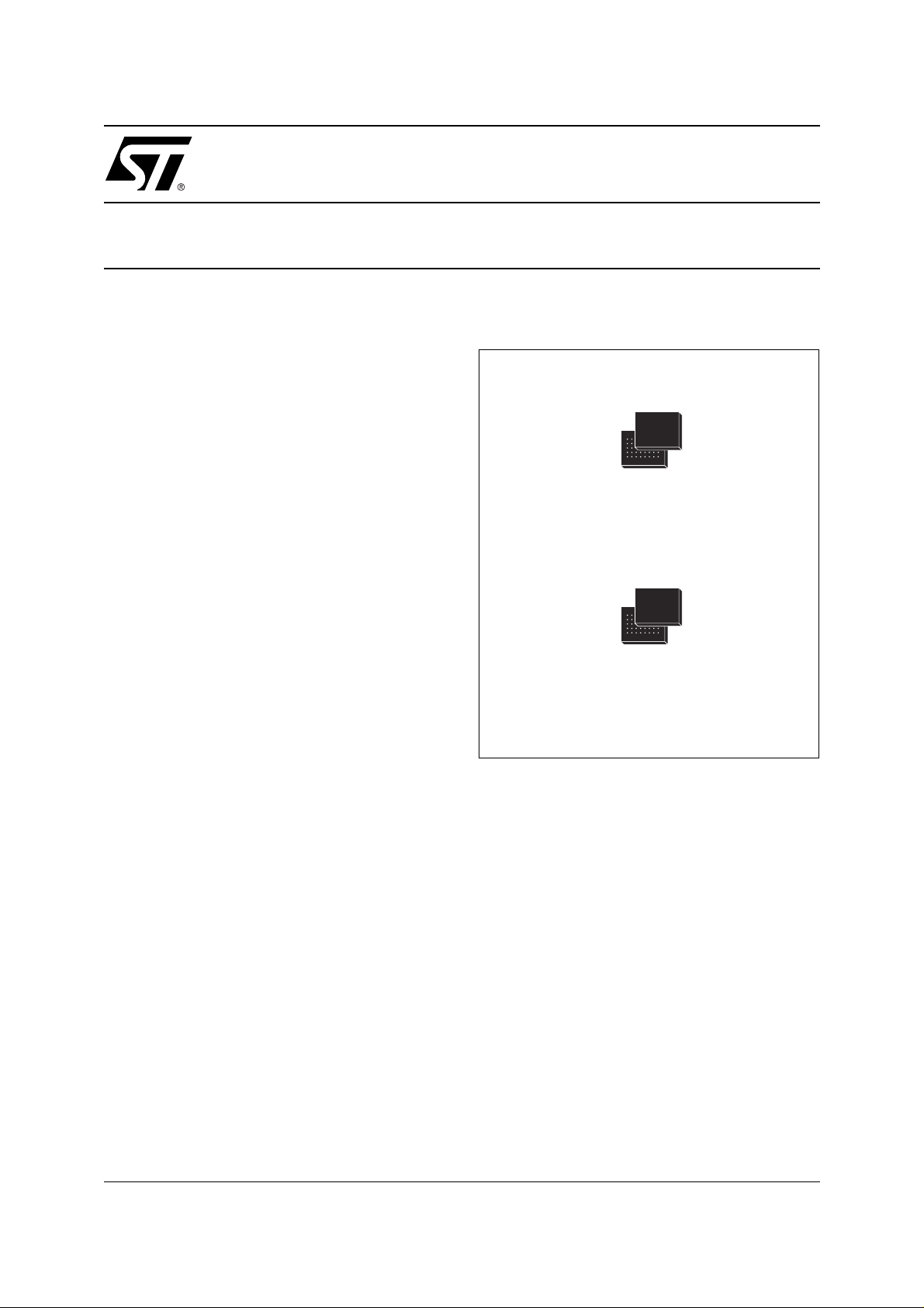
Figure 1. Packages
BGA
TFBGA48 (ZH)
8 x 10 mm
(for Engineering
Samples only)
BGA
TFBGA48 (ZB)
6.5 x 10 mm
October 2002
This is preliminary information on a new product now in development or undergoing evaluation. Details are subject to change without notice.
1/19
Page 2

M68AR024D
TABLE OF CONTENTS
SUMMARY DESCRIPTION. . . . . . . . . . . . . . . . . . . . . . . . . . . . . . . . . . . . . . . . . . . . . . . . . . . . . . . . . . . 3
Figure 2. Logic Diagram . . . . . . . . . . . . . . . . . . . . . . . . . . . . . . . . . . . . . . . . . . . . . . . . . . . . . . . . . . 3
Table 1. Signal Names . . . . . . . . . . . . . . . . . . . . . . . . . . . . . . . . . . . . . . . . . . . . . . . . . . . . . . . . . . . 3
Figure 3. TFBGA Connections (Top view through package). . . . . . . . . . . . . . . . . . . . . . . . . . . . . . . 4
Figure 4. Block Diagr am . . . . . . . . . . . . . . . . . . . . . . . . . . . . . . . . . . . . . . . . . . . . . . . . . . . . . . . . . . 5
MAXIMUM RATING. . . . . . . . . . . . . . . . . . . . . . . . . . . . . . . . . . . . . . . . . . . . . . . . . . . . . . . . . . . . . . . . . 5
Table 2. Absolute Maximum Ratings. . . . . . . . . . . . . . . . . . . . . . . . . . . . . . . . . . . . . . . . . . . . . . . . . 5
DC AND AC PARAMETERS. . . . . . . . . . . . . . . . . . . . . . . . . . . . . . . . . . . . . . . . . . . . . . . . . . . . . . . . . . 6
Table 3. Operating and AC Measurement Conditions. . . . . . . . . . . . . . . . . . . . . . . . . . . . . . . . . . . . 6
Figure 5. AC Measurement I/O Waveform . . . . . . . . . . . . . . . . . . . . . . . . . . . . . . . . . . . . . . . . . . . . 6
Figure 6. AC Measurement Load Circuit . . . . . . . . . . . . . . . . . . . . . . . . . . . . . . . . . . . . . . . . . . . . . .6
Table 4. Capacitance. . . . . . . . . . . . . . . . . . . . . . . . . . . . . . . . . . . . . . . . . . . . . . . . . . . . . . . . . . . . . 7
Table 5. DC Character i stics. . . . . . . . . . . . . . . . . . . . . . . . . . . . . . . . . . . . . . . . . . . . . . . . . . . . . . . . 7
OPERATION . . . . . . . . . . . . . . . . . . . . . . . . . . . . . . . . . . . . . . . . . . . . . . . . . . . . . . . . . . . . . . . . . . . . . . 8
Table 6. Operating Modes. . . . . . . . . . . . . . . . . . . . . . . . . . . . . . . . . . . . . . . . . . . . . . . . . . . . . . . . . 8
Read Mode . . . . . . . . . . . . . . . . . . . . . . . . . . . . . . . . . . . . . . . . . . . . . . . . . . . . . . . . . . . . . . . . . . . . 8
Figure 7. Address Controlled, Read Mode AC Waveforms. . . . . . . . . . . . . . . . . . . . . . . . . . . . . . . . 8
Figure 8. Chip Enable or Output Enable Controlled, Read Mode AC Waveforms . . . . . . . . . . . . . . 9
Figure 9. Chip Enable or UB/LB Controlled, Standby Mode AC Waveforms . . . . . . . . . . . . . . . . . . 9
Table 7. Read and Standby Mode AC Characteristics . . . . . . . . . . . . . . . . . . . . . . . . . . . . . . . . . . 10
Write Mode . . . . . . . . . . . . . . . . . . . . . . . . . . . . . . . . . . . . . . . . . . . . . . . . . . . . . . . . . . . . . . . . . . . 11
Figure 10. Write En a ble Controlled, Writ e AC Waveforms . . . . . . . . . . . . . . . . . . . . . . . . . . . . . . . 11
Figure 11. Chip Enable E1 Controlled, Write AC Waveforms . . . . . . . . . . . . . . . . . . . . . . . . . . . . . 12
Figure 12. UB/LB Controlled, Write AC Waveforms . . . . . . . . . . . . . . . . . . . . . . . . . . . . . . . . . . . . 12
Table 8. Write Mode AC Characteristics . . . . . . . . . . . . . . . . . . . . . . . . . . . . . . . . . . . . . . . . . . . . . 13
Figu r e 1 3 . E1 Con troll e d , L o w VCC D a ta Reten tion A C Wave fo rms . . . . . . . . . . . . . . . . . . . . . . . 1 4
Figu r e 1 4 . E2 Cont r o l led, Lo w VCC Data Re tenti o n AC Waveforms . . . . . . . . . . . . . . . . . . . . . . . 14
Table 9. Low VCC Data Retention Characteristics . . . . . . . . . . . . . . . . . . . . . . . . . . . . . . . . . . . . . 14
PACKAGE MECHANICAL . . . . . . . . . . . . . . . . . . . . . . . . . . . . . . . . . . . . . . . . . . . . . . . . . . . . . . . . . . 15
Figure 15. TFBGA48 6.5x10mm - 6x8 ball array, 0.75 mm pitch, Bottom View Package Outline. . 15
Table 11. TFBGA48 8x10mm - 6x8 ball array, 0.75 mm pitch, Package Mechanical Data. . . . . . . 16
PART NUMBERING . . . . . . . . . . . . . . . . . . . . . . . . . . . . . . . . . . . . . . . . . . . . . . . . . . . . . . . . . . . . . . . 17
Table 12. Ordering Information Scheme . . . . . . . . . . . . . . . . . . . . . . . . . . . . . . . . . . . . . . . . . . . . .17
REVISION HISTORY. . . . . . . . . . . . . . . . . . . . . . . . . . . . . . . . . . . . . . . . . . . . . . . . . . . . . . . . . . . . . . . 18
Table 13. Document Revision History. . . . . . . . . . . . . . . . . . . . . . . . . . . . . . . . . . . . . . . . . . . . . . .18
2/19
Page 3
SUMMARY DESCRIPTION
The M68AR024D is a 16 Mbit (16, 777,216 bit) Low
Power SRAM fabricated in STMicroelectronics advanced CMOS technology, organiz ed as 1,048,576
words by 16 bit s. The device exhi bits f ully sta tic op eration requiring no external clocks or timing
strobes.
It needs 1.65 to 1.95V supply voltage. By using the
pin all the outputs can be powered indepen-
V
CCQ
dently from the core supply voltage allowing to
drive the I/O pins down to 1.5V. V
pin can be
CCQ
tied to Vcc if the feature is not required.
This device has a standard Asynchronous SRAM
Interface. Read and Write cycles can be performed on a single byte by using UB
The device can be put into standby mode by using
/E2 pins. The same pins can be used to cas-
E1
cade more devices in order to achieve deep memory expansion.
Standby mode allows a low current consu mption,
up to 99%, by reducing internal activities.
The M68AR024D is available in TFBGA48 (0.75
mm pitch) package with industrial standard footprint.
Figure 2. Logic Diagram Table 1. Signal Names
A0-A19 Address Inputs
V
V
CC
A0-A19
W
E1
E2
UB
LB
CCQ
20
M68AR024D
G
16
DQ0-DQ15
DQ0-DQ15 Data Input/Output
, E2 Chip Enables
E1
G
W
UB
LB
V
CC
V
CCQ
V
SS
NC Not Connected Internally
Output Enable
Write Enable
Upper Byte Enable Input
Lower Byte Enable Input
Supply Voltage
I/O Supply Voltage
Ground
M68AR024D
/LB signals.
DU Don’t Use as Internally Connected
V
SS
AI05400c
3/19
Page 4
M68AR024D
Figure 3. TFBGA Connections (Top view through package)
654321
A
B
C
D
E
F
G
H
LB
DQ8
DQ9
V
SS
V
CCQ
DQ14
DQ15
UB
DQ10
DQ11
DQ12
DQ13
A19
A0G
A17
NC V
A14
A9
A1
A4 E1
A6A5
A7
A16
A15
A13
A10
A2 E2
DQ3
DQ4
DQ5
DQ0A3
DQ2DQ1
V
CC
SS
DQ6
DQ7WA12
DUA11A8A18
4/19
AI05918
Page 5
Figure 4. Block Diagram
A19
A8
ROW
DECODER
M68AR024D
MEMORY
ARRAY
DQ15
UB
E1
E2
UB
LB
Ex
W
G
DQ0
LBLB
MAXIMUM RATIN G
Stressing the device above the rating l isted in the
Absolute Maximum Ratings table m ay cause permanent damage to the device. These are stress
ratings only and operation of the device at t hese or
any other conditions ab ove those i ndicated in t he
Operating sections of this specificat ion is not im-
(8)
(8)
(8)
UB
(8)
LB
I/O CIRCUITS
COLUMN
DECODER
A0 A7
AI05924
plied. Exposure to Absolute Maximum Rating conditions for periods greater than 1 sec may affect
device reliability. Refer also to the STMicroelectronics SURE Program and other relevant quality
documents.
Table 2. Absolute Maximum Ratings
Symbol Parameter Value Unit
(1)
I
O
P
D
T
A
T
STG
V
CC
V
CCQ
(2)
V
IO
Note: 1. One output at time not to exceed 1 secon d duration.
2. Up to a m aximum operating V
Output Current 20 mA
Power Dissipation 1 W
Ambient Operating Temperature –55 to 125 °C
Storage Temperature –65 to 150 °C
Supply Voltage –0.5 to 2.5 V
I/O Supply Voltage –0.5 to 2.5 V
Input or Output Voltage
or V
CC
CCQ
–0.5 to V
of 1.95V on l y.
CCQ
+0.5
V
5/19
Page 6
M68AR024D
DC AND AC PARAMETERS
This section summarizes the operat ing and measurement conditions, as well as the DC and AC
characteristics of the device. The parameters in
the following DC and AC Characteristic tables are
derived from tests performed under the M easure-
Table 3. Operating and AC Measurement Conditions
Parameter M68AR02 4D
Supply Voltage
V
CC
I/O Supply Voltage (V
V
CCQ
Ambient Operating Temperature
CCQ
V
≤
)
CC
ment Conditions listed i n the relevant tables. Designers should check that the operating conditions
in their projects match the measurement conditions when using the quoted parameters.
1.65 to 1.95V
1.5 to 1.95V
Range 1 0 to 70°C
Range 6 –40 to 85°C
Load Capacitance (C
Output Circuit Protection Resis tance (R
Load Resistance (R
Input Rise and Fall Times
Input Pulse Voltages
Input and Output Timing Ref. Voltages
Output Transition Timing Ref. Voltages
)
L
)
1
)
2
= 0.3V
V
RL
30pF
15.3k
11.3k
1ns/V
≤
0 to V
CCQ
V
CCQ
; VRH = 0.7V
CCQ
Ω
Ω
/2
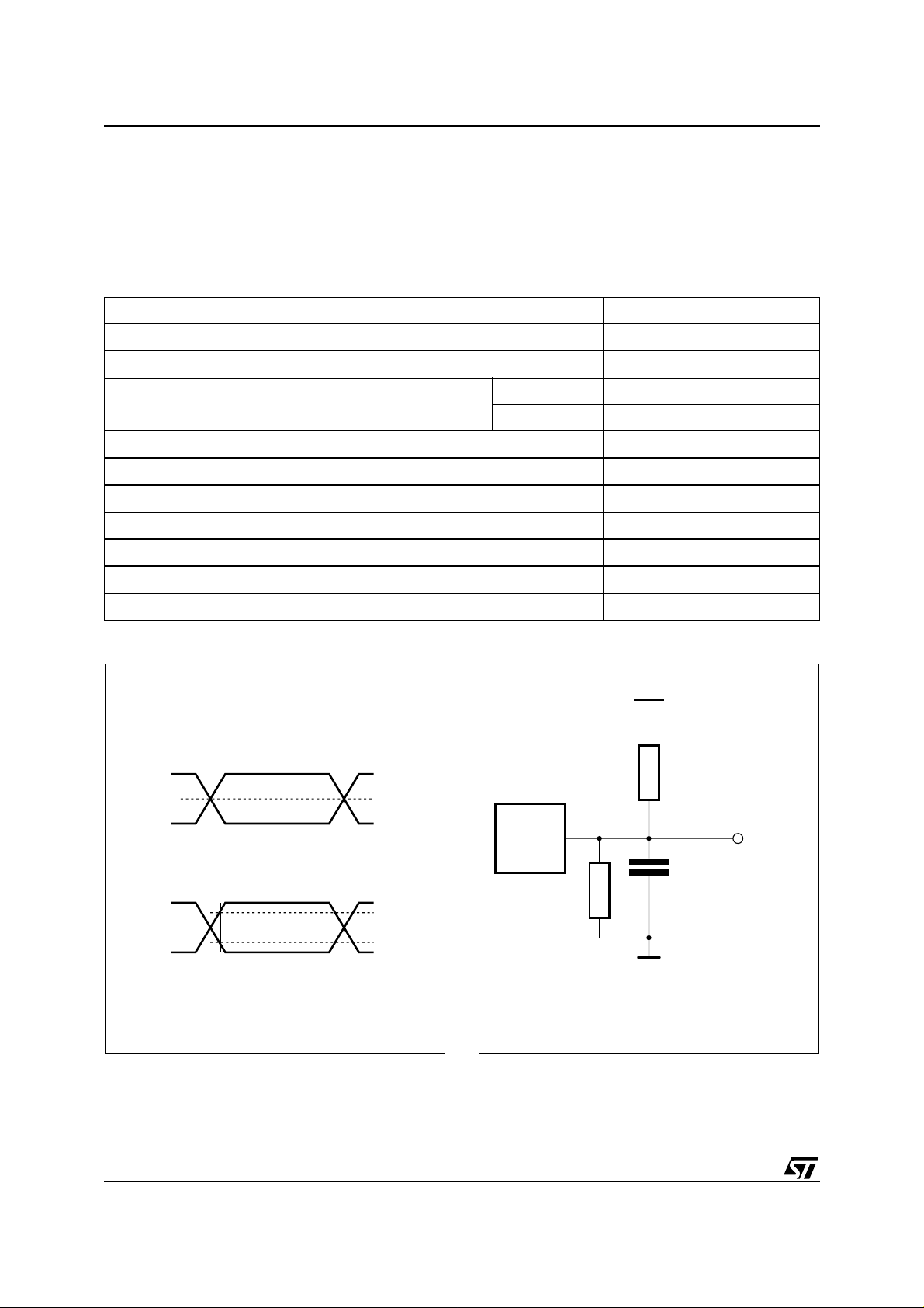
Figure 5. AC Measurement I/O Waveform Figure 6. AC Measurement Load Circuit
V
CCQ
I/O Timing Reference Voltage
R
V
CCQ
0V
I/O Transition Timing Reference Voltage
V
CCQ
0V
V
CCQ
0.7V
0.3V
AI05987
/2
CCQ
CCQ
DEVICE
UNDER
TEST
R
2
CL includes JIG capacitance
1
OUT
C
L
CCQ
6/19
AI05988
Page 7

M68AR024D
Table 4. Capacitance
Symbol
C
C
OUT
Note: 1. Sampled only, not 100% tested.
2. At T
3. Outputs desele cted.
Input Capacitance on all pins (except DQ)
IN
(3)
Output Capacitance
= 25°C, f = 1MHz, VCC = 1.8V.
A
Parameter
(1,2)
Table 5. DC Characteristics
Symbol Parameter Test Condition Min Typ Max Unit
V
= 1.95V,
(1,2)
I
CC1
(3)
I
CC2
I
LI
(4)
I
LO
I
SB
Operating Supply Current
Operating Supply Current
Input Leakage Current
Output Leakage Current
Standby Supply Current CMOS
CC
f = 1/t
I
OUT
V
CC
f = 1MHz,
I
OUT
0V ≤ V
V
0V
≤
V
CC
V
E1
≥
CCQ
E2≤ 0.2V OR
, LB ≥
UB
AVAV
= 0mA
= 1.95V,
= 0mA
V
≤
IN
≤
OUT
= 1.95V,
–0.2V OR
V
CCQ
f = 0
,
CC
V
CC
–0.2V,
Test
Condition
V
= 0V
IN
V
= 0V
OUT
Min Max Unit
6pF
8pF
525mA
3mA
–1 1 µA
–1 1 µA
115µA
V
V
V
V
Note: 1. Average AC current, cyc l ing at t
Input High Voltage
IH
Input Low Voltage –0.3 0.4 V
IL
Output High Voltage
OH
Output Low Voltage
OL
2. E1
= VIL, E2 = VIH, UB OR/AND LB = VIL, VIN = VIH OR VIL.
3. E1
≤ 0.2V or E2 ≥ V
4. Output disabled.
–0.2V, UB OR/AND LB ≤ 0.2V, V
CCQ
AVAV
minimum.
I
= –100µA V
OH
I
= 100µA
OL
≤ 0.2V or VIN≥ V
IN
V
– 0.4 V
CCQ
– 0.2
CCQ
–0.2V.
CCQ
+ 0.3
CCQ
0.2 V
V
V
7/19
Page 8

M68AR024D
OPERATION
The M68AR024D has a Chip Enable power down
feature which invokes an automatic standby mode
whenever Chip Enable is de-asserted (E1
or Chip Select is asserted (E2 = Low), or UB
= High)
/LB
are de-asserted (UB/LB = High). An Output Enable (G
) signal provides a high speed tri-state con-
Table 6. Operating Modes
Operation E1 E2 W G LB UB DQ0-DQ7 DQ8-DQ15 Power
Deselected/Standby
Deselected/Standby X
Deselected/Standby X X X X
Lower Byte Read
Lower Byte Write
Output Disabled
Upper Byte Read
Upper Byte Write
Word Read
Word Write
Note: 1. X = VIH or VIL.
V
V
V
V
V
V
V
V
X X X X X Hi-Z Hi-Z
IH
V
X X X X Hi-Z Hi-Z
IL
V
IL
V
IL
V
IL
V
IL
V
IL
V
IL
V
IL
IHVIH
IHVIL
IHVIHVIH
IHVIH
IHVIL
IHVIH
IHVIL
V
IL
X
V
IL
X
V
IL
X
trol, allowing fast read/write cycles to be achieved
with the common I/O data bus. Operational modes
are determined by device control inputs W
and UB as summarized in the Operating Modes table (see Table 6).
V
IHVIH
VILV
V
IL
X
V
IH
V
IH
V
IL
V
IL
IH
V
IH
X Hi-Z Hi-Z
V
IL
V
IL
V
IL
V
IL
Hi-Z Hi-Z
Data Output Hi-Z
Data Input Hi-Z
Hi-Z Data Output
Hi-Z Data Input
Data Output Data Output
Data Input Data Input
, E1, LB
Standby (I
Standby (I
Standby (I
Active (I
Active (I
Active (ICC)
Active (I
Active (I
Active (I
Active (I
CC
CC
CC
CC
CC
CC
SB
SB
SB
)
)
)
)
)
)
)
)
)
Read Mode
The M68AR024D , when Chip Select (E2) i s High,
is in the read mode whenever Write Enable (W
High with Output Enable (G
able (E1
) is asserted. This provides access to data
) Low, and Chip En-
) is
from eight or sixte en, depending on the status of
the signal UB
and LB, of the 16,777,216 locations
in the static memory array, specified by the 20 address inputs. Valid data will be available at the
eight or sixteen output pins within t
last stable address, providing G
Low. If Chip Enable or Output Enable access
times are n ot met, data access will be m easured
from the limiting parameter (t
rather than the address. Data out may be inde terminate at t
will always be v alid at t
Figure 7. Address Controlled, Read Mode AC Waveforms
tAVAV
A0-A19
tAVQV tAXQX
DQ0-DQ7 and/or DQ8-DQ15
Note: E1 = Low, E2 = High, G = Low, W = High, UB = Low and/or LB = Low.
VALID
, t
ELQX
DATA VALID
GLQX
and t
AVQV
after the
AVQV
is Low and E1 is
ELQV
BLQX
, t
or t
GLQV
, but data lines
AI05403
BLQV
)
8/19
Page 9

Figure 8. Chip Enable or Output Enable Controlled, Read Mode AC Waveforms
tAVAV
M68AR024D
A0-A19
E1
E2
G
DQ0-DQ15
UB, LB
Note: W rite Enable (W) = High
VALID
tAVQV tAXQX
tELQV
tELQX
tGLQV
tGLQX
VALID
tBLQV
tBLQX
tGHQZ
tBHQZ
tEHQZ
AI07730
Figure 9. Chi p E nable or UB/LB Controlled, Standby Mode AC Waveforms
E1, UB, LB
E2
I
I
CC
SB
tPU
50%
tPD
AI05990
9/19
Page 10

M68AR024D
Table 7. Read and Standby Mode AC Characteristics
Symbol Parameter
M68AR024D
Unit
70
t
AVAV
t
AVQV
t
AXQX
t
BHQZ
t
BLQV
t
BLQX
t
EHQZ
t
ELQV
t
ELQX
t
GHQZ
t
GLQV
t
GLQX
(4)
t
PD
(4)
t
PU
Note: 1. Test conditi ons assume transiti on timi ng r e f erence l evel = 0.3V
2. At any gi ven temperat ure and voltage condition, t
3. These parameters are defined as the time at which the outputs achieve the open circuit conditions and are not referenced to output
4. Tes ted initially and after any design or process changes that may affect these parameters.
Read Cycle Time Min 70 ns
Address Valid to Output Valid Max 70 ns
(1)
Data hold from address change Min 5 ns
(2, 3)
Upper/Lower Byte Enable High to Output Hi-Z Max 25 ns
Upper/Lower Byte Enable Low to Output Valid Max 70 ns
(1)
Upper/Lower Byte Enable Low to Output Transition Min 5 ns
(2, 3)
Chip Enable High to Output Hi-Z Max 25 ns
Chip Enable Low to Output Valid Max 70 ns
(1)
Chip Enable Low to Output Transition Min 5 ns
(2, 3)
Output Enable High to Output Hi-Z Max 25 ns
Output Enable Low to Output Valid Max 35 ns
(1)
Output Enable Low to Output Transition Min 5 ns
Chip Enable High to Power Down Max 0 ns
Chip Enable Low to Power Up Min 70 ns
any given de vice.
voltage lev el s.
is less than t
GHQZ
CCQ
to 0.7V
GLQX
, t
CCQ
BHQZ
.
is less than t
BLQX
and t
EHQZ
is less than t
ELQX
for
10/19
Page 11

Write Mode
The M68AR024D, when Chi p S elect (E2) i s High,
is in the Write Mode whenev er the W
Low. Either the Chip Enable Input (E1
Enable input (W
) must be de-asserted during Ad-
and E1 are
) or the Write
dress transitions for subsequent write cycles.
When E1
cycle begins on the W
or W is Low, and UB or LB is Low, write
or E1 falling edge. When E1
and W are Low, and UB = LB = High, write cycle
begins on the first falling edge of UB
or LB. Therefore, address setup time is referenced to Write Enable, Chip Enables and UB
t
respectively, and is det ermined by the latter
AVBL
/LB as t
AVWL
, t
AVEL
and
occurring falling edge.
The Write cycle can be terminated by the earlier
rising edge of E1
If the Output is enabled (E1
Low, LB
puts to high impedance within t
edge. Care must be taken to avoid bus contention
in this type of operation. Data input must be valid
for t
DVWH
or for t
before the rising edge of UB/LB, whichever
VBH
occurs first, and remain valid for t
t
BHDX
Figure 10. Write Enable Controlled, Write AC Waveforms
tAVAV
M68AR024D
, W, UB and LB.
= Low, E2 = High, G =
or UB = Low), then W will return the out-
of its fall ing
WLQZ
before the rising edge of Write Enable,
before the rising edge of E1 or for t
DVEH
, t
respectively.
WHDX
EHDX
D-
and
A0-A19
E1
E2
W
DQ0-DQ15
UB, LB
tAVEL
tAVWL
tWLQZ
VALID
tAVWH
tELWH
tWLWH
tBLBH
tWHAX
tWHQX
tWHDX
DATA INPUT
tDVWH
AI05991
11/19
Page 12

M68AR024D
Figu r e 1 1 . C h i p Enab le E1 Controlle d, Write AC Waveforms
tAVAV
A0-A19
E1
E2
W
DQ0-DQ15
UB, LB
Figure 12. UB
VALID
tAVEH
tAVEL
tAVWL
tWLEH
tBLBH
/LB Controlled, Write AC Waveforms
tELEH
tEHAX
tEHDX
DATA INPUT
tDVEH
AI05992
tAVAV
A0-A19
E1
E2
tAVWL
W
tWLQZ tBHDX
(1)
DQ0-DQ15
UB, LB
Note: 1. During this period DQ0-DQ15 are in output s tate and input signals shoul d not be appli ed.
DATA
tAVBL
VALID
tAVBH
tWLBH
DATA INPUT
tDVBH
tBLBH
tBHAX
AI05993
12/19
Page 13

Table 8. Write Mode AC Characteristics
Symbol Parameter
M68AR024D
M68AR024 D
Unit
70
t
AVAV
t
AVBH
t
AVBL
t
AVEH
t
AVEL
t
AVWH
t
AVWL
t
BHAX
t
BHDX
t
BLBH
t
BLEH
t
BLWH
t
DVBH
t
DVEH
t
DVWH
t
EHAX
t
EHDX
t
ELBH
t
ELEH
t
ELWH
t
WHAX
t
WHDX
t
WHQX
t
WLBH
t
WLEH
t
WLQZ
t
WLWH
Note: 1. At any given temperature and v ol tage condit i on, t
2. These parameters are defined as the time at which the outputs achieve the open circuit conditions and are not referenced to output
voltage lev el s.
Write Cycle Time Min 70 ns
Address Valid to LB, UB High Min 60 ns
Addess Valid to LB, UB Low Min 0 ns
Address Valid to Chip Enable High Min 60 ns
Address valid to Chip Enable Low Min 0 ns
Address Valid to Write Enable High Min 60 ns
Address Valid to Write Enable Low Min 0 ns
LB, UB High to Address Transition Min 0 ns
LB, UB High to Input Transition Min 0 ns
LB, UB Low to LB, UB High Min 60 ns
LB, UB Low to Chip Enable High Min 60 ns
LB, UB Low to Write Enable High Min 60 ns
Input Valid to LB, UB High Min 30 ns
Input Valid to Chip Enable High Min 30 ns
Input Valid to Write Enable High Min 30 ns
Chip Enable High to Address Transition Min 0 ns
Chip enable High to Input Transition Min 0 ns
Chip Enable Low to LB, UB High Min 60 ns
Chip Enable Low to Chip Enable High Min 60 ns
Chip Enable Low to Write Enable High Min 60 ns
Write Enable High to Address Transition Min 0 ns
Write Enable High to Input Transition Min 0 ns
(1)
Write Enable High to Output Transition Min 5 ns
Write Enable Low to LB, UB High Min 60 ns
Write Enable Low to Chip Enable High Min 60 ns
(1, 2)
Write Enable Low to Output Hi-Z Max 20 ns
Write Enable Low to Write Enable High Min 50 ns
WHQZ
is less than t
for any given device.
WLQX
13/19
Page 14

M68AR024D
Figure 13. E1 Controlled, Low VCC Data Retention AC Waveforms
1.95V
VCC 1.65V
VDR> 1.0V
E1
Figure 14. E2 Controlled, Low V
1.95V
VCC 1.65V
VDR> 1.0V
E2
DATA RETENTION MODE
tCDR
E1 ≥ VDR– 0.2V
Data Retention AC Waveforms
CC
DATA RETENTION MODE
tCDR
E2 ≤ 0.2V
tR
AI05855
tR
AI05875
Table 9. Low V
Data Retention Characteristics
CC
Symbol Parameter Test Condition Min Typ Max Unit
V
CCQ
E2 ≤ 0.2V OR
V
–0.2V,
CCQ
–0.2V OR
0.5 5 µA
I
CCDR
(1)
Supply Current (Data Retention)
V
= 1.0V, E1 ≥
CC
UB
, LB ≥
f=0
Chip deselected to Data
(2)
t
CDR
t
R
V
DR
Retention Time
(2)
Operation Recovery Time
(1)
Supply Voltage (Data Retention)
V
E1
≥
CCQ
E2 ≤ 0.2V OR
UB
, LB ≥
–0.2V OR
V
CCQ
–0.2V,
0ns
t
AVAV
1.0 V
f=0
Note: 1. All other Inputs at V
2. Tes ted initially and after any design or process changes that may affect these parameters.
3. No input may exceed V
≥ V
CCQ
CC
–0.2V or V
+0.2V.
IH
≤ 0.2V.
IL
t
is Read c ycle time.
AVAV
ns
14/19
Page 15

M68AR024D
PACKAGE MECHANICAL
Figure 15. TFBGA48 6.5x10mm - 6x8 ball array, 0.75 mm pitch, Bottom View Package Outline
D
D1
SD
FD
FE
SE
E1E
BALL "A1"
Note: Drawing is not to scale.
e
A
b
e
ddd
A2
A1
BGA-Z30
Table 10. TFBGA48 6.5x10mm - 6x8 ball array, 0.75 mm pitch, Package Mechanical Data
Symbol
Typ Min Max Typ Min Max
A 1.200 0.0472
A1 0.300 0.400 0.0118 0.0157
A2 0.790 0.03 11
b 0.350 0.45 0 0.0138 0.0177
D 6.500 6.400 6.600 0.2559 0.2520 0.2598
D1 3 .750 – – 0.14 76 – –
ddd 0.100 0.0039
E 10.000 9.900 10.100 0.3937 0.3898 0.3976
E1 5.250 – – 0.2067 – –
millimeters inches
e 0.750 – – 0.0295 – –
FD 0.875 – – 0.0344 – –
FE 3 .125 – – 0.12 30 – –
SD 0.375 – – 0.0148 – –
SE 0.375 – – 0.0148 – –
15/19
Page 16

M68AR024D
Figure 16. TFBGA48 8x10mm - 6x8 ball array, 0.75 mm pitch, Bottom View Packag e Outl ine
D
BALL "A1"
Note: Drawing is not to scale.
E1E
FD
FE
A
D1
SD
SE
eb
A2
A1
ddd
BGA-Z28
Table 11. TFBGA48 8x10mm - 6x8 ball array, 0.75 mm pitch, Package Mech anical Data
Symbol
Typ Min Max Typ Min Max
A 1.200 0.0472
A1 0.260 0.0 102
A2 0.900 0.0354
b 0.350 0.45 0 0.0138 0.0177
D 8.000 7.900 8.100 0.3150 0.3110 0.3189
D1 3 .750 – – 0.14 76 – –
ddd 0.100 0.0039
E 10.000 9.900 10.100 0.3937 0.3898 0.3976
E1 5.250 – – 0.2067 – –
e 0.750 – – 0.0295 – –
FD 2.125 – – 0.0837 – –
FE 2 .375 – – 0.09 35 – –
SD 0.375 – – 0.0148 – –
SE 0.375 – – 0.0148 – –
millimeters inches
16/19
Page 17

PART NUMBERING
Table 12. Ordering Information Scheme
Example: M68AR016 D N 70 ZB 6 T
Device Type
M68
Mode
A = Asynchronous
Operating Voltage
R = 1.65 to 1.95V
Array Organization
024 = 16 Mbit (1M x16)
Option 1
D = 2 Chip Enable; Write and Standby from UB
Option 2
N = N-Die
and LB
M68AR024D
Speed Class
70 = 70 ns
Package
ZH = TFBGA48: 0.75 mm pitch (8x10mm)
ZB = TFBGA48: 0.75 mm pitch (6.5x10mm)
Operative Temperature
1 = 0 to 70°C
6 = –40 to 85 °C
Shipping
T = Tape & Reel Packing
Note: 1. This package is ava ilable for Engi neering Samples only.
(1)
17/19
Page 18

M68AR024D
REVISION HIST ORY
Table 13. Document Revision History
Date Version Revision Details
July 2001 -01 First Issue
Table of Contents added
24-Oct-2001 -02
07-Nov-2001 -03 Voltage range extended up to 2.2V
19-Feb-2002 -04 Document totally revised
Block Diagram added, Data Retention AC Waveforms clarified
Package Mechanical Data and Drawing added
12-Mar-2002 -05
20-Mar-2002 -06 TFBGA 6.5x10 package added
19-Apr-2002 -07
02-Oct-2002 7.1
04-Oct-2002 7.2 Document status changed from Target Specification to Preliminary Data.
09-Oct-2002 7.3 Part number modified.
Features Summary clarified
Tables 2, 3, 4, 5, 6, 7, 8 and 9 clarified
Figures 8, 10, 11 and 12 clarified
Chip Enable Controlled, Low V
and 14)
Revision numbering modified: a minor revision will be indicated by incrementing the
digit after the dot, and a major revision, by incrementing the digit before the dot
(revision version 07 equals 7.0).
Part number changed.
Data Retention AC Wavef orms clarified (Figures 13
CC
18/19
Page 19

M68AR024D
Information furnished is believed to be accurate an d rel i able. However, STMicroelectro ni cs assumes no responsibilit y for the cons equences
of use of such information nor for any infringement of patents or other rights of third parties which may result from its use. No license is granted
by implic ation or otherwise under any patent or patent rights of STMi croelectr onics. Specifications mentioned in th i s publication are subject
to change without notice. This publication supersedes and replaces all information previously supplied. STMicroelectronics products are not
authoriz ed for use as critical comp onents in lif e support devi ces or systems wi thout exp ress written approval of STM i croelect ronics.
The ST logo is registered trademark of STMicroelectronics
All other na m es are the prop erty of their respectiv e owners.
© 2002 STMicroelectronics - All Rights Reserved
Australi a - Brazil - Canada - China - F i nl and - Franc e - Germany - H ong Kong - India - Israel - Ital y - Japan - Mal aysia - Malta -
Morocc o - Singapore - S pai n - Sweden - Swi tzerland - United Kingdom - United States
STMicroelectronics GROUP OF COMPANIES
www.st.com
19/19
 Loading...