

Page 1
MITSUBISHI <DIGITAL ASSP>
M66850J/FP, M66851J/FP
M66852J/FP, M66853J/FP
SRAM TYPE FIFO MEMORY
DESCRIPTION
M66850/851/852/853 are very high-speed and clock synchronous
FIFO(First-In,First-Out) memories fabricated by high-speed CMOS
technology.
These FIFOs are applicable for a data buffer as networks and
communications.
The write operation is controlled by a write clock pin(WCLK) and
two write enable pins(WEN1,WEN2).
Data present at the data input pins(D0-D8) is written into the
Synchronous FIFO on every rising write clock edge when the
device is enabled for writing.
The read operation is controlled by a read clock pin(RCLK) and
two read enable pins(REN1,REN2).
Data is read from the Synchronous FIFO on every rising read clock
edge when the device is enabled for reading. An output enable
pin(OE) controls the states of the data output pins(Q0-Q8).
MITSUBISHI FIFOs have four flags (EF,FF,PAE,PAF). The empty
flag EF and the full flag FF are fixed flags. The almost empty flag
PAE and the almost full flag PAF are programmable flags. The
programmable flag offset is initiated by the load pin(LD).
FEATURES
• Memory configuration 64words x 9bits (M66850J/FP)
256words x 9bits (M66851J/FP)
512words x 9bits (M66852J/FP)
1024words x 9bits (M66853J/FP)
• Write and Read Clocks can be independent
• Advanced CMOS technology
• Programmable Almost-Empty and Almost-Full flags
• High-speed : 25ns cycle time
• Package Available :
32-pin Pastic Leaded Chip Carrier(PLCC)
32-pin Low profile Quad Flat Package(LQFP)
APPLICATION
• Data Buffer for networks communications.
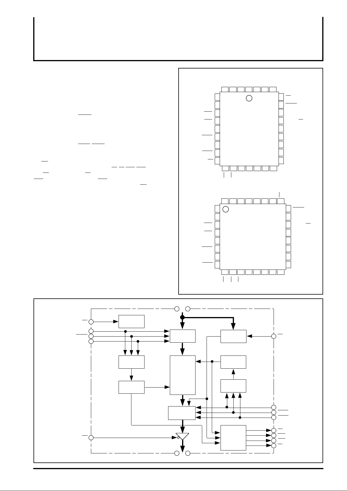
PIN CONFIGURATION (TOP VIEW)
D4D5D6D7D8
D2
D3
4
5
D1
6
D0
7
PAF
8
PAE
9
GND
10
REN1
11
RCLK
12
REN2
13
OE
14
EF
Outline 32P0(M66850 – 853J)
D2
32
1
D1
2
D0
3
PAF
4
PAE
5
GND
6
REN1
7
RCLK
REN2
8
9
OE
Outline 32P6B(M66850 – 853FP)
1
3
2
32
15
16
17
18
FF
Q0Q1Q2
D4D5D6D7D8
D3
31
30
29
28
11
10
12
13
FF
Q0Q1Q2
EF
31
19
Q3
27
14
30
20
Q4
26
15
Q3
29
RS
28
WEN1
27
WCLK
26
WEN2/LD
25
V
24
Q8
23
Q7
22
Q6
21
Q5
RS
25
16
Q4
CC
24
WEN1
23
WCLK
22
WEN2/LD
21
V
20
Q8
19
Q7
18
Q6
17
Q5
CC
BLOCK DIAGRAM
WCLK
WEN1
WEN2
RS
OE
RESET
LOGIC
WRITE
CONTROL
WRITE
POINTER
D0-D8
–
INPUT
REGISTER
MEMORY
ARRAY
OUTPUT
REGISTER
–
Q0-Q8
OFFSET
REGISTER
READ
POINTER
READ
CONTROL
FLAG
LOGIC
LD
RCLK
REN1
REN2
EF
PAE
PAF
FF
1
Page 2

MITSUBISHI <DIGITAL ASSP>
M66850J/FP, M66851J/F P
M66852J/FP, M66853J/F P
SRAM TYPE FIFO MEMORY
PIN and SIGNAL DESCRIPTIONS
•VCC
One+5 volt power supply pin.
• GND
One 0 volt ground pin.
• RS : Reset(INPUT)
When RS is set LOW, internal read and write pointers are set to
the first physical location,the output register is initialized to LOW,
FF and PAF are set HIGH, EF and PAE are set LOW.
A reset is required after power-up before a write operation.
• WCLK : Write Clock(INPUT)
Data present on D0-D8 is written into the FIFO on the rising edge
of WCLK when the FIFO is enabled for writing.
• RCLK : Read Clock(INPUT)
Data is read from the FIFO on the rising edge of RCLK when the
FIFO is enabled for reading.
• WEN1 : Write Enable1(INPUT)
If the FIFO is configured to allow loading of the offset registers,
WEN1 is the only the write enable. When WEN1 is LOW, data on
D0-D8 is written to the FIFO on the rising edge of WCLK.
If the FIFO is configured to have two writeenables, data on D0D8 is written to the FIFO on the rising edge of WCLK when
WEN1 is LOW and WEN2 is High. But if the FF is LOW, data on
D0-D8 will not be written to the FIFO.
• EF : Empty Flag(OUTPUT)
The Empty flag goes LOW when the read pointer is equal to the
write pointer.
When EF is LOW, the FIFO is empty and further data reads from
the data output are inhibited.
EF is synchronized to the rising edge of RCLK.
• PAE : Programmable Almost-Empty Flag(OUTPUT)
When PAE is LOW, the FIFO is almost empty based on the
offset. The default offset is Empty+7. PAE is synchronized to the
rising edge of RCLK.
• FF : Full Flag(OUTPUT)
When FF is LOW, the FIFO is full and further data writes into the
data input are inhibited.
The Full Flag goes LOW when the FIFO is full of data.
FF is synchronized to the rising edge of WCLK.
• PAF : Programmable Almost-Full Flag(OUTPUT)
When PAF is LOW, the FIFO is almost full based on the offset.
The default offset is Full-7. PAF is synchronized to the rising
edge of WCLK.
• WEN2/LD : Write Enable2/Load(INPUT)
The function of this signal is defined at reset.
If WEN2/LD is HIGH at reset, this signal functions as a second
write enable(WEN2). If WEN2/LD is LOW at reset, this signal
functions as a control to load and read the offset register.
If the FIFO is configured to have two write enables, data on D0D8 is written to the FIFO on the rising edge of WCLK when
WEN1 is LOW and WEN2 is High. But if the FF is LOW, data on
D0-D8 will not be written to the FIFO.
If the FIFO is configured to have programmable flags, it is
possible to write and read from the offset registers. There are
four 9-bit offset registers. Two are used to control the
programmable Almost-Empty Flag
programmable Almost-Full Flag.
Data on D0-D8 is written to an offset register on the rising edge
of WCLK when WEN1 is LOW and LD is LOW. Data on D0 – D8
is written to the offset registers in the following order :
PAE LSB, PAE MSB, PAF LSB, PAF MSB.
• REN1, REN2 : Read Enable(INPUT)
Data is read from the FIFO and presented Q0-8 on the rising
edge of RCLK, when REN1 and REN2 are LOW and output port
is enabled.
If either Read Enable is HIGH,the output register holds the
previous data.
When the FIFO is empty, the Read Enable signals are ignored.
• OE : Output Enable(INPUT)
When OE is LOW, the output port Q0-8 is enabled for output.
When OE is HIGH, the output port Q0-8 is placed in a high
impedance state.
and
two are used to control the
• D0-8 : Data Input(INPUT)
D0-8 is the 9-bit data input port.
• Q0-8 : Data Output(OUTPUT)
Q0-8 is the 9-bit data Output port.
2
Page 3

OFFSET FLAG
MITSUBISHI <DIGITAL ASSP>
M66850J/FP, M66851J/F P
M66852J/FP, M66853J/F P
SRAM TYPE FIFO MEMORY
LD WEN1 WCLK SELECTION
0 0 Empty Offset (LSB)
Empty Offset (MSB)
Full Offset (LSB)
Full Offset (MSB)
0 1 No Operation
1 0 Write into FIFO
1 1 No Operation
Figure 1. Write Offset Register
M66850J(64X9-bit) OFFSET REGISTERS
876543210
PAE LSB
PAE MSB
PAF LSB
PAF MSB
M66851J(256X9-bit) OFFSET REGISTERS
PAE LSB
PAE MSB
PAF LSB
PAF MSB
E0/F0 are the least significant bits.
X=Don't Care.
X X X E5E4E3E2E1E0
Default Value 007H
XXXXXXXXX
X X X F5F4F3F2F1F0
Default Value 007H
XXXXXXXXX
876543210
XE7E6E5E4E3E2E1E0
Default Value 007H
XXXXXXXXX
XF7F6F5F4F3F2F1F0
Default Value 007H
XXXXXXXXX
LD REN1 REN2 RCLK SELECTION
0 0 0 Empty Offset (LSB)
Empty Offset (MSB)
Full Offset (LSB)
Full Offset (MSB)
0 0 1
1 0 No Operation
1 1
1 1 0 Read from FIFO
1 0 1
1 0 No Operation
1 1
Figure 2. Read Offset Register
M66852J(512X9-bit) OFFSET REGISTERS
876543210
PAE LSB
PAE MSB
PAF LSB
PAF MSB
M66853J(1024X9-bit) OFFSET REGISTERS
PAE LSB
PAE MSB
PAF LSB
PAF MSB
XE7E6E5E4E3E2E1E0
Default Value 007H
XXXXXXXXE8
Default Value 0
XF7F6F5F4F3F2F1F0
Default Value 007H
XXXXXXXXF8
Default Value 0
876543210
XE7E6E5E4E3E2E1E0
Default Value 007H
XXXXXXXE9E8
Default Value 0 0
XF7F6F5F4F3F2F1F0
Default Value 007H
XXXXXXXF9F8
Default Value 0 0
Figure 3. Offset Regigter Location
3
Page 4

ABSOLUTE MAXIMUM RATINGS
MITSUBISHI <DIGITAL ASSP>
M66850J/FP, M66851J/F P
M66852J/FP, M66853J/F P
SRAM TYPE FIFO MEMORY
Symbol
Vcc
VI
VO
Pd
Tstg
Note : 450mW(32P6B), 550mW(32P0)
Supply voltage
Input voltage
Output voltage
Maximum power dissipation
Storage temperature
Parameter Conditions
A value based on GND pin
Ta=70˚C
-0.5 – +7.0
-0.3 – V
-0.3 – V
RECOMMENDED OPERATING CONDITIONS
Symbol
Vcc Supply voltage 4.5
GND
Topr
Supply voltage
Operating ambient temperature
Min.
0
Limits
Typ.
5
0
Max.
5.5
70
UnitParameter
V
V
˚C
DC ELECTRICAL CHARACTERISTICS (Ta=0 – 70˚C, Vcc=5V±10%, GND=0V)
Symbol Test conditions UnitParameter
IH
V
V
IL
VOH
VOL
IIH
IIL
I
OZH
IOZL
I
CC1
ICC2
CI
CO Off state output capacitance
"H"input voltage
"L"input voltage
"H"output voltage
"L"output voltage
"H"input current
"L"input current
Off state "H"output current
Off state "L"output current
Operating power supply current
Power supply current (Static)
Input capacitance
I
OH =-1mA
I
OL =8mA
V
I =VCC, Any input
V
I = GND, Any input
VO =VCC
VO =GND
V
I =VCC or GND, f = 40MHz, Outputs are open
V
I =VCC or GND, Outputs are open
f = 1MHz
f = 1MHz
Ratings
CC+0.5
CC+0.5
Note
-65 – 150
Min. Typ. Max.
2.0
2.4
Unit
mW
Limits
V
V
V
˚C
0.8
0.4
1.0
-1.0
5.0
-5.0
70
500
10 pF
15
V
V
V
V
µ
µ
µ
µ
mA
µ
pF
A
A
A
A
A
4
Page 5
M66850J/FP, M66851J/F P
M66852J/FP, M66853J/F P
SWITCHING CHARACTERISTICS (Ta=0 – 70˚C, Vcc=5V±10%, GND=0V)
Symbol UnitParameter
AC
t
tWFF
REF
t
tPAF
tPAE
tOE
tOLZ
tOHZ
tRSF
TIMING CONDITIONS (Ta=0 – 70˚C, Vcc=5V±10%, GND=0V)
Symbol UnitParameter
tCLK
tCLKH
tCLKL
tDS
tDH
tENS
tENH
tRS
tRSS
tRSR
tSKEW1
tSKEW2
Data Access Time
Write Clock to Full Flag
Read Clock to Empty Flag
Write Clock to Almost-Full Flag
Read Clock to Almost-Empty Flag
Output Enable to Output Valid
Output Enable to Output in Low-Z
Output Enable to Output in High-Z
Reset to Flag and Output Valid time
Clock Cycle Time
Clock Pulse Width HIGH
Clock Pulse Width LOW
Data Setup Time
Data Hold Time
Enable Setup Time
Enable Hold Time
Reset Pulse Width
Reset Setup Time
Reset Recovery Time
Skew time between Read Clock and Write Clock for Empty Flag and Full Flag
Skew time between Read Clock and Write Clock for Almost-Empty Flag and Almost-Full
Flag
MITSUBISHI <DIGITAL ASSP>
SRAM TYPE FIFO MEMORY
Limits
Min. Typ. Max.
3
3
0
3
Limits
Min. Typ. Max.
25
10
10
6
1
6
1
25
25
25
10
40
15
15
15
15
15
13
13
25
ns
ns
ns
ns
ns
ns
ns
ns
ns
ns
ns
ns
ns
ns
ns
ns
ns
ns
ns
ns
ns
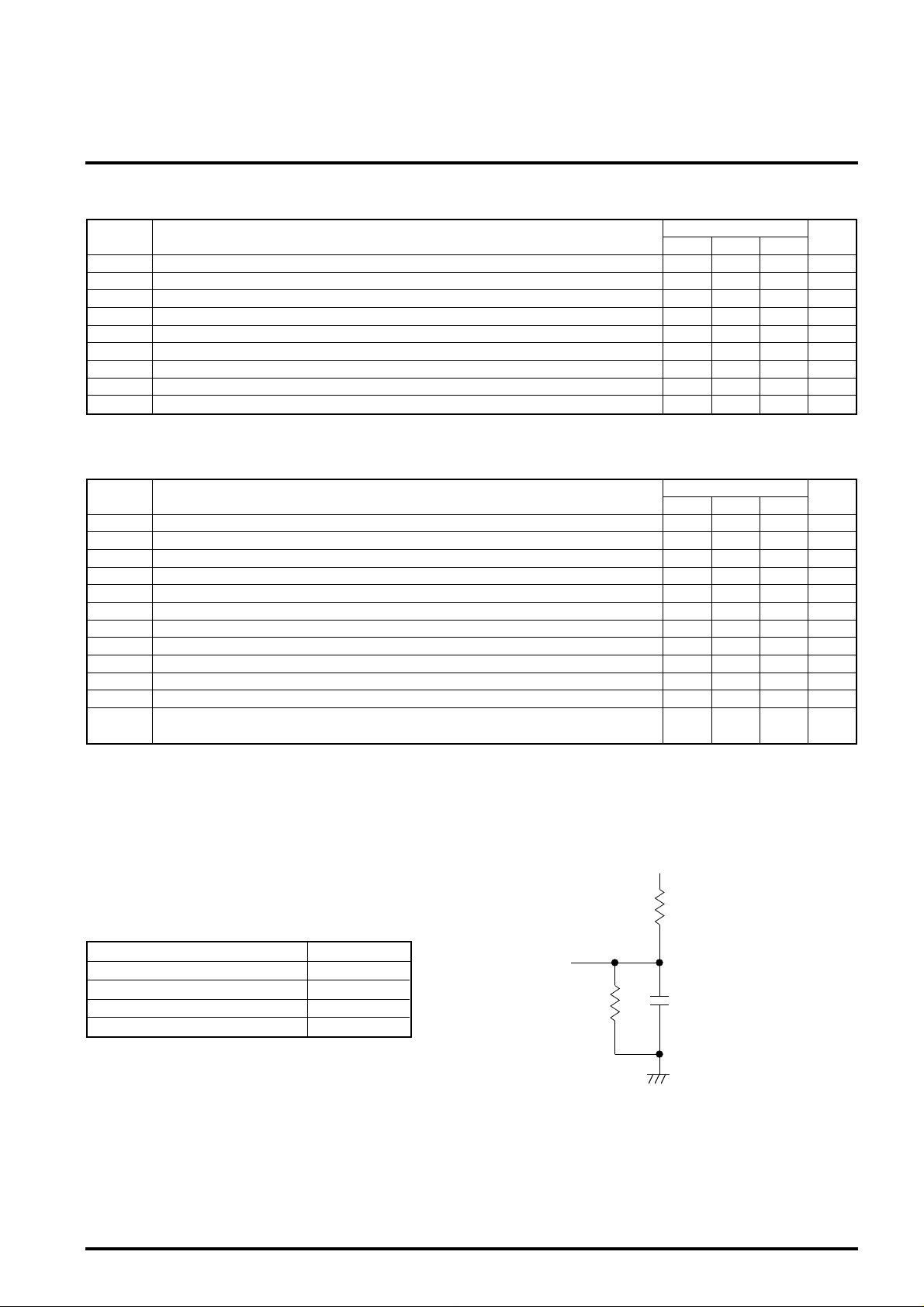
AC TEST CONDITIONS
In Pulse Levels GND – 3.0V
Input Rise/Fall Times 3ns
Input Timing Reference Levels 1.5V
Output Reference Levels 1.5V
Output Load See Figure 4
5.0V
1.1kΩ
D.U.T.
680Ω
Figure 4. Output Load
Including Test board and scope capacitances.
30pF
5
Page 6

• Reset Timing
MITSUBISHI <DIGITAL ASSP>
M66850J/FP, M66851J/F P
M66852J/FP, M66853J/F P
SRAM TYPE FIFO MEMORY
tRS
RS
REN1
REN2
WEN1
WEN2/LD
EF, PAE
FF, PAE
Q0-8
(1)
t
RSF
tRSF
tRSF
tRSS
tRSS
tRSS
tRSR
RSR
t
tRSR
OE=1
OE=0
NOTE :
1. If during reset WEN2/LD is HIGH,this signal functions as a second enable(WEN2).
If during reset WEN2/LD is LOW,this signal functions as an offset register.
6
Page 7

• Write Cycle Timing
WCLK
D0-D8
WEN1
tCLKH
tCLK
DATA IN VALID
tCLKL
tENS
MITSUBISHI <DIGITAL ASSP>
M66850J/FP, M66851J/F P
M66852J/FP, M66853J/F P
SRAM TYPE FIFO MEMORY
tDH
tDS
tENH
NO OPERATION
WEN2/(if Applicable)
RCLK
REN1
REN2
NOTE :
1. t
SKEW1 is the minimum time between a rising RCLK edge and a rising WCLK edge for FF to change during the current clock cycle.
If the time between the rising edge of RCLK and the rising edge of WCLK is less than t
the next WCLK edge.
FF
tSKEW1
(1)
tWFF
NO OPERATION
tWFF
SKEW1, then FF may not change state untill
7
Page 8

• Read Cycle Timing
RCLK
tCLKH
MITSUBISHI <DIGITAL ASSP>
M66850J/FP, M66851J/F P
M66852J/FP, M66853J/F P
SRAM TYPE FIFO MEMORY
tCLK
tCLKL
REN1
REN2
Q0-8
OE
WCLK
EF
tENS
tENH
NO OPERATION
tREF
tAC
OLZ
t
tOE
VALID DATA
t
OHZ
(1)
tSKEW1
tREF
WEN1
WEN2
NOTE :
1. t
SKEW1 is the minimum time between a rising RCLK edge and a rising WCLK edge for EF to change during the current clock
cycle. If the time between the rising edge of RCLK and the rising edge of WCLK is less than t
change state untill the next RCLK edge.
8
SKEW1, then EF may not
Page 9

• First Data Word Latency Timing
WCLK
MITSUBISHI <DIGITAL ASSP>
M66850J/FP, M66851J/F P
M66852J/FP, M66853J/F P
SRAM TYPE FIFO MEMORY
tDS
D0-D8
WEN1
WEN2
(If Applicable)
RCLK
EF
REN1
REN2
tENS
tSKEW1
D0 (First Valid)
(1)
tFRL
tREF
D1 D2 D3
tAC
tAC
Q0-Q8
tOLZ
OE
NOTE :
1. When t
SKEW1≥minimum specification, tFRL maximum=tCLK+tSKEW1.
When t
SKEW1≤minimum specification, tFRL maximum=2tCLK+tSKEW1 or tCLK+tSKEW1.
tOE
D0
D1
9
Page 10

• Full Flag Timing
MITSUBISHI <DIGITAL ASSP>
M66850J/FP, M66851J/F P
M66852J/FP, M66853J/F P
SRAM TYPE FIFO MEMORY
WCLK
D0-D8
WEN1
WEN2
(If Applicable)
FF
NO WRITE
tSKEW1
tWFF
tDS
tWFF
NO WRITE
tSKEW1
tDS
DATA WRITE
tWFF
RCLK
REN1
REN2
OE
Q<8:0>
tENH
tENS
tAC
LOW
DATA IN OUTPUT REGISTER DATA READ NEXT DATA READ
tENS
tENH
tAC
10
Page 11

• Empty Flag Timing
WCLK
MITSUBISHI <DIGITAL ASSP>
M66850J/FP, M66851J/F P
M66852J/FP, M66853J/F P
SRAM TYPE FIFO MEMORY
D0-D8
WEN1
WEN2
(If Applicable)
RCLK
EF
tDS
DATA WRITE1
tENS
tENS
tENH
tENH
SKEW1
t
tFRL
(1)
tREF
tREF
tDS
tENS
tENS
DATA WRITE2
tENH
tENH
tSKEW1
tFRL
(1)
tREF
REN1
REN2
OE
Q0-Q8
NOTE :
1. When t
When t
LOW
tAC
DATA IN OUTPUT REGISTER
SKEW1≥minimum specification, tFRL maximum=tCLK+tSKEW1.
SKEW1≤minimum specification, tFRL maximum=2tCLK+tSKEW1 or tCLK+tSKEW1.
DATA READ
11
Page 12

• Programmable Full Flag Timing
MITSUBISHI <DIGITAL ASSP>
M66850J/FP, M66851J/F P
M66852J/FP, M66853J/F P
SRAM TYPE FIFO MEMORY
WCLK
WEN1
WEN2
(If Applicable)
PAF
RCLK
tCLKH t CLKL
tENS tENH
tENS
Full-(m+1) words in FIFO
tENH
(1)
(4)
tPAF
Full-m words
(2)
in FIFO
t
SKEW2
(3)
tPAF
tENH
tENS
REN1
REN2
NOTES :
1. PAF offset=m.
2. 64-m words in for M66850, 256-m words in for M66851,512-m words in for M66852, 1024-m words in for M66853.
3. t
SKEW2 is the minimum time between a rising RCLK edge and a rising WCLK edge for PAF to change during that clock cycle.
If the time between the rising edge of RCLK and the rising edge of WCLK is less than t
untill the next rising edge of WCLK.
4. If a write is performed on this rising edge of the write clock,there will be Full-(m-1) words in the FIFO when PAF goes LOW.
SKEW2, then PAF may not change state
12
Page 13

• Programmable Empty Flag Timing
tCLKH tCLKL
WCLK
WEN1
WEN2
(If Applicable)
tENS
tENS
MITSUBISHI <DIGITAL ASSP>
M66850J/FP, M66851J/F P
M66852J/FP, M66853J/F P
SRAM TYPE FIFO MEMORY
tENH
tENH
PAE
RCLK
REN1
REN2
NOTES :
1. PAF offset=m.
2. t
If the time between the rising edge of WCLK and the rising edge of RCLK is less than t
untill the next rising edge of RCLK.
3. If a read is performed on this rising edge of the read clock, there will be Empty+(n-1) words in the FIFO when PAE goes LOW.
n words in FIFO
SKEW2 is the minimum time between a rising WCLK edge and a rising RCLK edge for PAE to change during that clock cycle.
(1)
SKEW2
t
(2)
tPAE
n+1 words in FIFO
tENS
tENH
SKEW2, then PAE may not change state
tPAE
(3)
13
Page 14

• Write Offset Registers Timing
WCLK
MITSUBISHI <DIGITAL ASSP>
M66850J/FP, M66851J/F P
M66852J/FP, M66853J/F P
SRAM TYPE FIFO MEMORY
tCLK
tCLKH tCLKL
LD
WEN1
D0-7
PAE OFFSET
• Read Offset Registers Timing
RCLK
tENS
tENS
tDS
(LSB)
tCLK
tCLKH tCLKL
tENS
tENH
tDH
PAE OFFSET
(MSB)
tENH
PAF OFFSET
(LSB)
PAF OFFSET
(MSB)
LD
tENS
REN1
REN2
tAC
Q0-7
NOTE :
A read and write should not be performed simultaneously to the offset registers.
14
DATA IN OUTPUT REGISTER
PAE OFFSET
(LSB)
PAE OFFSET
(MSB)
PAF OFFSET
(LSB)
PAF OFFSET
(MSB)
Page 15

PARAMETER MEASURMENT INFORMATION
3V
1.1KΩ
SW1
MITSUBISHI <DIGITAL ASSP>
M66850J/FP, M66851J/F P
M66852J/FP, M66853J/F P
SRAM TYPE FIFO MEMORY
Qn
SW2
680Ω
Input Pulus Level : 0 – 3V
Input Pulus Rising time and Falling time : 3 ns
Threshold voltage of Input / Output : 1.5V
But t
PLZ is decided at 10% of output pulse. tPHZ is decided at 90% of output pulse.
Output Load : Including Test board and scope capacitances.
CL = 30pF : t
AC, tOEN, tODIS
VOLTAGE WAVEFORM
PROPAGATION DELAY TIMES
3.0 V
RCK
Qn
1.5 V
tAC
1.5 V
1.5 V
GND
tAC
VOH
1.5 V
VOL
Item
AC
t
tPLZ
t
PHZ
PZL
t
tPZH
VOLTAGE WAVEFORM
PULSE DURATION TIMES
High-Level
Input
Low-Level
Input
1.5 V
tW
1.5 V
SW1
Close
Close Open
Open Close
Close Open
Open Close
SW2
Close
1.5 V
1.5 V
3.0 V
GND
3.0 V
GND
VOLTAGE WAVEFORM ENABLE AND DISABLE TIMES
OE
Qn
Qn
1.5V
tPHZ
90%
tPLZ
10%
1.5V
tPZH
tPZL
1.5V
1.5V
3V
GND
VOH
VOL
15
 Loading...