

Page 1
MITSUBISHI 〈DIGITAL ASSP〉
MITSUBISHI 〈DIGITAL ASSP〉
DESCRIPTION
The M66512 is a semiconductor laser-diode driver for driving
a specific type* of semiconductor laser, in which the anode of
a semiconductor laser diode is connected in stem structure to
the cathode of a monitoring photodiode.
The amplitude of laser drive current is set by applying a voltage from an external source. the M66512 is capable of driving laser diodes on a maximum current of 120 mA.
It operates on a 5-V single power supply and switches laser
drive current at a rate of 40 Mbit/s.
*: The N type of Mitsubishi’s semiconductor lasers.
FEATURES
• Two kinds of outputs for monitoring laser power built in.
(comparator output and analog output)
• Pin provided for forced OFF of current circuit.
• High speed switching (40 Mbit/s)
• Large drive current (120mA max.)
• 5V single power supply
APPLICATION
Laser beam printers
M66512P/FP
LASER-DIODE DRIVER
LASER-DIODE DRIVER
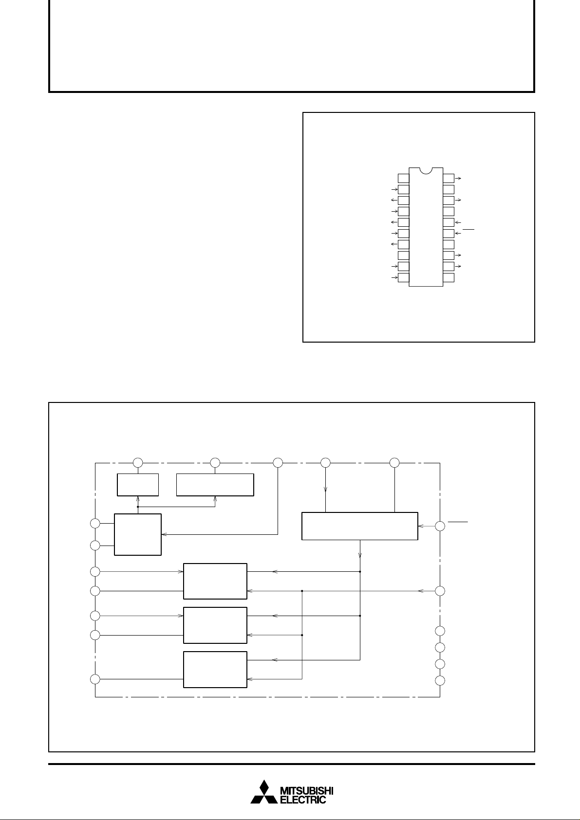
PIN CONFIGURATION (TOP VIEW)
1
1
V
CC1
2
CURRENT SETTING INPUT 1
CURRENT SETTING LOAD OUTPUT 1
CURRENT SETTING INPUT 2
CURRENT SETTING LOAD OUTPUT 2
CURRENT SETTING LOAD OUTPUT
LASER CURRENT
FORCED OFF INPUT
MONITORING LOAD INPUT 1
MONITORING LOAD INPUT 2
V
L1
1RC
V
L2
2RC
V
OFF
3RC
GND1
1RM
2RM
2
3
3
4
4
5
5
6
6
7
7
8
8
9
9
10
10
Outline
M66512P/FP
20P4
20P2N-A
M66512P/FP
20
19
18
17
16
15
14
13
12
11
LASER CURRENT
RO
LOAD OUTPUT
NC
LASER DIODE OUTPUT
LD
GND2
MONITORING DIODE INPUT
PD
DATA INPUT
DATA
V
CC2
MONITORING
CO
COMPARATOR OUTPUT
MONITORING ANALOG
MO
OUTPUT
NC
NC: No Connection
BLOCK DIAGRAM
MONITORING
Linear amp
9
1RM
2RM
V
1RC
V
2RC
3RC
L1
L2
Differential
10
2
3
4
5
7
OUTPUT
MO
OUTPUT
CO
PD LD RO
12 13 16 18
Comparator
(Vref=1.4V)
amp
Constant current
COMPARATOR
source(I
L1
)
Max.60mA
Constant current
source(I
L2
)
Max.30mA
Constant current
source(I
L3
)
Max.30mA
20
Current switching circuit
I
L=IL1+IL2+IL3
15
DATA
DATA INPUT
6
V
OFF
LASER CURRENT
FORCED OFF
1
CC1
V
14
V
CC2
GND
1
8
GND
17
2
V
L1
, 1RC : Laser current (IL1) setting pin
V
L2
, 2RC : Laser current (IL2) setting pin
3RC : Laser current (I
L3
) setting pin
V
CC1
, GND1 : Power supply pin for analog circuits in IC
V
CC2
, GND2 : Power supply pin for digital circuits in IC
1
Page 2
MITSUBISHI 〈DIGITAL ASSP〉
M66512P/FP
LASER-DIODE DRIVER
FUNCTION
The M66512 is a semiconductor laser-diode driver for driving
a specific type (Mitsubishi’s N type) of laser, in which the anode of a semiconductor laser diode is connected in stem
structure to the cathode of a monitoring photodiode.
The amplitude of laser drive current is set by applying a constant voltage from an external source. For that purpose, the
M66512 has two voltage applying pins, which they are independent each other, This mechanism makes it possible to set
a drive current with great accuracy.
PIN DESCRIPTIONS
Name
LD
PD
VL1
1RC
VL2
2RC
3RC
DATA
1RM,
2RM
MO
CO
VOFF
RO
VCC1
VCC2
GND1
GND2
Pin
Laser connection pin
Monitoring diode connection pin
Voltage input pin for IL1 setting
Load resistor connection pin for IL1 setting
Voltage input pin for IL2 setting
Load resistor connection pin for IL2 setting
Load resistor connection pin for IL3 setting
Switching data input pin
Load resistor connection pins for monitoring
function
Analog output pin for monitoring function
Comparator output pin for monitoring function
Laser current forced OFF input pin
Load resistor connection pin for laser current
Power supply pin 1
Power supply pin 2
GND pin 1
GND pin 2
As the IC is equipped with a pin to provide a forced OFF of
current circuit, it is possible to prevent a large current flowing
through laser diodes at the moment of power ON.
Regarding the detection of laser power, a monitor current
generated by a monitoring photodiode, which is incorporated
in laser unit, is drawn and converted into changes in voltage
by means of an external resistor, in order to output as an analog signal. Simultaneously, the converted voltage is compared with the internal reference voltage, thence the result is
output in TTL level as logic information.
Functions
Connect to cathode on semiconductor laser diode.
Connect to cathode on monitoring photodiode.
Voltage input to set output current (IL1) of current source 1.
Connect load resistor between this pin and GND for IL1 setting.
Voltage input to set output current (IL2) of current source 2.
Connect load resistor between this pin and GND for IL2 setting.
Connect load resistor between this pin and GND for IL3 setting.
Leave this pin open if IL3 is not used.
Laser turns on and off by “L” and “H”, respectively .
Connect resistor between pins 1RM and 2RM for conversion of
current generated by monitoring photodiode into changes in voltage.
Analog output for monitoring laser power
Comparator output for monitoring laser power
If this is “L”, all current supply circuits are turned off.
Connect load resistor between RO and VCC for laser current.
Power supply for internal analog circuits. Connect to positive power
source (+5V)
Power supply for internal digital circuits. Connect to positive power
source (+5V)
GND for internal analog circuits
GND for internal digital circuits
2
Page 3
MITSUBISHI 〈DIGITAL ASSP〉
M66512P/FP
LASER-DIODE DRIVER
OPERATION
1. Setting for Laser Drive Current
The M66512 has 3 built-in constant current sources, IL1, IL2,
L3. Each output current can be controlled independently .
and I
The following (1) to (3) describe the method for how to set
IL1,IL2, and IL3.
L1 setting method
(1)I
The value of I
L1 is determined by the voltage on the VL1
pin and the resistor (RC1) connected between the 1RC
pin and GND. The following equation is used for approximation.
L1[V]
L1 [mA] = 12 ×
I
V
RC1 [kΩ]
provided that 0≤VL1≤VCC–1.8V and IL1(max.) =60mA
(2)I
L2 setting method
The value of I
L2 is determined by the voltage on the VL2
pin and the resistor (RC2) connected between the 2RC
pin and GND. The following equation is used for approximation.
L2[V]
IL2[mA] = 6 ×
V
RC2 [kΩ]
provided that 0≤VL2≤VCC–1.8V and IL2(max.) =30mA
(3)I
L3 setting method
The value of I
voltage (V
L3 is determined by the internal reference
ref) and the resistor (RC3) connected between
the 3RC pin and GND. The following equation is used for
approximation.
ref[V]
IL3[mA] = 10 ×
V
RC3 [kΩ]
provided that Vref =1.4V (typ.) and IL3(max.) =30mA
Note: Each of the above equations is a typical on for ob-
taining I
L1–IL3. In practice values vary by a few per-
cent due to some reasons such as differences of
ICs from lot to lot and variations in operation temperatures.
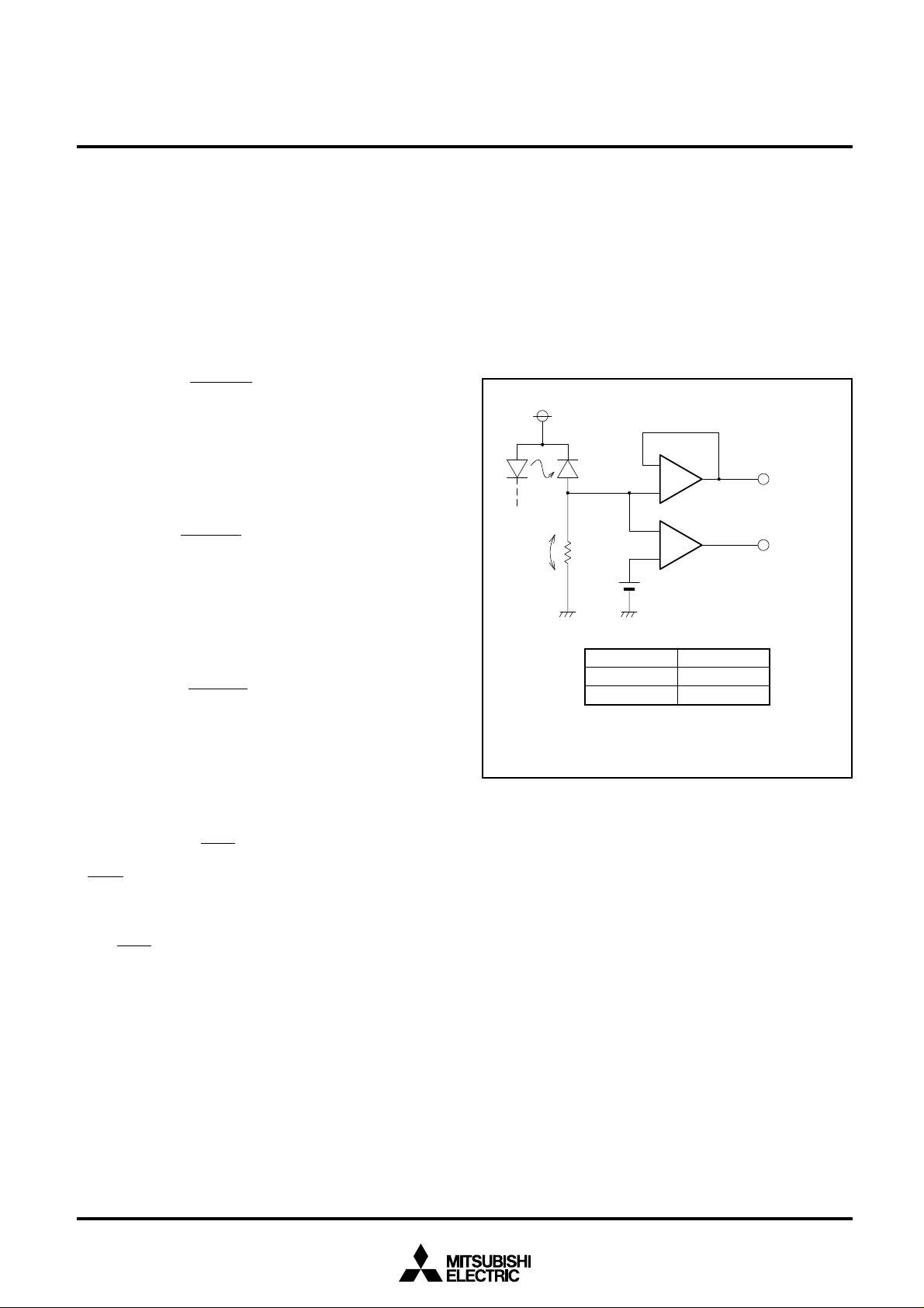
(1)A current equal to the PD current generated by laser light
flows through the resistor (RM) connected between 1RM
and 2RM. Then, a potential difference (V
M) proportional to
the output of laser light occurs at RM.
(2)The VM is output at the MO pin as an analog signal
through a buffer amp. At the same time, V
with the internal reference voltage V
M is compared
ref(1.4V typ.) by the
comparator, thence the result of the comparison is output
at the CO pin in TTL level.
LD
PD
RMVM
Vref
Condition CO output
VM<Vref “L”
VM>Vref “H”
_
+
+
_
Buffer amp
Comparator
MO output
CO output
A Schematic Diagram of Monitor Circuits
2. Switching Operation
The laser turns on if DA TA =“L”. The laser drive current at that
moment is I
L1 +IL2 + IL3.
If DATA = “H” the laser is turned off, and the laser drive current is almost zero irrespective of the values of I
L1 to IL3.
3. Use of the VOFF Input
When DA T A = “H” the current flowing through the laser is zero
so the laser is turned off, but the internal current sources are
in operation.
When V
OFF = “L” in contrast, the internal current sources are
turned off. Accordingly, it is possible to prevent an excessive
current from flowing through the laser by, for example, fixing
OFF input to “L” until VCC, after turned on, reaches
the V
3.5V(typ.). (See the section dealing with internal reset.)
4. Laser Power Monitoring Operation
At the MO and CO pins, the M66512 outputs data obtained
by the monitoring photodiode (PD) contained in the laser, in
the sequence explained below.
3
Page 4

MITSUBISHI 〈DIGITAL ASSP〉
M66512P/FP
LASER-DIODE DRIVER
5. RO Pin
The RO pin is used to connect a load resistor (RO) for the
current sources (I
nected between the RO pin and V
L1, IL2, and IL3). The load resistor is con-
CC in order to reduce the
power dissipated in the IC.
The resistance of the load resistor should be such that does
not generate a voltage equal to or lower than 2.5V at the RO
pin. Accordingly, a value that satisfies the following equation
should be chosen.
CC–2.5[V]
RO (Ω) ≤
maximum load current flowing through RO [A]
V
Example: If VCC =5V and the maximum load current is 120
mA, RO is 20Ω or under.
6. Internal Reset Function
The M66512 has a reset circuit for the protection of laser from
an excessive current flowing at the moment of power on. The
reset circuit functions in the range V
CC < 3.5V(typ.), letting all
current sources turn off.
CC and GND Pins
7. V
Pins related to the power supply function are V
CC1, VCC2,
GND1, and GND2. The role of these pins in terms of the internal circuits are as follows.
CC1, GND1 : connected to analog circuits
V
V
CC2, GND2 : connected to digital circuits
In practical wiring, the following should be noted.
(1) Secure as much a width as possible for conductors and
avoid lengthy wiring.
(2)Allocate electrolytic capacitors for stable voltage near
CC1 and GND1.
V
(3)Allocate by-pass capacitors near V
CC2 and GND2.
P=ICC × VCC +I(RO) × V(RO) + I(LD) × V(LD) + IOL(CO) × VOL(CO)
Where V(RO) : voltage at RO pin
(LD) : voltage at LD pin
V
(RO) : load current at RO pin
I
I
(LD) : load current at LD pin
OL(CO) : “L” output voltage at CO pin
V
OL(CO) : “L” output voltage at CO pin
I
If, for example, V
(LD) = 120mA, IOL(CO) = 8mA, and VOL(CO) = 0.5V , power dis-
I
CC = 5.25V, V(RO) = V(LD) = 2.75V, I(RO) =
sipation at times of turning on and off of laser will be as follows.
(1)Laser ON (DATA =“L” and I
P
ON = 75 × 5.25 + 0 + 120 × 2.75 + 8 × 0.5 = 727.8(mW)
(2)Laser OFF (DATA =“H” and I
OFF = 74 × 5.25 + 120 × 2.75 + 0 = 718.5(mW)
P
CC = 75mA)
CC = 74mA)
Notes on the Wiring for peripheral Components
Lay out peripheral components necessary for the M66512 to
operate in closest possible proximity to the M66512.
Calculation Method for Power Dissipation
The M66512’s approximated power dissipation, P, is determined by the following equation.
4
Page 5

OPERA TING WAVEFORMS
P0
MITSUBISHI 〈DIGITAL ASSP〉
M66512P/FP
LASER-DIODE DRIVER
Laser output
Laser output
IL3 IL1 IL2
Laser current IL
Drive current pulse
ABSOLUTE MAXIMUM RATINGS
Symbol
VCC
VI
VO
IL1
IL2
IL3
Pd
Tstg
Note 1: For operation above 25°C free-air temperature, derating of 10.4mW/°C is necessary.
2: For operation above 25°C free-air temperature, derating of 9.6mW/°C is necessary.
Supply voltage
Input voltage
Output voltage
Output current 1
Output current 2
Output current 3
Power dissipation
Storage temperature
Parameter
VL1, VL2
DAT A, VOFF
CO
RO
DIP
SOP
Output: “H”
For single integrated circuit; Ta=25˚C (Note 1)
IC Measured being mounted; Ta=25˚C (Note 2)
Conditions
IL1 : 0~60mA
IL2 : 0~30mA
IL3 : 0~30mA
Ratings
–0.5 ~ +7.0
–0.3 ~ VCC
–0.3 ~ + 7
–0.3 ~ + 5.5
–0.3 ~ + 7
90
45
45
1300
1200
–65 ~ 150
Unit
V
V
V
mA
mA
mA
mW
°C
RECOMMENDED OPERATIONAL CONDITIONS
VCC
IL1
IL2
IL3
Topr
Symbol
Supply voltage
Output current 1
Output current 2
Output current 3
Operational ambient temperature
Parameter
Conditions
Min.
4.75
–20
Limits
Typ.
5
Max.
5.25
60
30
30
75
Unit
V
mA
mA
mA
˚C
5
Page 6

MITSUBISHI 〈DIGITAL ASSP〉
M66512P/FP
LASER-DIODE DRIVER
ELECTRICAL CHARACTERISTICS (VCC = 5V ± 5%, Ta = –20 ~ 75˚C unless otherwise noted))
Symbol
VIH
VIL
VI
VOH
VOL
VLD
VOS
∆VM
II
Vref
IL1
IL2
IL3
IOFF
ICC
Note 3. IMO: Output current at MO pin. IPD: Input current at PD pin
4. RM: Resistor connected between 1RM and 2RM pins
5. These parameters indicate the conversion characteristics of the input voltage and output current. In actual use, IL1 – IL3 shall be within the range
specified as limits in the recommended operating conditions.
* Typical values are gained under conditions of V
values are gained under the condition V
“H” input voltage
“L” input voltage
Maximum effective input voltage
“H” output voltage
“L” output voltage
Operating voltage range
Output offset voltage
Output voltage
fluctuation
Input current
Reference voltage
Output current 1 (Note 5)
Output current 2 (Note 5)
Output current 3 (Note 5)
OFF state output current
Supply current
Parameter
CC = 5V.
Test conditions
DAT A, VOFF
Min.
2
DAT A, VOFF
VL1, VL2
CO
CO
IOH=–400µA
IOL=4mA
IOL=8mA
LD
MO
MO
Temperature coefficient
DAT A, VOFF
VL1, VL2
Temperature coefficient
LD
Temperature coefficient
LD
Temperature coefficient
LD
LD
IMO=±20µA, IPD=0mA (Note 3)
IPD=0.2~2.0mA, IMO=±20µA
RM=1kΩ (Note 4)
RM=1kΩ, IPD=1.2mA
VI=2.7V
VI=0.4V
VI=0~VCC
Ta=–20~25˚C
Ta=25~75˚C
VL1=3V , RC1=560 Ω, VLD=2V
VL2=3V , RC2=560 Ω, VLD=2V
RC3=360Ω, VLD=2V
VOFF=DATA=2V
VOFF=DATA=0.8V
VCC=5.25V , V
OFF
=4.5V ,
VL1=VL2=3.0V ,
RC1=RC2=560Ω,
RC3=360Ω,
RO=LD=5.0V
CC =5V and Ta =25˚C. Regarding parameters that Ta is specified as test condition, however, typical
VCC–1.8
2.7
VCC–2.5
DATA
=0V
DATA
=4.5V
Limits
Typ.*
VCC–1.4
30
20
0.05
1.4
–0.8
–0.5
61
0.111
31
0.050
34
0.03
0.01
60
59
Max.
0.8
0.4
0.5
VCC
20
–0.2
±1
50
50
75
74
Unit
V
V
V
V
V
V
mV
mV
mV/˚C
µA
mA
µA
V
mV/˚C
mA
mA/˚C
mA
mA/˚C
mA
µA
µA
mA
SWITCHING CHARACTERISTICS (VCC = 5V, Ta = –25˚C)
Input
VL1, VL2
Voltage
PD
Current
PD
Current
V
OFF
Voltage
V
OFF
Voltage
Test pin
LD
Current
MO
Voltage
CO
Voltage
LD Current
LD Current
6
fOP
tRP1
tRP2
tRP3
tON
tOFF
Symbol
Parameter
Operating frequency
Circuit response time 1
Circuit response time 2
Circuit response time 3
Circuit ON time
Circuit OFF time
Output
Test conditions
ILD(L)=0mA, ILD(H)=60mA (Note 6)
I
LD(L)
=55mA, I
LD(H)
=65mA(Note 6)
IPD(L)=0mA, IPD(H)=2mA,
RM=1kΩ (Note 7)
|∆IPD|=0.2mA, RM=1kΩ (Note 7)
|∆IPD|=1mA (Note 7)
|∆IPD|=0.2mA (Note 7)
ILD(H)=60mA, ILD(L)=0mA (Note 8)
ILD(H)=60mA, ILD(L)=0mA (Note 8)
Min.
Limits
Typ.
40
4.5
0.5
7
1
7
0.5
3
0.5
Max.
7
2
10
3
10
2
5
2
Unit
Mbps
µs
µs
µs
µs
µs
Page 7

MITSUBISHI 〈DIGITAL ASSP〉
NOTE 6: MEASURING CIRCUIT NOTE 7: MEASURING CIRCUIT
M66512P/FP
LASER-DIODE DRIVER
5V
VCC
RO
PD
LD
DATA
20Ω
LD
I
Oscilloscope
(output)
Current probe
560Ω
560Ω
Oscilloscope
P.G.
r=tf=6ns
t
(input)
50Ω
560Ω
560Ω
VL1
VL2
1RC
2RC
1RM
RM
2RM
GND
Other pins are opend
TIMING CHART TIMING CHART
V
VL1, V
I
LD
L2
50% 50%
t
RP1
t
RP1
90%
10%
IH
V
IL
I
LD(H)
I
LD(L)
PD
I
MO,CO
(✽): I
20Ω
5V
V
V
L1
V
L2
1RC
2RC
1RM
2RM
CC
RO
DATA
PD
CO
MO
Oscilloscope
(input)
PD
I
Oscilloscope
(output)
Current probe
50Ω
t
r=tf
P.G.
=6ns
GND
Other pins are opend
I
| I
PD
50% 50%
t
RP2,
t
RP3
MO=10%
CO=1.5V
PD
gained at the moment CO output is inverted.
t
RP2,
t
RP3
MO=90%
CO=1.5V
| I
PD
|
I
|
I
V
V
PD(H)
PD(T)( ✽ )
PD(L)
OH
OL
NOTE 8: MEASURING CIRCUIT TIMING CHART
5V
Oscilloscope
Current probe
I
LD
(output)
V
OFF
I
LD
Oscilloscope
(input)
P.G.
r=tf
=6ns
t
50Ω
560Ω
560Ω
V
L1
V
L2
1RC
2RC
1RM
2RM
V
OFF
V
CC
DATA
GND
20Ω
RO
PD
LD
Other pins are opend
1.5V
t
OFF
10%
1.5V
t
ON
90%
3V
0V
LD(H)
I
I
LD(L)
7
Page 8

APPLICATION EXAMPLE
M66512
1RM
2RM
1RC
2RC
3RC
9
10
2
L1
V
3
4
V
L2
5
7
RM
RC1
RC2
RC3
Controller
RO
MO CO PD LD RO
Linear
amp.
Differential
amp.
Comparator
(Vref=1.4V)
Consttant current
source(IL1)
Max.60mA
Consttant current
source(I
L2
Max.30mA
Consttant current
source(I
Max.30mA
)
L3
)
Current switching circuit DATA STREAM
2018161312
IL=IL1+IL2+I
MITSUBISHI 〈DIGITAL ASSP〉
M66512P/FP
LASER-DIODE DRIVER
15
DATA
L3
DATA INPUT
6
V
OFF
CONTROL SIGNAL
LASER CURRENT FORCED OFF
1
V
CC1
14
V
CC2
8
GND1
GND2
17
8
Page 9

TYPICAL CHARACTERISTICS (VCC=5V, Ta=25˚C)
MITSUBISHI 〈DIGITAL ASSP〉
M66512P/FP
LASER-DIODE DRIVER
LASER CURRENT VS. CURRENT SETTING VOLTAGE
100
IL1 +IL2
80
60
40
20
LASER CURRENT IL1, IL2 (mA)
0
012345
CURRENT SETTING INPUT VOLTAGES V
MO OUTPUT VS. MONITORING CURRENT
(V)
5
MO
IL1(RC1=560Ω)
L2(RC2=560Ω)
I
L1, VL2 (V)
LASER CURRENT VS. RC3 RESISTANCE
50
40
(mA)
L3
30
20
LASER CURRENT I
10
0
0.2 0.4 0.6 0.8 1.0 1.2
RC3 RESISTANCE (kΩ)
CO OUTPUT VS. MONITORING CURRENT
(V)
CO
5
4
3
2
1
MONITORING ANALOG OUTPUT V
0
012345
MONITORING CURRENT I
V
RM=1kΩ
PD
(mA)
MO
4
3
2
RM=1kΩ
1
0
1.0 1.2 1.4 1.6 1.8 2.0
MONITORING COMPARATOR OUTPUT V
MONITORING CURRENT IPD (mA)
9
Page 10

EVALUATION OF SWITCHING OPERATION WAVEFORMS
V
Connector
CC
V
GND
L1
V
VL2
VOFF
GND
CO
MO
DATA
PD
10
1
2
3
4
5
6
7
8
9
0.1µF
CC=5V
Ta=25°
22µF
JP
RM
3kΩ
C
680Ω
680Ω
680Ω
RC1
RC2
RC3
10
1
2
3
4
5
6
7
8
9
VCC1
VL1
1RC
VL2
2RC
OFF
V
3RC
GND1
1RM
2RM
1RO
NC
LD
GND2
PD
DATA
CC2
V
CO
MO
NC
20
19
18
17
16
15
14
13
12
11
RO
20Ω
0.1
µF
MITSUBISHI 〈DIGITAL ASSP〉
LASER-DIODE DRIVER
ML44114N
100Ω
(
)
✽
R
LD
()
✽
300pF
C
LD
( ): Optimum values of R
✽
may vary depending on the kind
of the laser in use and the pattern
of the printed board.
RD
2Ω
M66512P/FP
Light intensity
meter
50Ω
Oscilloscope
(laser light output)
LD and CLD
Oscilloscope (data input)
P.G.
(Note 9)
50Ω
Note 9. tr=tf=6ns, VO=3VP-P, duty=50%
SWITCHING OPERATION WAVEFORMS
3V
DATA input
(2V/div)
0V
3mW
Laser light output
(1mW/div)
0mW
Evaluation Circuit
10Mbit/s (t : 50ns/div) 20Mbit/s (t : 20ns/div)
25Mbit/s (t : 20ns/div) 40Mbit/s (t : 10ns/div)
10
Note: The delay from the DATA input to the laser light output contains the delay occurring in measuring systems.
 Loading...