

Page 1
MITSUBISHI 〈DIGITAL ASSP〉
MITSUBISHI 〈DIGITAL ASSP〉
DESCRIPTION
The M66256FP is a high-speed line memory with a FIFO
(First In First Out) structure of 5120-word × 8-bit configuration
which uses high-performance silicon gate CMOS process
technology.
It has separate clock, enable and reset signals for write and
read, and is most suitable as a buffer memory between devices with different data processing throughput.
FEATURES
• Memory configuration ........................................................
............................. 5120 words × 8-bits (dynamic memory)
• High-speed cycle ............................................. 25ns (Min.)
• High-speed access ......................................... 18ns (Max.)
• Output hold ........................................................ 3ns (Min.)
• Fully independent, asynchronous write and read operations
• Variable length delay bit
• Output ....................................................................3 states
APPLICATION
Digital photocopiers, high-speed facsimile, laser beam printers.
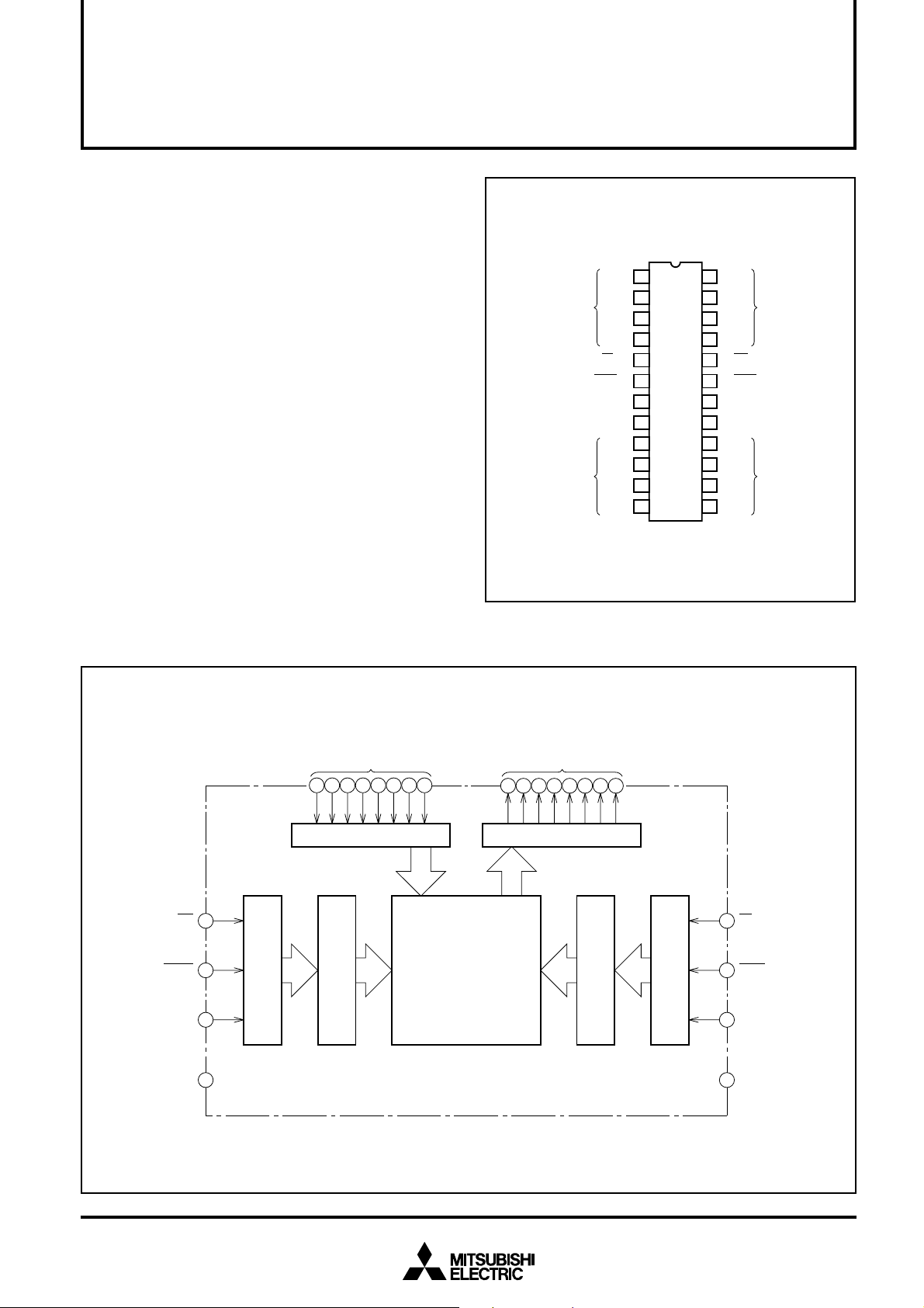
M66256FP
5120 × 8-BIT LINE MEMORY (FIFO)
5120 × 8-BIT LINE MEMORY (FIFO)
PIN CONFIGURATION (TOP VIEW)
←
0
Q
Q
Q
Q
READ ENABLE INPUT
READ RESET INPUT
READ CLOCK INPUT
DATA OUTPUT
RE
RRES
GND
RCK
Q
Q
Q
Q
1
←
1
2
←
2
3
←
3
4
→
5
→
6
7
→
8
←
4
9
←
5
10
←
6
11
←
7
12
Outline 24P2U-A
24
23
22
21
M66256FP
20
19
18
17
16
15
14
13
M66256FP
←
D
0
←
D
1
DATA INPUTDATA OUTPUT
←
D
2
←
D
3
←
WRITE ENABLE INPUT
WE
←
WRITE RESET INPUT
WRES
CC
V
←
WCK
WRITE CLOCK INPUT
←
D
4
←
D
5
DATA INPUT
←
6
D
←
D
7
BLOCK DIAGRAM
WRITE
ENABLE INPUT
WRITE
RESET INPUT
WRITE
CLOCK INPUT
WE
WRES
WCK
CC
V
DATA INPUT
~~
0D7
D
13
14 15 16 21 22 23 24
INPUT BUFFER
20
MEMORY ARRAY OF
19
17
WRITE CONTROL CIRCUIT
18
WRITE ADDRESS COUNTER
5120-WORD × 8-BIT
CONFIGURATION
DATA OUTPUT
Q
0Q7
1 2 3 4 9 10 11 12
OUTPUT BUFFER
READ ADDRESS COUNTER
5
6
8
READ CONTROL CIRCUIT
7
ENABLE INPUT
READ
RRES
RESET INPUT
READ
RCK
CLOCK INPUT
GND
READ
RE
1
Page 2
MITSUBISHI 〈DIGITAL ASSP〉
M66256FP
5120 × 8-BIT LINE MEMORY (FIFO)
FUNCTION
When write enable input WE is “L”, the contents of data inputs
D0 to D7 are written into memory in synchronization with rise
edge of write clock input WCK. At this time, the write address
counter is also incremented simultaneously .
The write function given below are also performed in synchronization with rise edge of WCK.
When WE is “H”, a write operation to memory is inhibited and
the write address counter is stopped.
When write reset input WRES is “L”, the write address counter
is initialized.
When read enable input RE is “L”, the contents of memory are
output to data outputs Q
edge of read clock input RCK. At this time, the read address
counter is also incremented simultaneously .
The read functions given below are also performed in synchronization with rise edge of RCK.
When RE is “H”, a read operation from memory is inhibited
and the read address counter is stopped. The outputs are in
the high impedance state.
When read reset input RRES is “L”, the read address counter
is initialized.
ABSOLUTE MAXIMUM RATINGS (Ta = 0 ~ 70°C, unless otherwise noted)
VCC
VI
VO
Pd
Tstg
Symbol
Supply voltage
Input voltage
Output voltage
Maximum power dissipation
Storage temperature
Parameter
A value based on GND pin
Ta = 25°C
RECOMMENDED OPERATING CONDITIONS
Parameter
Min.
4.5
0
VCC
GND
Topr
Symbol
Supply voltage
Supply voltage
Operating ambient temperature
Conditions
Limits
Typ.
5
0
0 to Q7 in synchronization with rise
Ratings
–0.5 ~ +7.0
–0.5 ~ VCC + 0.5
–0.5 ~ VCC + 0.5
440
–65 ~ 150
Max.
5.5
70
Unit
V
V
°C
Unit
V
V
V
mW
°C
ELECTRICAL CHARACTERISTICS (Ta = 0 ~ 70°C, VCC = 5V ± 10%, GND = 0V)
Parameter
Test conditions
IOH = –4mA
IOL = 4mA
WE, WRES, WCK, RE,
VI = VCC
VI = GND
VO = VCC
VO = GND
VI = VCC, GND, Output open
tWCK, tRCK = 25ns
f = 1MHz
f = 1MHz
RRES, RCK,
D0 ~ D7
WE, WRES, WCK, RE,
RRES, RCK,
D0 ~ D7
VIH
VIL
VOH
VOL
IIH
IIL
IOZH
IOZL
ICC
CI
CO
Symbol
“H” input voltage
“L” input voltage
“H” output voltage
“L” output voltage
“H” input current
“L” input current
Off state “H” output current
Off state “L” output current
Operating mean current dissipa-
tion
Input capacitance
Off state output capacitance
2.0
VCC–0.8
Limits
Typ.Min.
Max.
0.8
0.55
1.0
–1.0
5.0
–5.0
80
10
15
Unit
V
V
V
V
mA
mA
mA
mA
mA
pF
pF
2
Page 3
SWITCHING CHARACTERISTICS (Ta = 0 ~ 70°C, VCC = 5V ± 10%, GND = 0V)
Parameter
tAC
tOH
tOEN
tODIS
Symbol
Access time
Output hold time
Output enable time
Output disable time
TIMING CONDITIONS (Ta = 0 ~ 70°C, VCC = 5V ± 10%, GND = 0V, unless otherwise noted)
Symbol
tWCK
tWCKH
tWCKL
tRCK
tRCKH
tRCKL
tDS
tDH
tRESS
tRESH
tNRESS
tNRESH
tWES
tWEH
tNWES
tNWEH
tRES
tREH
tNRES
tNREH
tr, tf
tH
Notes 1: For 1-line access, the following should be satisfied:
WE “H” level period ≤ 20ms – 5120 t
RE “H” level period ≤ 20ms – 5120 t
2: Perform reset operation after turning on power supply.
Write clock (WCK) cycle
Write clock (WCK) “H” pulse width
Write clock (WCK) “L” pulse width
Read clock (RCK) cycle
Read clock (RCK) “H” pulse width
Read clock (RCK) “L” pulse width
Input data setup time to WCK
Input data hold time to WCK
Reset setup time to WCK or RCK
Reset hold time to WCK or RCK
Reset nonselect setup time to WCK or RCK
Reset nonselect hold time to WCK or RCK
WE setup time to WCK
WE hold time to WCK
WE nonselect setup time to WCK
WE nonselect hold time to WCK
RE setup time to RCK
RE hold time to RCK
RE nonselect setup time to RCK
RE nonselect hold time to RCK
Input pulse rise/fall time
Data hold time (Note 1)
WCK – WRES “L” level period
RCK – RRES “L” level period
Parameter
MITSUBISHI 〈DIGITAL ASSP〉
M66256FP
5120 × 8-BIT LINE MEMORY (FIFO)
25
11
11
25
11
11
Limits
Typ.Min.
3
3
3
Limits
Typ.Min.
7
3
7
3
7
3
7
3
7
3
7
3
7
3
Max.
18
18
18
Max.
20
20
Unit
ns
ns
ns
ns
Unit
ns
ns
ns
ns
ns
ns
ns
ns
ns
ns
ns
ns
ns
ns
ns
ns
ns
ns
ns
ns
ns
ms
3
Page 4
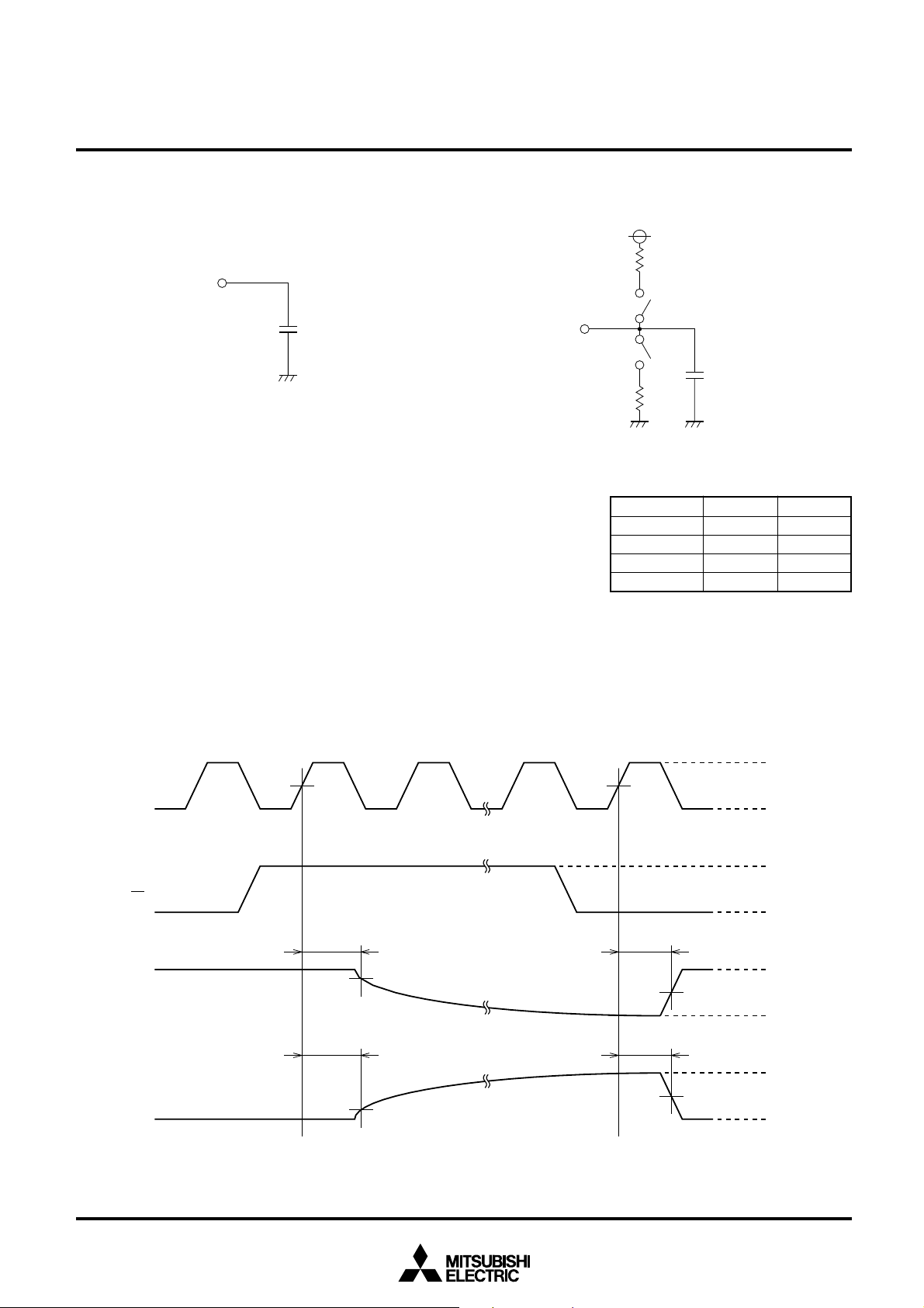
TEST CIRCUIT
MITSUBISHI 〈DIGITAL ASSP〉
M66256FP
5120 × 8-BIT LINE MEMORY (FIFO)
V
CC
RL=1kΩ
Q
n
SW1
Q
CL=30pF : tAC, t
OH
n
SW2
R
L
=1kΩ
CL=5pF : t
OEN
, t
ODIS
Input pulse level : 0 ~ 3V
Input pulse rise/fall time : 3ns
Decision voltage input : 1.3V
Decision voltage output : 1.3V (However, t
The load capacitance C
probe.
that for decision).
L includes the floating capacitance of connection and the input capacitance of
tODIS/tOEN TEST CONDITION
RCK
RE
ODIS(LZ) is 10% of output amplitude and tODIS(HZ) is 90% of
1.3V
ODIS(HZ)
t
Parameter
tODIS(LZ)
tODIS(HZ)
tOEN(ZL)
tOEN(ZH)
1.3V
t
OEN(ZH)
SW1
Closed
Open
Closed
Open
SW2
Open
Closed
Open
Closed
3V
GND
3V
GND
V
n
Q
t
ODIS(LZ)
Q
n
90%
10%
t
OEN(ZL)
1.3V
1.3V
OH
V
OL
4
Page 5

OPERATING TIMING
• Write cycle
WCK
MITSUBISHI 〈DIGITAL ASSP〉
M66256FP
5120 × 8-BIT LINE MEMORY (FIFO)
Cycle n Cycle n+1 Cycle n+2 Disable cycle Cycle n+3 Cycle n+4
WE
n
D
• Write reset cycle
t
WCK
tDSt
t
WCKHtWCKL
DH
t
WEHtNWES
t
t
NWEH
WES
t
DS
DH
t
(n+2) (n+3)( n+1)(n) (n+4)
WRES = “H”
WCK
WRES
n
D
Cycle n–1 Cycle n Reset cycle Cycle 2Cycle 0 Cycle 1
t
WCK
t
NRESHtRESS
tDHt
DS
t
RESHtNRESS
tDHt
DS
(n–1) (n) (0) (1) (2)
WE = “L”
5
Page 6

• Matters that needs attention when WCK stops
n cycle n+1 cycle n cycle Disable cycle
WCK
tWCK
WE
tDS tDH tDS tDH
t
NWES
MITSUBISHI 〈DIGITAL ASSP〉
M66256FP
5120 × 8-BIT LINE MEMORY (FIFO)
n
D
(n)
Period for writing data (n)
into memory
(n)
Period for writing data (n)
into memory
WRES = “H”
Input data of n cycle is read at the rising edge after WCK of n cycle and writing operation starts in the WCK low-level period of
n+1 cycle. The writing operation is complete at the falling edge after n+1 cycle.
To stop reading write data at n cycle, enter WCK before the rising edge after n+1 cycle.
When the cycle next to n cycle is a disable cycle, WCK for a cycle requires to be entered after the disable cycle as well.
6
Page 7

• Read cycle
RCK
RE
Cycle n Disable cycle Cycle n+3 Cycle n+4Cycle n+2Cycle n+1
tRCK tRCKH tRCKL tREH tNRES tNREH tRES
MITSUBISHI 〈DIGITAL ASSP〉
M66256FP
5120 × 8-BIT LINE MEMORY (FIFO)
t
AC
Q
n
• Read reset cycle
RCK
tODIS
(n) (n+1) (n+2) (n+3) (n+4)
Cycle n–1 Cycle 0 Cycle 2Cycle n Reset cycle Cycle 1
t
RCK
t
NRESHtRESS
HIGH-Z
t
RESHtNRESS
tOEN
tOH
RRES = “H”
RRES
Q
n
t
AC
(n–1) (n) (0) (0) (0) (1) (2)
t
OH
RE = “L”
7
Page 8

MITSUBISHI 〈DIGITAL ASSP〉
M66256FP
5120 × 8-BIT LINE MEMORY (FIFO)
VARIABLE LENGTH DELAY BITS
• 1-line (5120 bits) delay
A write input data is written into memory at the second rise edge of WCK in the cycle, and a read output data is output from
memory at the first rise edge of RCK in the cycle, so that 1-line delay can be made easily.
Cycle 0 Cycle 1 Cycle 2 Cycle 5118 Cycle 5119
WCK
RCK
t
RESStRESH
WRES
RRES
tDSt
DH
D
n
Q
n
(0)
(1) (2)
5120 cycles
• N-bit delay bit
(Making a reset at a cycle corresponding to delay length)
Cycle 5120
(5117) (5118) (5119)
Cycle 5121
(0')
t
DS
DH
t
(0') (1') (2') (3')
t
t
AC
OH
(0) (1) (2) (3)
(1')
Cycle 5122
(2')
WE, RE = “L”
WCK
RCK
WRES
RRES
D
n
Q
n
Cycle 0 Cycle 1 Cycle 2 Cycle n–2 Cycle n–1
t
RESStRESH
tDSt
DH
(0)
(1) (2) (n–3) (n–2) (n–1) (0') (1') (2') (3')
m cycles
Cycle n
t
RESStRESH
t
Cycle n+1
(0')
t
DS
DH
t
t
AC
OH
(0) (1) (2) (3)
(1')
Cycle n+2
(2')
Cycle n+3
(3')
WE, RE = “L”
3
m ≥
8
Page 9

MITSUBISHI 〈DIGITAL ASSP〉
M66256FP
5120 × 8-BIT LINE MEMORY (FIFO)
• N-bit delay 2
_____
_____
(Sliding WRES and RRES at a cycle corresponding to delay length)
Cycle 0 Cycle 1 Cycle 2 Cycle n–2 Cycle n–1 Cycle n Cycle n+1 Cycle n+2 Cycle n+3
WCK
RCK
t
RESS
t
RESH
WRES
t
RESStRESH
RRES
tDSt
DH
n
D
Q
n
(0) (1) (2) (n–2) (n–1) (n) (n+1) (n+2) (n+3)
m cycles
tDSt
DH
AC
t
t
OH
(0) (1) (2) (3)
• N-bit delay 3
__
(Disabling RE at a cycle corresponding to delay length)
Cycle 0 Cycle 1 Cycle 2 Cycle n–1 Cycle n Cycle n+1 Cycle n+2 Cycle n+3
WCK
RCK
tRESS tRESH
WRES
RRES
RE
n
D
(0) (1) (2) (n–2) (n–1) (n) (n+1) (n+2) (n+3)
m cycles
NREH tRES
t
tDS tDHtDS tDH
t
AC tOH
WE, RE = "L"
m ≥
3
Qn
HIGH-Z
(0) (1) (2) (3)
WE = “L”
m ≥ 3
9
Page 10

MITSUBISHI 〈DIGITAL ASSP〉
M66256FP
5120 × 8-BIT LINE MEMORY (FIFO)
• Shortest read of data “n” written in cycle n
Cycle n–1 on read side should be started after end of cycle n+1 on write side
When the start of cycle n–1 on read side is earlier than the end of cycle n+1 on write side, output Qn of cycle n becomes invalid.
In the figure shown below, the read of cycle n–1 is invalid.
Cycle n Cycle n+1 Cycle n+2 Cycle n+3
WCK
D
n
RCK
Q
n
Cycle n–2 Cycle n–1 Cycle n
invalid (n)
(n+3)(n) (n+2)(n+1)
• Longest read of data “n” written in cycle n: 1-line delay
Cycle n <1>* on read side should be started when cycle n <2>* on write is started
Output Qn of n cycle <1>* can be read until the start of reading side n cycle <1>* and the start of writing side n cycle <2>* overlap each other.
Cycle n <1>* Cycle 0 <2>* Cycle n <2>*
WCK
10
D
n
RCK
n
Q
(n–1)<0>*
(n–1)<2>* (n)<2>*(n–1)<1>* (00) <2>*(n)<1>*
Cycle n <0>* Cycle 0 <1>* Cycle n <1>*
(n)<0>*
(0)<1>* (n–1)<1>* (n)<1>*
<0>*, <1>* and <2>* indicates a line value.
Page 11

APPLICATION EXAMPLE
Laplacian Filter Circuit for Correction of Resolution in the Secondary Scanning Direction.
MITSUBISHI 〈DIGITAL ASSP〉
M66256FP
5120 × 8-BIT LINE MEMORY (FIFO)
B
Line (n+1)
image data
M66256
D
0
~
D
9
1-line
delay
M66256
D
0
~
D
9
1-line
delay
Q
~
Q
Q
~
Q
0
9
0
9
A
Line (n–1)
image data
×2
Adder
A+B
N
Line n image data
2N–(A+B)
Subtractor
×K
{2N–(A+B)}
Adder
N+K
Corrected
image data
Primary scanning
direction
Secondary scanning
direction
A
N
B
Line (n–1)
Line n
Line (n+1)
N' = N+K {
(N–A)+(N–B)}
= N+K {
2N–(A+B)}
K : Laplacean coefficient
11
 Loading...