

Page 1
MITSUBISHI 〈DIGITAL ASSP〉
MITSUBISHI 〈DIGITAL ASSP〉
DESCRIPTION
The M66220 is a mail box that incorporates a complete CMOS shared
memory cell of 256 × 8-bit configuration using high-performance silicon
gate CMOS process technology, and is equipped with two access
ports of A and B.
Access ports A and B are equipped with independent addresses CS,
WE and OE control pins and I/O pins to allow independent and
asynchronous read/write operations from/to shared memory
individually. This product also incorporates a port adjustment
arbitration function in address contention from both ports.
FEATURES
• Memory configuration of 256 × 8 bits
• High-speed access, address access time 40ns (typ.)
• Complete asynchronous accessibility from ports A and B
• Completely static operation
• Built-in port arbitration function
• Low power dissipation CMOS design
• 5V single power supply
• Not Ready output pin is provided (open drain output)
• TTL direct-coupled I/O
• 3-state output for I/O pins
APPLICATION
Inter-MPU data transfer memory, buffer memory for image processing
system.
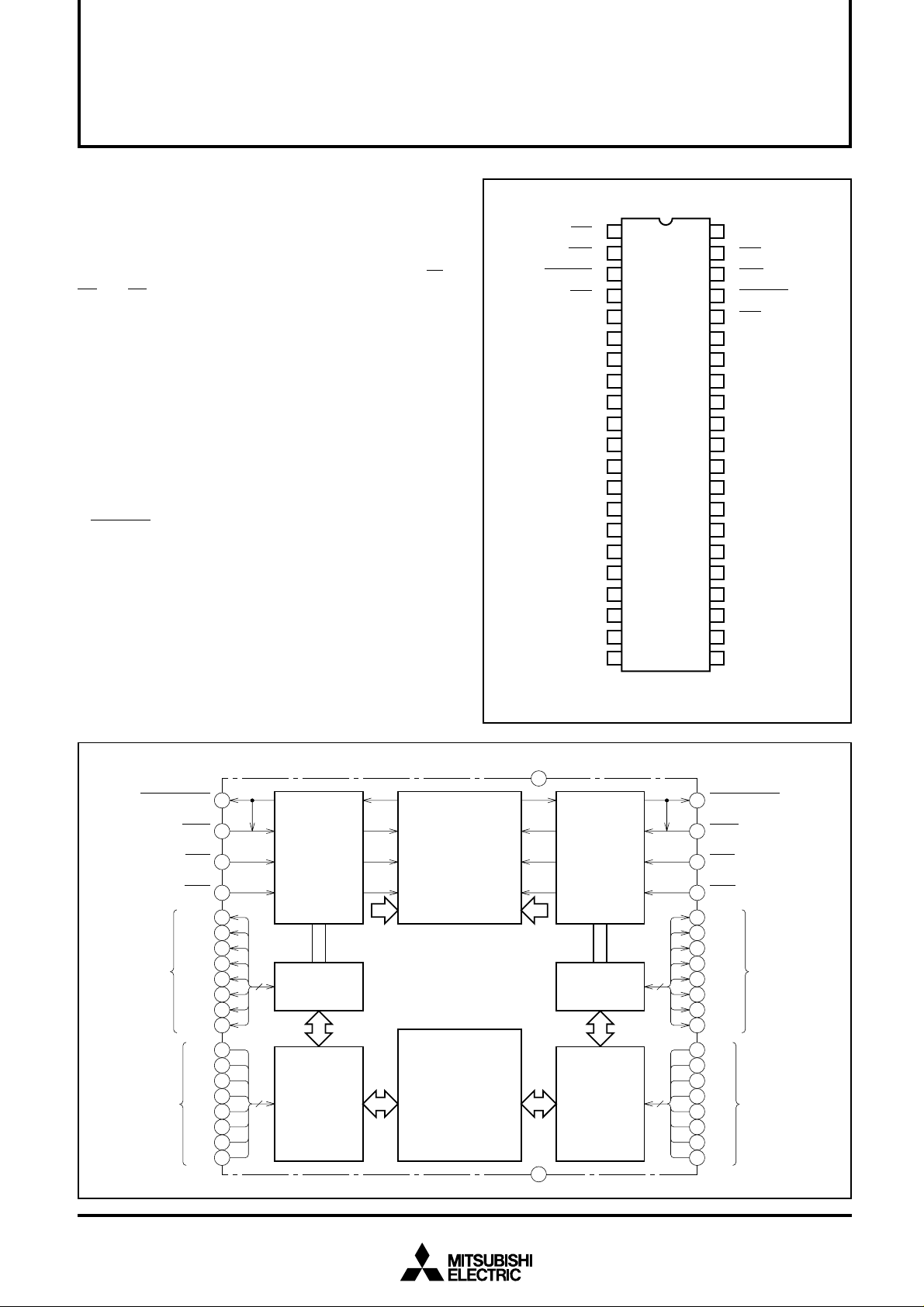
M66220SP/FP
M66220SP/FP
256 × 8-BIT MAIL-BOX
256 × 8-BIT MAIL-BOX
PIN CONFIGURATION (Top view)
CHIP SELECT
INPUT
WRITE ENABLE
INPUT
NOT READY
OUTPUT
OUTPUT ENABLE
INPUT
A PORT
ADDRESS
INPUT
A PORT
DATA I/O
Not Ready A
CSA
WEA
OEA
A
A
A
A
A
A
A
A
I/O
I/O
I/O
I/O
I/O
I/O
I/O
I/O
GND
→
1
→
2
←
3
→
4
→
5
0
A
→
6
1
A
→
7
2
A
→
8
3
A
→
9
4
A
→
10
5
A
→
11
6
A
→
12
7
A
↔
0
A
13
↔
14
1
A
↔
15
2
A
↔
16
3
A
↔
17
4
A
↔
18
5
A
↔
19
6
A
↔
20
7
A
21
M66220SP/FP
42
←
41
←
40
→
39
←
38
←
37
←
36
←
35
←
34
←
33
←
32
←
31
←
30
↔
29
↔
28
↔
27
↔
26
↔
25
↔
24
↔
23
↔
22
V
CSB
WEB
Not Ready B
OEB
A
A
A
A
A
A
A
A
I/O
I/O
I/O
I/O
I/O
I/O
I/O
I/O
CC
CHIP SELECT
INPUT
WRITE ENABLE
INPUT
NOT READY
OUTPUT
OUTPUT ENABLE
INPUT
0
B
1
B
2
B
B PORT
3
B
ADDRESS
INPUT
4
B
5
B
6
B
7
B
7
B
6
B
5
B
4
B
B PORT
DATA I/O
3
B
2
B
1
B
0
B
BLOCK DIAGRAM
NOT READY
OUTPUT
Not Ready A
WRITE
ENABLE INPUT
CHIP
SELECT INPUT
OUTPUT
ENABLE INPUT
A PORT DATA I/O
A PORT
ADDRESS INPUT
WEA
CSA
OEA
I/O0A
I/O
1
I/O
2
I/O
3
I/O
4
I/O
5
6
I/O
7
A0A
1
A
2
A
3
A
A
4
5
A
6
A
7
3
2
1
4
13
14
A
15
A
16
A
17
A
18
A
19I/O
A
20
A
5
6
A
7
A
8
A
9
A
10
A
11
A
12A
A
CONTROL
CIRCUIT
OEA
8
I/O BUFFER
8
ROW/COLUMN
DECODER
WEA
ARBITRATION
CIRCUIT
A
0
A
~
A
7
A
MEMORY ARRAY OF
256-WORD × 8-BIT
CONFIGURATION
CC
V
42
A
0
B
WEB
~
A
7
B
I/O BUFFER
ROW/COLUMN
21
GND
Outline
CONTROL
CIRCUIT
OEB
DECODER
42P4B
42P2R-A
39
40
41
38
22
23
24
25
8
26
27
28
29
37
36
35
8
34
33
32
31
30
Not Ready B
WRITE
WEB
ENABLE INPUT
CHIP
CSB
SELECT INPUT
OUTPUT
OEB
ENABLE INPUT
I/O0B
I/O
1
B
I/O
2
B
I/O
3
B
B PORT DATA I/O
I/O
4
B
I/O
5
B
I/O
6
B
I/O
7
B
A0B
1
B
A
2
B
A
B PORT
3
B
A
ADDRESS INPUT
A
4
B
5
B
A
6
B
A
7
B
A
NOT READY
OUTPUT
1
Page 2
MITSUBISHI 〈DIGITAL ASSP〉
M66220SP/FP
256 × 8-BIT MAIL-BOX
FUNCTION
The M66220 is a mail box most suitable for inter-MPU data transfer
which is used in a multiport mode. Provision of two pairs of addresses
and data buses in its shared memory cell of 256 × 8 bit configuration
allows independent and asynchronous read/write operations from/to
two access ports of A and B individually.
This allows access to shared memory as simple RAM when viewing
from one MPU. The concurrent accessibility to shared memory from
two MPUs provides remarkable improvement of a multiport mode
processor system in throughput.
The arbitration function incorporated in the chip decides the first-in
port to assign a higher priority to the access from one MPU, even if
two MPUs contend for selection of the same address in shared
memory from ports A and B. A Not Ready signal “L” is output to the
last-in port and invalidates any access from the other MPU.
As a write operation to memory, one of addresses A0 to A7 is specified.
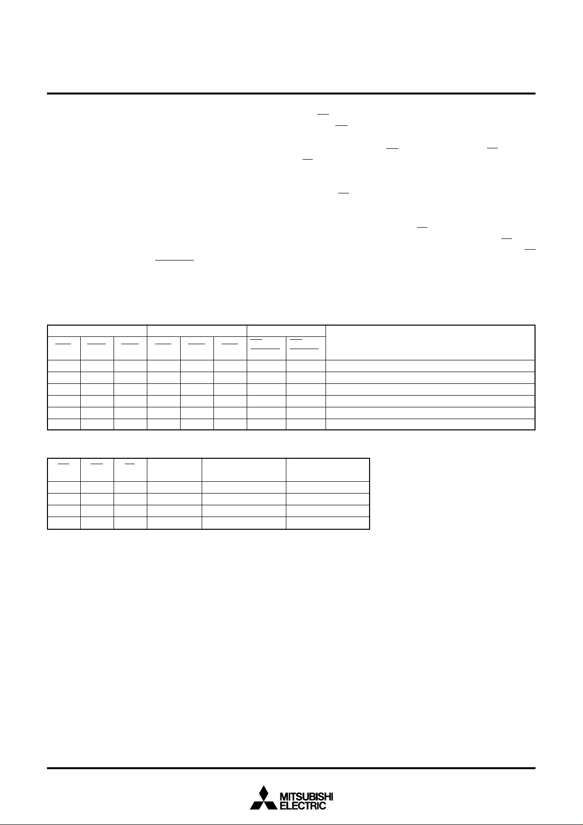
Table 1 Mode Settings of Ports (A0A ~ A7A ≠ A0B ~ A7B)
A port input B port input Flag
CSA
H
×
L
L
×
×
WEA
×
×
L
H
×
×
OEA
×
×
×
L
×
×
CSB
×
H
×
×
L
L
WEB
×
×
×
×
L
H
OEB
×
×
×
×
×
L
Not
Ready A
H
H
H
H
H
H
The CS signal is set to “L” to place one of I/O pins in the input mode.
Also, the WE signal is set to “L”. Data at the I/O pin is thus written
into memory.
As a read operation, the WE signal is set to “H”. Both CS signal and
OE signal are set to “L” to place one of I/O pins in the output mode.
One of addresses A0 to A7 is specified. Data at the specified address
is output to the I/O pin.
When the CS signal is set to “H”, the chip enters a non-select state
which inhibits a read and write operation. At this time, the output is
placed in the floating state (high impedance state), thus allowing OR
tie with another chip. When the OE signal is set to “H”, the output
enters the floating state. In the I/O bus mode, setting the OE signal
to “H” at a write time avoids contention of I/O bus data. When the CS
signal is set to Vcc, the output enters the full stand-by state to minimize
supply current (See Tables 1 and 2).
Not
Ready B
H
H
H
H
H
H
A port is set to the non-select mode.
B port is set to the non-select mode.
A port is set to the write mode for memory.
A port is set to the read mode for memory.
B port is set to the write mode for memory.
B port is set to the read mode for memory.
Operation
Table 2 Basic Functions of Ports
CS
H
Note 1: × indicates “L” or “H”. (Irrelevant)
WE
×
L
L
L
L
H
H
“H” = High level, “L” = Low level
OE
×
×
L
H
Mode
Non-select
Write
Read
I/O pin
High impedance
DIN
DOUT
High impedance
ICC
Stand-by
Operation
Operation
Operation
2
Page 3

MITSUBISHI 〈DIGITAL ASSP〉
M66220SP/FP
256 × 8-BIT MAIL-BOX
FUNCTIONAL DESCRIPTION
Arbitration Function
The M66220 has asynchronous accessibility from two independent
ports to shared memory, thus remarkably improving the throughput
of the entire processor system used in the multiport mode. On the
other hand, this accessibility causes a problem of contending for
selecting the same address in shared memory during the addressing
from both ports.
If the same address is contentionally selected, the following four basic
operations are possible depending on an access mode set from both
ports:
(1) A port .......... Read B port .......... Read
(2) A port .......... Read B port .......... Write
(3) A port .......... Write B port .......... Read
(4) A port .......... Write B port .......... Write
In this case, when both ports are operating in the read mode as given
in (1), correct data is read to both ports and the contents of memory
are not destroyed. There is no special problem. If the other port is in
the read mode while one port is operating in the write mode as given
in (2) or (3), however, data is written correctly but the data read from
the other port in the read mode may change during the same cycle.
This comes into question. When both ports are operating in the write
mode as given in(4), reverse data is written into each port and the
contents of memory may become uncertain. Consequently, no result
will be guaranteed.
The M66220 incorporated an arbitration function circuit to solve such
problems when contentionally selecting an address from both ports.
The arbitration function decides which of A and B ports determines
an address first, and unconditionally assigns access priority to the
first-in port (At this time, the Not Ready signal holds “H”). As for the
last-in port operation, the function inhibits any write to that port from
MPU at the same time when “L” is output to the Not Ready output pin
at the port regardless of a read or write operation during the period of
address matching of both ports. If the address of the first-in port
changes after that and both ports do not have the same address, the
Not Ready output is reset to “H” and the access in the stopped state
is accepted from the last-in port. If the same address is selected by
an address input from both ports simultaneously, a decision by the
arbitration function on the chip also affords access only from one
port, and outputs “L” to the Not Ready output for the other port
invalidate any access from MPU. Tables 3 and 4 give the relationship
between the port arbitration function and port access.
3
Page 4
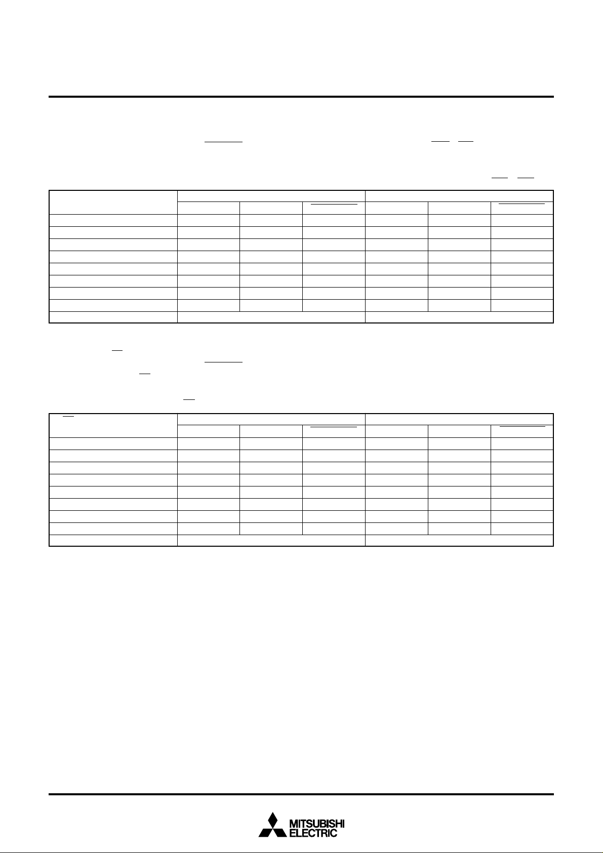
Arbitration Function and Port Access
Contention No.1 (Address control)
Table 3 gives the port access states and the Not Ready signal output
states if the same address is selected in shared memory by an address
MITSUBISHI 〈DIGITAL ASSP〉
M66220SP/FP
256 × 8-BIT MAIL-BOX
input set from A and B ports with CSA = CSB = “L”.
Table 3 Contention Processing by Address Input
Address setting when selecting
same address
First-in A port
First-in B port
First-in A port
First-in B port
First-in A port
First-in B port
First-in A port
First-in B port
Simultaneous A and B ports
Contention No.2 (CS control)
Table 4 gives the port access states and the Not Ready signal output
states when setting the CS inputs from A and B ports valid, and
Table 4 Contention Processing by CS Input
CS input set when selecting
same address
First-in A port
First-in B port
First-in A port
First-in B port
First-in A port
First-in B port
First-in A port
First-in B port
Simultaneous A and B ports
Note 2: “H” = High level, “L” = Low level
Mode setting
Read
Read
Read
Read
Write
Write
Write
Write
Mode setting
Read
Read
Read
Read
Write
Write
Write
Write
A port
Access
,
,
,
,
,
×
,
×
Arbitration Resolved
A port
Access
,
,
,
,
,
×
,
×
Arbitration Resolved
CSA = CSB = “L”
B port
Not Ready A
H
L
H
L
H
L
H
L
selecting the same address in shared memory with A0A to A7A=A0B
to A7B.
Not Ready A
H
L
H
L
H
L
H
L
Mode setting
Read
Read
Write
Write
Read
Read
Write
Write
Mode setting
Read
Read
Write
Write
Read
Read
Write
Write
Access
,
,
×
,
,
,
×
,
Arbitration Resolved
A0A ~ A7A = A0B ~ A7B
B port
Access
,
,
×
,
,
,
×
,
Arbitration Resolved
Not Ready B
L
H
L
H
L
H
L
H
Not Ready B
L
H
L
H
L
H
L
H
4
Page 5

ABSOLUTE MAXIMUM RATINGS (Ta = 0 ~ 70°C, unless otherwise noted)
Symbol
VCC
VI
VO
Pd
Tstg
Supply voltage
Input voltage
Output voltage
Maximum power dissipation
Storage temperature range
Parameter
Conditions
When defining GND pin as a
reference.
Ta = 25°C
RECOMMENDED OPERATING CONDITIONS
Symbol
VCC
GND
VI
Topr
Parameter
Supply voltage
Ground
Input voltage
Operating temperature range
Min.
4.5
0
0
Limits
Typ.
5.0
0
Max.
5.5
VCC
70
MITSUBISHI 〈DIGITAL ASSP〉
M66220SP/FP
256 × 8-BIT MAIL-BOX
Ratings
–0.3 ~ +7.0
–0.3 ~ VCC + 0.3
0 ~ VCC
700
–65 ~ 150
Unit
V
V
V
°C
Unit
V
V
V
mW
°C
ELECTRICAL CHARACTERISTICS (Ta = 0 ~ 70°C, Vcc=5V±10%, unless otherwise noted)
Symbol
VIH
VIL
VOH
VOL
VOL
IIH
IIL
IOZH
IOZL
ICC
ISB1
ISB2
ISB3
“H” input voltage
“L” input voltage
“H” output voltage (I/O)
“L” output voltage (I/O)
Open drain “L” output voltage (Not Ready)
“H” input current
“L” input current
Off state “H” output current
Off state “L” output current
Static current dissipation (active)
Two-port stand-by
One-port stand-by
Two-port full stand-by
Parameter
Test conditions
IOH = –2mA
IOL = 4mA
IOL = 8mA
VI = VCC
VI = GND
CS = VIH or OE = VIH
VO = VCC
CS = VIH or OE = VIH
VO = GND
CS < 0.2V,
Another input VIN > VCC – 0.2V
or VIN < 0.2V, Output pin open
CSA, CSB = VIH
CSA or CSB = VIH
IOUT = 0mA
(Active port output pin open)
CSA, CSB > VCC – 0.2V
Another input VIN > VCC – 0.2V
or VIN < 0.2V
Min.
2.2
–0.3
2.4
Limits
Typ.
Max.
VCC+0.3
0.8
0.5
0.5
10.0
–10.0
10.0
–10.0
60
5
60
0.1
Unit
V
V
V
V
V
µA
µA
µA
µA
mA
mA
mA
mA
Stand-by current
ISB4
CI
CO
Notes 3: The direction in which current flows into the IC is defined as positive (no sign).
4: The above typical values are standard values for V
One-port full stand-by
Input capacitance
Output capacitance in off state
CC = 5V and Ta = 25°C.
CSA or CSB > VCC – 0.2V
Another input VIN > VCC – 0.2V
or VIN < 0.2V, IOUT = 0mA
(Active port output pin open)
30
10
15
mA
pF
pF
5
Page 6

MITSUBISHI 〈DIGITAL ASSP〉
SWITCHING CHARACTERISTICS (Ta = 0 ~ 70°C, VCC = 5V±10%, unless otherwise noted)
Read cycle
Symbol
tCR
ta(A)
ta(CS)
ta(OE)
tdis(CS)
tdis(OE)
ten(CS)
ten(OE)
tv(A)
Read cycle time
Address access time
Chip select access time
Output enable access time
Output disable time after CS (Note 5)
Output disable time after OE (Note 5)
Output enable time after CS (Note 5)
Output enable time after OE (Note 5)
Data effective time after Address
Parameter
Min.
70
5
5
10
TIMING REQUIREMENTS (Ta = 0 ~ 70°C, VCC = 5V±10%, unless otherwise noted)
Write cycle
Symbol
tCW
tw(WE)
tsu(A)
tsu(A-WEH)
tsu(CS)
tsu(D)
th(D)
trec(WE)
tdis(WE)
tdis(OE)
ten(WE)
Note 5: The time required for the output to change from a steady state to ±500mV under the load conditions shown in Fig 2.
This parameter is guaranteed but is not tested at shipment.
Write cycle time
Write pulse width
Address setup time
Address setup time for rise of WE.
Chip select setup time (for WE)
Data setup time
Data hold time
Write recovery time
Output disable time after WE (Note 5)
Output disable time after OE (Note 5)
Output enable time after WE (Note 5)
Parameter
Min.
70
45
0
65
65
40
0
0
0
M66220SP/FP
256 × 8-BIT MAIL-BOX
Limits
Typ. Max.
70
70
35
35
35
Limits
Typ. Max.
35
35
Unit
ns
ns
ns
ns
ns
ns
ns
ns
ns
Unit
ns
ns
ns
ns
ns
ns
ns
ns
ns
ns
ns
NOT READY TIMING (Ta = 0 ~ 70°C, VCC = 5V±10%, unless otherwise noted)
6
tNAA
tNDA
tNAC
tNDC
tAPS
tNO
tNW
Symbol
Not Ready access time from Address
Not Ready disable time from Address
Not Ready access time from CS
Not Ready disable time from CS
Arbitration priority setup time
Data output access time from Not Ready.
Write hold time from Not Ready.
Parameter
Min.
15
65
Limits
Typ. Max.
50
50
50
50
Unit
ns
ns
ns
ns
ns
0
ns
ns
Page 7

TIMING DIAGRAM
Read Cycle (WE = V
Read cycle No.1 (Address control) (CS = OE = VIL)
0~A7
A
I/O0~I/O
7
(D
OUT
)
Read cycle No.2 (CS control)
IH)
t
v(A)
Previous cycle data Data output determined
t
a(A)
MITSUBISHI 〈DIGITAL ASSP〉
M66220SP/FP
256 × 8-BIT MAIL-BOX
CR
t
t
v(A)
A
0~A7
CS
OE
I/O0~I/O7
(DOUT)
High impedance
t
CR
ta(A)
ta(CS) tdis(CS)
ten(CS)
ta(OE)
ten(OE)
Data output determined
tdis(OE)
7
Page 8

Write Cycle
Write cycle No.1 (WE control) See Notes 6, 7 and 8.
0~A7
A
CS
t
su(A)
WE
t
su(A-WEH)
t
CW
t
su(CS)
w(WE)
t
t
su(D)
t
rec(WE)
t
MITSUBISHI 〈DIGITAL ASSP〉
M66220SP/FP
256 × 8-BIT MAIL-BOX
h(D)
I/O0~I/O
7
(DIN)
OE
t
dis(OE)
I/O0~I/O
7
(D
OUT
)
Write cycle No.2 (CS control) See Notes 6, 7 and 8.
A0~A
7
t
su(A-WEH)
t
su(A)
CS
WE
t
CW
t
su(CS)
Data input determined
t
w(WE)
t
rec(WE)
8
I/O0~I/O
(DIN)
I/O0~I/O
(D
OUT
t
t
su(D)
7
t
en(CS)
7
t
dis(WE)
Data input determined
h(D)
)
Notes 6:
The WE of the port must be set to “H” when an address input changes.
A write operation is performed during the overlap period when both CS and WE are “L”.
7:
Do not apply any negative-phase signal from outside when an I/O pin is in output state.
8:
The shaded part means a state in which a signal can be “H” or “L”.
9:
Page 9

Contention Read Cycle (WE = VIH, OE = VIL)
Contention read cycle No.1 (Address control) See Notes 10 and 11.
MITSUBISHI 〈DIGITAL ASSP〉
M66220SP/FP
256 × 8-BIT MAIL-BOX
Address A
(Address B)
Address B
(Address A)
∗ Address matching Address not matching
t
APS
∗
t
NAA
Not Ready B
(Not Ready A)
t
v(A)
I/O0B~I/O7B
(I/O
0
A~I/O7A)
Previous cycle data
∗ Address A = Address B
Contention read cycle No.2 (CS control) See Notes 10 and 12.
Addresses
A & B
t
a(A)
∗ Address matching
t
NDA
t
NO
Data output determined
CSA
(CSB)
CSB
(CSA)
Not Ready B
(Not Ready A)
I/O0B~I/O7B
0
A~I/O7A)
(I/O
t
APS
t
NAC
t
en(CS)
∗ Address A = Address B
Notes 10: The Not Ready output of the first-in port holds “H”.
When CS is set to “L” before the address input is determined.
11:
When the address input is determined before CS transition to “L”.
12:
t
a(CS)
t
NDC
t
NO
Data output determined
9
Page 10

Contention Write Cycle
Contention write cycle No.1 (WE control) See Notes 6, 8, 10 and 11.
Address A
(Address B)
∗ Address matching
tAPS
MITSUBISHI 〈DIGITAL ASSP〉
M66220SP/FP
256 × 8-BIT MAIL-BOX
Address B
(Address A)
t
NAA
∗
Not Ready B
(Not Ready A)
tsu(A)
WEB
(WEA)
I/O0B~I/O7B
(I/O
0A~I/O7A)
(D
IN)
tdis(WE)
I/O0B~I/O7B
(I/O
0A~I/O7A)
(D
OUT)
∗ Address A = Address B
Contention write cycle No.2 (CS control) See Notes 6, 8, 10 and 12.
Addresses
A & B
∗ Address matching
su(A-WEH)
t
tNDA
tNW
tw(WE)
tsu(D) th(D)
Data input determined
ten(WE)
CSA
(CSB)
CSB
(CSA)
Not Ready B
(Not Ready A)
WEB
(WEA)
I/O0B~I/O7B
(I/O
0
A~I/O7A)
(D
IN
I/O0B~I/O7B
(I/O
0
A~I/O7A)
(D
OUT
t
APS
t
NAC
t
su(CS)
t
NDC
t
NW
tw
(WE)
su(D)
t
t
h(D)
Data input determined
)
t
en(CS)
t
dis(WE)
t
en(WE)
)
∗ Address A = Address B
10
Page 11

MITSUBISHI 〈DIGITAL ASSP〉
M66220SP/FP
256 × 8-BIT MAIL-BOX
SWITCHING CHARACTERISTICS MEASUREMENT CIRCUIT
Input pulse level : VIH = 3.0V, VIL = 0V
Input pulse rise/fall time : tr/tf = 5ns
Input timing reference voltage : 1.5V
Output timing decision voltage : 1.5V
Output load : Figure 1 ~ 3 (The capacitance includes stray wiring capacitance and the probe input capacitance.)
+
5V
1250Ω
I/O
100pF775Ω
Fig 1. I/O Output Load Fig 2. I/O Output Load
I/O
(to ten, tdis)
++
5V
1250Ω
Not Ready
5pF775Ω
Fig 3. Not Ready Output Load
5V
575Ω
50pF
11
 Loading...