

Page 1
MITSUBISHI 〈DIGITAL ASSP〉
MITSUBISHI 〈DIGITAL ASSP〉
DESCRIPTION
The M66004 is a 16-digit 5×7-segment vacuum fluorescent
display (VFD) controller using the silicon gate CMOS technology.
It contains 160 ROM characters and 16 user-defined RAM
characters and receives display character codes and various
commands from MCU to control VFD.
FEATURES
• Built in 5×7-dot segment character ROM
(160 characters based on JIS-C-6220. Customization is
possible.)
• Built in character RAM for user definition (16 characters)
• Display digit length can be changed. (from 9 to 16 digits)
• One-digit display cycle setting can be changed. (2 cycles)
• Dimmer is adjustable. (8 grades)
• Cursor display ON or OFF is selectable. (SEG
35 output)
• Built in automatic display digit increment function
• Auto increment of display digit
• Built in simultaneous all-digit display ON/OFF command
• Connection to MCU by three signal lines, CS, SCK and
SDATA
• Instruction execution with one byte*
• 2 general purpose output ports
• Positive supply voltage V
• Pull-down voltage V
V
CC=5V ± 10%
P=VCC-40V typ.
CC-45V max. (peak)
*: Except for character RAM setting
APPLICATION
AV equipments, vacuum fluorescent display controller for
POS system, etc.
FUNCTION
The M66004 is a 16-digit 5×7-segment VFD (Vacuum Fluorescent Display) controller and contains 160 ROM characters
based on JIS-C-6220 which can be customized and 16 RAM
characters that user can define freely.
Character display codes and various commands are received as 8-bit serial data from MCU.
Main functions of this IC are display digit length setting, onedigit display cycle setting and dimmer adjustment.
It has 36 segment output pins from SEG
uses 35 pins from SEG
35 output, which is independent of other segment, is
SEG
00 to SEG34 for character display.
00 to SEG35 and
used for cursor display by inputting either cursor ON or OFF
command.
Once display data is fixed, display continues automatically
until new data is input. Therefore, MCU can execute other
jobs and is lightened of its load.
Additionally , the IC can control other I/O elements because it
contains two static operation output ports.
16-DIGIT 5X7-SEGMENT VFD CONTROLLER
16-DIGIT 5×7-SEGMENT VFD CONTROLLER
DIG11 DIG12
DIG10
DIG
DIG
DIG
Digit outputs
Reset input
Chip select input
Shift clock input
Serial data input
Output ports
Clock output
Clock input
Segment outputs
DIG
DIG
DIG
DIG
DIG
DIG01 ←11
DIG00 ←12
RESET →13
SDATA →16
SEG35 ←23
SEG34 ←24
SEG33 ←25
SEG32 ←26
SEG31 ←27
SEG30 ←28
SEG29 ←29
SEG28 ←30
SEG27 ←31
M66004SP/FP
1
←
2
←
09
3
←
08
4
←
07
5
←
06
6
←
05
7
←
04
8
←
03
9
←
02
10
CS →14
CSK →15
P1 ←17
P0 ←18
VCC1
19
XOUT ←20
XIN →21
VSS
22
VP
32
M66004SP/FP
→←
64
→
→
→
→
→
→
→
→
→
→
→
→
→
→
→
→
→
→
→
→
→
→
→
→
→
→
→
→
→
→
DIG
DIG
DIG
VCC2
SEG
SEG
SEG
SEG
SEG
SEG
SEG
SEG
SEG
SEG
SEG
SEG
SEG
SEG
SEG
SEG
SEG
SEG
SEG
SEG
SEG
SEG
SEG
SEG
SEG
SEG
SEG
13
14
15
00
01
02
03
04
05
06
07
08
09
10
11
12
13
14
15
16
17
18
19
20
21
22
23
24
25
26
63
62
61
60
59
58
57
56
55
54
53
M66004SP/FP
52
51
50
49
48
47
46
45
44
43
42
41
40
39
38
37
36
35
34
33
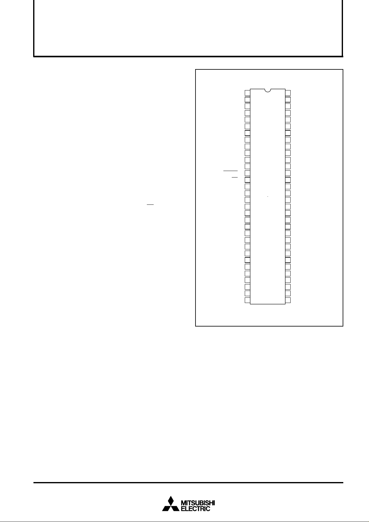
Outline 64P4B
64P2G-A
Digit output
Segment outputs
1
Page 2
BLOCK DIAGRAM
MITSUBISHI 〈DIGITAL ASSP〉
M66004SP/FP
16-DIGIT 5×7-SEGMENT VFD CONTROLLER
Chip
select input
Shift
clock input
Serial
data input
Reset
input
Clock
input
Clock
output
CS
RESET
OUT
Display code register
(8-bit × 16)
code
write
14
15SCK
16SDATA
13
21X
IN
20X
Serial
receive circuit
Clock
generator
Code /
command
control circuit
Display control
register
RAM
write
code select
Display controller
(35-bit × 160)
DecoderDecoder
(35-bit × 16)
CGROM
CGRAM
Segment
output circuit
Output port
(2 bits)
Digit
output circuit
59 SEG
33 SEG
SEG
31
23
SEG
P
0
18
P
1
17
DIG
12
DIG
1
64
DIG
61
DIG
00
26
27
35
00
11
12
15
Segment
outputs
Output
ports
Digit
outputs
OPERATION FLOW
The serial receive circuit receives 8-bit serial data, latches
the data by an internal latch signal, and then masks inputs
from the MCU.
When the code/command circuit receives a command, it sets
the display control register to the fixed state, and when it receives a character code, it writes the code to one of 16 display code registers which corresponds to the digit to display.
The display controller outputs digit ON/OFF timing pulse to
the digit output circuit and selects one character code to display among display code registers. The selected character
code is input to either CGROM decoder or CGRAM decoder
and then converted into a 35-bit character pattern to input the
segment output circuit.
2
Page 3
PIN DESCRIPTIONS
Symbol
Pin name
MITSUBISHI 〈DIGITAL ASSP〉
M66004SP/FP
16-DIGIT 5X7-SEGMENT VFD CONTROLLER
Function
RESET
CS
SCK
SDATA
XIN,
XOUT
DIG00~
DIG15
SEG00~
SEG35
P0, P1
VCC1
VCC2
VSS
VP
Reset input
Chip select
input
Shift clock
input
Serial data
input
Clock input
Clock output
Digit output
Segment
output
This pin is used to initialize the internal state of the M66004.
In “L” state, communication with the MCU is possible.
In “H” state, any instruction from the MCU is neglected.
At the rising edge from “L” to “H”, input data is shifted.
Character code or command data to display is input from MSB.
This pin is used to connect a resistor and a capacitor externally to set oscillation frequency. (maximum
oscillation frequency fosc(max)=1MHz) An external clock can be also connected. In this case, an external
clock is connected to pin XIN, and pin XOUT is set to be in open state.
These pins are used to connect to digit pins of VFD. Pins from DIG00 to DIG15 correspond to digits of VFD
from the first digit to the 16th digit.
These pins are used to connect to segment pins of VFD. Pins from SEG00 to SEG35 correspond to segment
pins of VFD as shown in the table below.
Output port (static operation)
Positive power supply for internal logic
Positive power supply for high-pressure-resistant output port
GND
Negative power supply for VFD drive
(Connection of segment output pins)
Each in the table shows one-dot segment and each figure
in shows the output segment pin number (from 00 to 35) to
connect.
00 01 02 03 04
05 06 07 08 09
10 11 12 13 14
15 16 17 18 19
20 21 22 23 24
25 26 27 28 29
30 31 32 33 34
35
3
Page 4
MITSUBISHI 〈DIGITAL ASSP〉
M66004SP/FP
16-DIGIT 5×7-SEGMENT VFD CONTROLLER
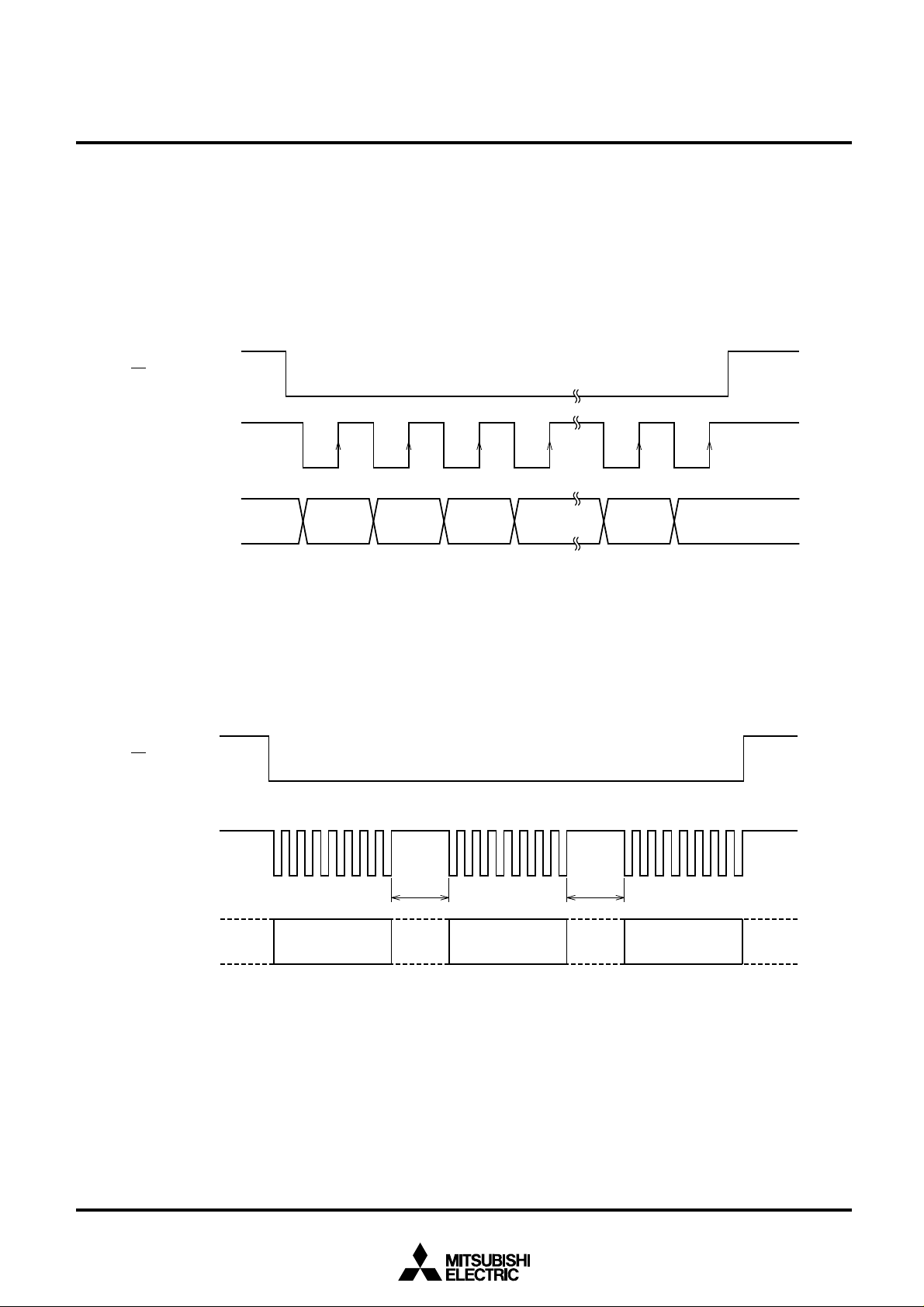
DATA TRANSMISSION FORMAT
The MCU transmits 8-bit serial data (MSB-first) to the
M66004. In either case of command data or character code
data, the M66004 operates by transmitting only one-byte
data.
(Transmission timing)
Standard timing
CS
SCK
SDATA D7 D6
(MSB)
However, in case of character RAM data setting, it is necessary to send 7-byte data continuously.
D5 D4 D1
D0
(LSB)
Continuous data transmission timing (In the following example, command data is transmitted and then character
codes are transmitted continuously.)
CS
SCK
t
SDATA Command data
BUSY
: Internal processing time
t
BUSY
Character code Character code
t
BUSY
4
Page 5
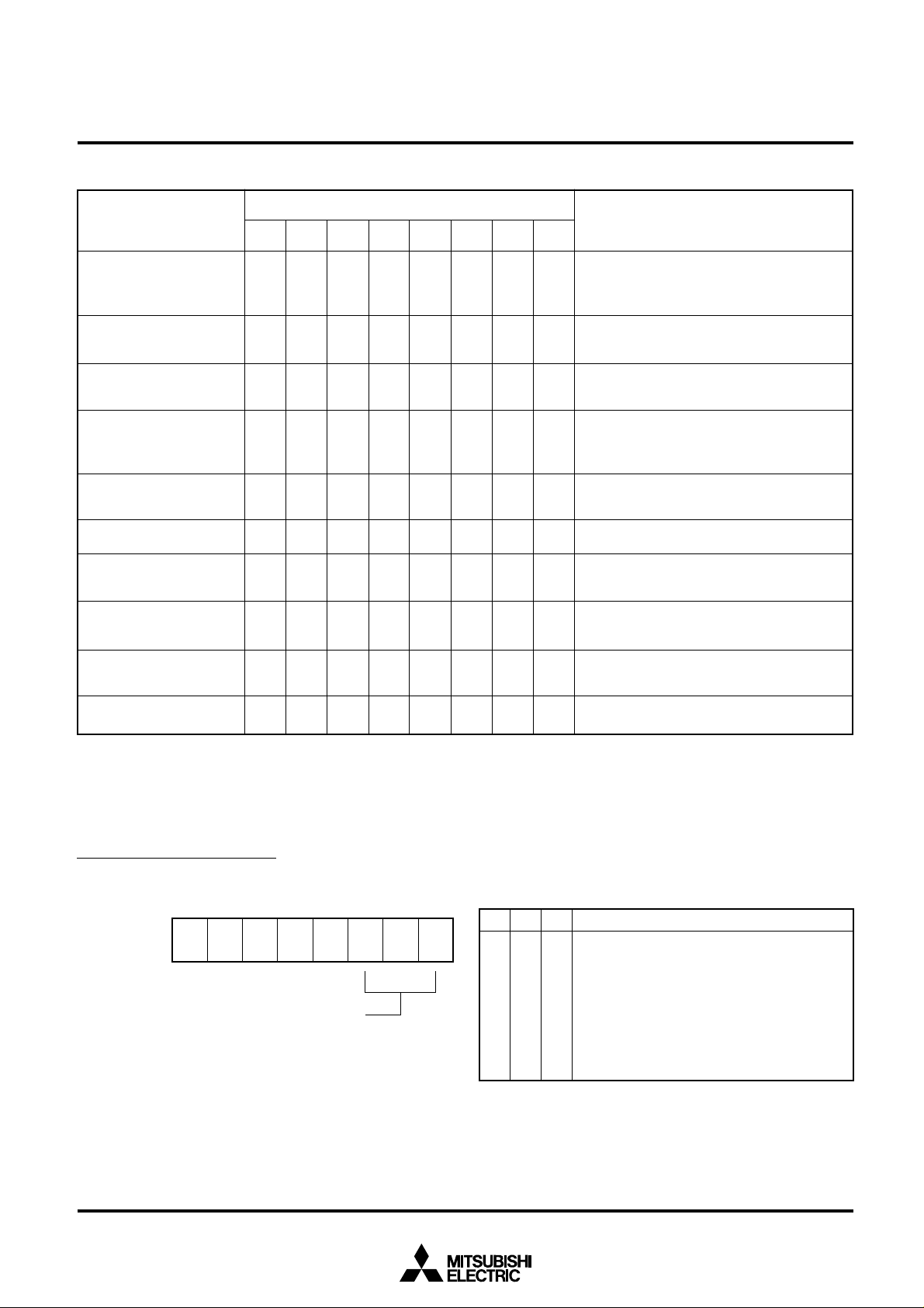
COMMAND LIST
MITSUBISHI 〈DIGITAL ASSP〉
M66004SP/FP
16-DIGIT 5X7-SEGMENT VFD CONTROLLER
Function
Display digit length setting
Dimmer value setting
One-digit display frequency
setting
Display digit setting
Auto increment setting
Cursor ON
Cursor OFF
All digit display ON/OFF
D7
Command code
D0
D1
D2
D3
D4
D5
D6
The number of digits to display is fixed. Eight
0
0
1
1
1
0
1
1
0
0
0
0
1
1
1
1
1
1
0
0
0
0
1
1
0
0
1
0
0
1
*
0
0
1
*
1
*
0
0
1
*
*
*
*
1
1
*
*
0
1
*
*
*
*
*
0
types of setting (from 9 digits to 16 digits) are
*
possible.
Eight types of setting (from 1/16 to 14/16) are
*
possible for dimmer value.
Either 128/fOSC or 256/fOSC is selected as one-
*
digit display frequency.
The first character code received after
*
executing this command is displayed as
designated by this command.
This command is executed to set or cancel the
*
automatic display digit increment function.
This command is executed to make SEG35 ON.
*
This command is executed to make SEG35
*
OFF.
This command is executed to make all-digit
*
display OFF or all-digit/segment display ON.
Contents
Write to user RAM
Output port state setting
×: Optional
*: Refer to the description of command.
1
1
DESCRIPTION OF COMMAND
1. Display digit length setting
D7 D6 D5 D4 D3 D2 D1 D0
00000
Display digit length (See table 1.)
1
*
0
1
1
1
1
definition.
Output ports P0 and P1 are set or reset.
*
Character data is written into RAM for user
×
×
1
1
1
1
Table 1 Display digit length
D2
D1
D0
0
0
0
0
0
1
0
1
0
0
1
1
1
0
0
1
0
1
1
1
0
1
1
1
Display digit length
9
10
11
12
13
14
15
16
5
Page 6

2.
Setting of dimmer value and one-digit display frequency(T
dsp
1) Dimmer value setting
D7 D6 D5 D4 D3 D2 D1 D0
00001
Dimmer value (See table 2.)
2) One-digit display frequency (Tdsp) setting
16-DIGIT 5×7-SEGMENT VFD CONTROLLER
)
Table 2 Dimmer value
D2
D1
D0
0
0
0
0
0
1
1
1
1
Tdig : One-digit-ON pulse width
dsp: One-digit display frequency
T
0
0
1
1
0
1
1
0
0
0
1
1
0
1
1
4. All-digit display ON/OFF
MITSUBISHI 〈DIGITAL ASSP〉
M66004SP/FP
Dimmer value (Tdig/Tdsp)
1/16
2/16
4/16
6/16
8/16
10/16
12/16
14/16
D7 D6 D5 D4 D3 D2 D1 D0
1111 110
One-digit display frequency (Tdsp)
0: Tdsp=128/fOSC
1: Tdsp=256/fOSC
3.
Display digit setting, setting and cancel of auto increment
1) Display digit setting
D7 D6 D5 D4 D3 D2 D1 D0
1110
Display digit (Note 1)
2) Setting and cancel of auto increment
D7 D6 D5 D4 D3 D2 D1 D0
D7 D6 D5 D4 D3 D2 D1 D0
1111 00
Table 3 ON/OFF control
D1
D0
×
0
0
1
1
1
×: Don’t care
All-digit display OFF (All-OFF)
Normal operation mode setting
All-digit/segment display ON (All-ON)
Operation
5. Cursor OFF (SEG35 output OFF)
D7 D6 D5 D4 D3 D2 D1 D0
1000
Digit setting (Note 2)
See table 3.
1111 100
Setting and cancel of auto increment
1: Setting of auto increment
0: Cancel of auto increment
Note 1: When the display digit is defined as N, N equals [decimal values to
which D3, D2, D1 and D0 are converted + 1]. In case of (D3, D2, D1,
D0)=(1, 0, 0, 0), N is 9. The first character code received after executing this command is despoiled to the 9th digit.
6
6. Cursor ON (SEG35 output ON)
D7 D6 D5 D4 D3 D2 D1 D0
0001
Digit setting (Note 2)
Note 2: The digit to which the cursor to make display ON or OFF belongs is
designated. When digit is defined as N, N equals [decimal values to
which D3, D2, D1 and D0 are converted + 1]. In case of (D3, D2, D1,
D0)=(1, 0, 0, 0), N is 9. ON/OFF control of the cursor which belongs
to the 9th digit is possible.
Page 7

MITSUBISHI 〈DIGITAL ASSP〉
M66004SP/FP
16-DIGIT 5X7-SEGMENT VFD CONTROLLER
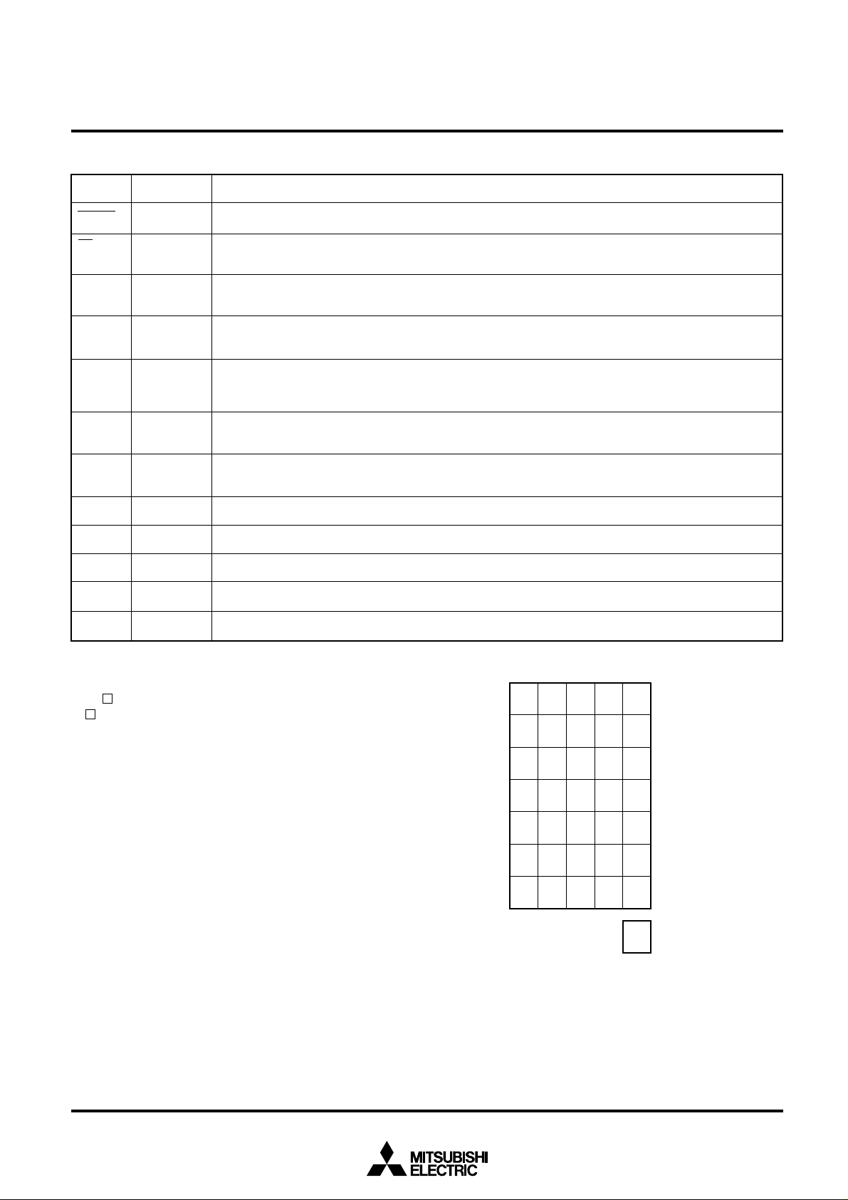
7. Write to character RAM for user definition
Segment ON/OFF data is written into the character RAM for
user definition (35 bits). After write to RAM is declared at the
first byte, RAM is selected at the second byte and ON/OFF
data is transmitted at the 3rd to 7th byte. Therefore, write to
RAM is executed by a 7-byte command.
Character codes from RAM1 to RAM 16 are assigned to data
from 90
1st byte
(Declaration of
write to RAM)
2nd byte
(Selection of RAM)
16 to 9F16 respectively.
D7 D6 D5 D4 D3 D2 D1 D0
111111××
D7 D6 D5 D4 D3 D2 D1 D0
× ×××
RAM selection
RAM 1 : (D3, D2, D1, D0) = (0, 0, 0, 0)
~
RAM 16: (D3, D2, D1, D0) = (1, 1, 1, 1)
× : Don’t care
~
~
× : Don’t care
1st column 3rd column 5th column
00 01 02 03 04
05 06 07 08 09
10 11 12 13 14
15 16 17 18 19
20 21 22 23 24
25 26 27 28 29
30 31 32 33 34
2nd column 4th column
(Segment number)
Ex. In order to define “F” (see the figure) as
character RAM 1, 7-byte data as shown
in the following table should be
transmitted in serial order.
3rd byte (Data
in 1st column)
4th byte (Data
in 2nd column)
5th byte (Data
in 3rd column)
6th byte (Data
in 4th column)
7th byte (Data
in 5th column)
D7 D6 D5 D4 D3 D2 D1 D0
00 05 10 15 20 25 30 ×
01 06 11 16 21 26 31 ×
02 07 12 17 22 27 32 ×
03 08 13 18 23 28 33 ×
04 09 14 19 24 29 34 ×
0: corresponding segment OFF
1: corresponding segment ON
Transmission data
1
2
3
4
5
6
7
All optional bits are set to “0”.
FC16
0016
FE16
9016
9016
9016
8016
Declaration of write to RAM 1
Selection of RAM 1
Setting of 1st-column segment data
Setting of 2nd-column segment data
Setting of 3rd-column segment data
Setting of 4th-column segment data
Setting of 5th-column segment data
8. Output port setting
D7 D6 D5 D4 D3 D2 D1 D0
111110
Remarks
P0 set/reset
P1 set/reset
Set (“H”): 1
Reset (“L”): 0
7
Page 8

MITSUBISHI 〈DIGITAL ASSP〉
M66004SP/FP
16-DIGIT 5×7-SEGMENT VFD CONTROLLER
DESCRIPTION OF FUNCTION
1. Display digit length setting
The display digit length can be set within the range from 9digit to 16-digit according to the number of digits of VFD.
In case that the display digit length is set to 12 when a 16digit VFD is used, digits from 13 to 16 are displayed as blank.
2. Dimmer value and one-digit display frequency (T
dsp)
setting
Regarding dimmer value, 8-stage setting is possible. One-
DISPLAY TIMING
T
dsp
blk
T
Digit N
(Most significant digit)
digit display scan time (T
OSC or Tdsp=256/fOSC.
f
dsp) can be set to either Tdsp=128/
Scan cycle time T is set to T=T
length).
Ex. fOSC=455kHz, N=16
dsp=281µs, T=4.5ms (222Hz) or Tdsp=562µs, T=9.0ms (111Hz)
T
T
dsp × N (N: display digit
Digit N-1
Digit N-2
•
•
•
•
•
Digit 1
(Least significant digit)
T
dig
T: Scan cycle time
T
dig
: One-digit-ON pulse width
T
dsp
: One-digit scan time
T
blk
: Blanking time
8
Page 9

MITSUBISHI 〈DIGITAL ASSP〉
M66004SP/FP
16-DIGIT 5X7-SEGMENT VFD CONTROLLER
3. Character display
A character (refer to the character code table) which corresponds to the character code transmitted from the MCU is
displayed as the designated digit.
The display digit is designated by the display digit setting
command. In case that the display digit designated by this
command is set to increase automatically , the display digit is
automatically increased by 1. After a character is displayed to
the most significant digit, it is displayed to the least significant
digit.
When the auto increment setting is canceled, the display digit
is fixed.
Ex. In order to display a character A to digits 14, 15, 16, 1 and 2 in this order
and characters A, B and C to digit 8 successively, 12-byte data must be
transmitted in the following order.
Transmission data
1
2
3
4
5
6
7
8
9
10
11
12
F516
ED16
4116
4116
4116
4116
4116
F416
E716
4116
4216
4316
Display digit
–
–
14
15
16
1
2
–
–
8
8
8
(Display digit length = 16)
A (code 41
B (code 42
C (code 43
Remarks
Setting of auto increment
Display digit is set to the
14th digit.
Transmission of
character code
Cancel of auto increment
setting
Display digit is set to the 8th
digit.
Transmission of
character code
16)
16)
16)
OPERATION AT RESET
When a reset signal is input, the internal state is initialized as
shown in Table 4.
Table 4 Initial state
Contents
Display (characters and cursor)
Display digit length, dimmer value,
display digit, one-digit display frequency,
user character RAM state, auto increment setting
Serial receive circuit
Output port setting
Setting after reset
All digits: OFF
Values immediately
before reset are
held.
Reset
Set
4. All-digit display ON/OFF
All digits are simultaneously lighted or put off by inputting alldigit display ON command or all-digit display OFF command.
When all-digit display ON command is transmitted, all digits
including a cursor and all segments are lighted.
Therefore, this command can be used for the lamp test.
When all-digit display ON setting is canceled (normal operation mode is selected), all digits are displayed according to
the setting before all-digit display ON operation. It is also
possible to set the next character to the designated digit during the all-digit display ON operation.
When all-digit display OFF command is transmitted, all digits
including a cursor are put off. When all-digit display OFF setting is canceled (normal operation mode is selected), all digits are displayed according to the setting before all-digit
display OFF operation. It is also possible to set the next character to the designated digit in the all-digit display OFF state.
9
Page 10

MITSUBISHI 〈DIGITAL ASSP〉
16-DIGIT 5×7-SEGMENT VFD CONTROLLER
ABSOLUTE MAXIMUM RATINGS
Symbol
VCC
VP
VI
VO
Pd
Tstg
Notes 3: Frequency of pulse waveform exceeding VCC-40V:450µs or above, pulse width: 30µs or below, output load: CL≤200pF
4: When T
5: When T
Supply voltage
Pull-down voltage
Input voltage
Output voltage
Maximum power dissipation
Storage temperature
a is 25°C or above, derating (12.8mW/°C) should be conducted.
a is 25°C or above, derating (11.2mW/°C) should be conducted.
Parameter
VCC1, VCC2
XOUT, P0, P1
SP
FP
Conditions
(Note 3)
Any external circuits are
not connected to the IC.
Ta=25°C (Note 4)
The IC is mounted on a
board. Ta=25°C (Note 5)
–0.3 ~ + 7
VCC–45 ~ VCC + 0.3
–0.3 ~ VCC + 0.3
–0.3 ~ VCC + 0.3
–65 ~ 150
M66004SP/FP
Ratings
1.6
1.4
Unit
V
V
V
V
W
°C
RECOMMENDED OPERATIONAL CONDITIONS (Ta=–10 ~ 70°C unless otherwise noted)
VCC
VP
VSS
VI
Topr
Symbol
Supply voltage
Pull-down voltage
Supply voltage
Input voltage
Operating temperature
Parameter
Conditions
VCC1, VCC2
DC CHARACTERISTICS (Ta = –10 ~ 70°C, VCC = 5V ± 10%, VSS = 0V)
Symbol
VIH
VIL
VT+
VT–
IIH
IIL
VOH
VOL
IO
ICC
(Note 6)
IP
Note 6: Total of current at pin VCC1 and current at pin VCC2.
“H” input voltage
“L” input voltage
Positive direction
threshold voltage
Negative direction
threshold voltage
“H” input current
“L” input current
“H” output voltage
“L” output voltage
Output pull-down current
Positive supply current
Negative supply current
Parameter
SDATA
RESET
CS
SCK, XIN
DIG output
SEG output
P0, P1
P0, P1
DIG, SEG
VCC1, VCC2
VP
Conditions
VI=VCC
VI=0V
IOH=–20mA
IOH=–5mA
IOH=–2mA
IOL=2mA
VP=VCC–40V, VO=VCC
VI=0V, Output pin: open
VP=VCC–40V
Output pin: open
Output “H”, clock stop
VP=VCC–40V
Output pin: open
Output “H”, clock stop
VP=VCC–40V
Min.
4.5
VCC–40
0
–10
Min.
0.7VCC
0.35VCC
0.2VCC
VCC–2
VCC–2
VCC–0.8
250
Limits
Typ.
5
0
Limits
Typ.
2.8
2
500
Max.
5.5
VCC
VCC
70
Max.
0.3VCC
0.7VCC
0.55VCC
1
–1
0.55
850
100
40
–40
Unit
V
V
V
V
°C
Unit
V
V
V
V
µA
µA
V
V
µA
µA
mA
mA
10
Page 11

MITSUBISHI 〈DIGITAL ASSP〉
M66004SP/FP
16-DIGIT 5X7-SEGMENT VFD CONTROLLER
TIMING CONDITIONS (Ta = –10 ~ 70°C, VCC = 5V ± 10%, VSS = 0V)
Symbol
tC
tWH
tWL
tsu(D)
th(D)
tsu(CS)
th(CS)
tBUSY (Note 7)
Note 7: This shows the internal operation time after receiving the serial data. Next data is prohibited in this period. Next data is available after 6T of the operation
clock.
Clock cycle time
Clock cycle pulse width
Clock low pulse width
SDATA setup time
SDATA hold time
CS setup time
CS hold time
Internal processing time
Parameter
SCK
XIN
SCK
XIN
SCK
XIN
Conditions
Min.
500
1000
230
460
230
460
130
100
130
Limits
Typ. Max.
Unit
ns
ns
ns
ns
ns
0
ns
ns
6
1/fOSC
OSCILLATION CHARACTERISTICS (Ta = –10 ~ 70°C, VCC = 5V ± 10%, VSS = 0V)
Conditions
C=100pF, R=27kΩ
fOSC
Symbol
Parameter
Oscillation frequency
TIMING WAVEFORM (Reference voltage: 0.3VCC, 0.7VCC)
CS
tC
t
SCK
SDATA
su(CS)
tWL
tsu(D) th(D)
t
WH
Limits
Min. Typ.
500
th(CS)
Max.
Unit
kHz
SCK
tBUSY
nth byte (n+1)th byte
11
Page 12

OPERATION FLOWCHART (Initial setting operation)
ONE-DIGIT DISPLAY FREQUENCY
MITSUBISHI 〈DIGITAL ASSP〉
M66004SP/FP
16-DIGIT 5×7-SEGMENT VFD CONTROLLER
START
PUT OFF ALL-
DIGIT DISPLAY
SET DISPLAY DIGIT LENGTH
SET DIMMER VALUE AND
TRANSMIT RAM WRITE COMMAND
TRANSMIT RAM BIT DATA
NO
BIT DATA TRANSMISSION COMPLETED
YES
NO
WRITE TO RAM COMPLETED
YES
SET AUTO INCREMENT,
SET DISPLAY DIGIT
TRANSMIT DISPLAY CHARACTER CODE
12
NO
TRANSMISSION OF ALL DIGITS COMPLETED
YES
SET TO NORMAL OPERATION MODE
END
Page 13

CHARACTER CODE LIST (conforming to JIS-C-6220)
Lower codes
Upper codes
0000
(0
16)
0001
(1
16)
0010
(2
16)
0011
(316)
0100
16)
(4
0101
(5
16)
0110
16)
(6
0111
(716)
MITSUBISHI 〈DIGITAL ASSP〉
M66004SP/FP
16-DIGIT 5X7-SEGMENT VFD CONTROLLER
1000
(8
16)
1001
(9
16)
1010
(A
16)
1011
(B16)
1100
(C16)
1101
16)
(D
1110
(E
16)
1111
(F
16)
0000
16)
(0
0001
(1
16)
0010
(2
16)
0011
(3
16)
0100
(4
16)
0101
(5
16)
0110
(6
16)
0111
(7
16)
SPASE
RAM1
RAM2
RAM3
RAM4
RAM5
RAM6
RAM7
RAM8
SPASE
1000
(8
16)
1001
(9
16)
1010
(A
16)
1011
(B
16)
1100
(C
16)
1101
(D
16)
1110
(E
16)
1111
(F
16)
RAM9
RAM10
RAM11
RAM12
RAM13
RAM14
RAM15
RAM16
Note: Character codes which can be defined by users are 160 codes from 2016 to 7F16 and from A016 to DF16.
Codes except those from 20
16 to 7F16 and from 9016 to DF16 are command codes.
13
Page 14

APPLICATION EXAMPLE
VFD
MITSUBISHI 〈DIGITAL ASSP〉
M66004SP/FP
16-DIGIT 5×7-SEGMENT VFD CONTROLLER
Heater
Heater transformer
+5V
V
CC
MCU
V
SS
Serial bus
Power on reset
RESET
CS
SCK
SDATA
ANODE
(SEGMENT)
V
CC
M66004SP/FP
V
SS
GRID
(DIGIT)
SEG
00
~~
SEG
35
X
IN
CR oscillator
DIG
00
DIG
15
V
X
OUT
35V
Cutoff bias voltage
P
14
 Loading...