

Page 1
M65824AFP
/23
Specifications
1
MITSUBISHI SOUND PROCESSOR ICs
CD PLAYER DIGITAL SIGNAL PROCESSOR WITH BUILT-IN DAC
DESCRIPTION
The M65824AFP is a CMOS IC developed for compact disc players.
(suitable for CD-DA:Compact Disc-Digital Audio)
It has built-in memory,adjustment-free PLL and D/A converter with DSP function.
FEATURES
♦Adjustment free EFM-PLL circuit(Includes VCO)
♦±8 frames jitter margin
♦Digital CLV servo control
♦Attenuation(-12dB)
♦4 times over sampling IIR type digital filter
♦Digital de-emphasis function
♦D/A converter
♦A smaller package
♦Analog LPF
♦Digital audio interface
♦External D/A mode
RECOMMENDED OPERATING CONDITIONS
Supply voltage range(interface)·············································································DVDD=2.7 to 5.5V
Supply voltage range(internal logic system and analog)······················DSPS,AVDD=2.7 to 3.3V
Rated supply voltage(interface)························································································DVDD=5.0V
Rated supply voltage(internal logic system and analog)·································DSPS,AVDD=3.0V
Rated power dissipation···········································································································100mW
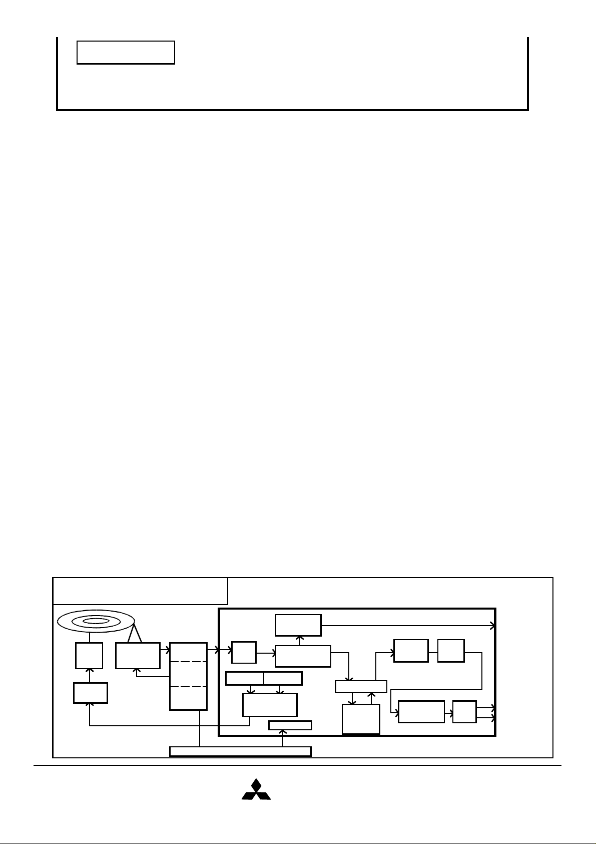
SYSTEM BLOCK DIAGRAM
M65824AFP
M
Motor
Driver
Optical
Pick-up
RF-Amp
Pick-up
Servo
Auto
Adjustment
PLL
Slicer
PLL CLK
CLV
Digital Servo
Subcode
Interface
EFM
De-modulator
OSC CLK
MCU I/F
18kSRAM
ECC
C1:2error
C2:2error
Inter
polation
4fs Digital
Filter
DeEMP
D/A
Display
L
R
System Control Microprocessor
MITSUBISHI
ELECTRIC
Page 2
MITSUBISHI SOUND PROCESSOR ICs
M65824AFP
/23
Microcomputer
CD PLAYER DIGITAL SIGNAL PROCESSOR WITH BUILT-IN DAC
1.BUILT-IN FUNCTIONS
Functional block
D/A converter
Memory
PLL
EFM demodulator
Subcode decoding
CRC decoding
Description:
• 64fs 1bit Σ∆ D/A converter
• S/N:74dB(theoretically)
• 18kSRAM(built-in)
• ±8 fames jitter margin
• Adjustment free VCO
• Slice level control
• EFM demodulation
• Frame sync.detection,protection&interpolation
• Frame sync.signal output
• Subcode P to W decoding,serial output
• Subcode Q register
• Subcode Q-CRC Check
• Subcode sync.signal output(S0/S1)
• Emphasis detection,built-in de-emphasis
circuit control
• C1:Duplex,C2:Duplex
• De-scramble
• De-interleave
• Error monitor output
Data interpolator • Averaging/Holding
D/A interface
Digital filter • 4 times over sampling digital filter
De-emphasis
CLV digital servo
interface
Digital audio
interface
HFD
• Muting control
• Digital de-emphasis (IIR type digital filter)
• Automatic emphasis flag detection
• PWM output
• Low disc rotation detection
• CLV digital servo control
• Muting control
• Attenuation(-12dB)
• Subcode Q register interface
• Digital audio interface output ON/OFF
• Clock accuracy input
• TLC voltage "hold"
• LPF output "open"
• PWM output "regular acceleration"
MITSUBISHI
ELECTRIC
2
Page 3
MITSUBISHI SOUND PROCESSOR ICs
M65824AFP
/23
2. PIN CONFIGURATION
AVSS
LOCK/DRD
TEST I/O
DOTX
XI
DVSS
TEST
SBCO
SYCLK
KILLB
HF
AVDD
IREF
EXP2
MSD
MCK
DVSS2
PWM
SCAND
CRCF
DVDD
3
CD PLAYER DIGITAL SIGNAL PROCESSOR WITH BUILT-IN DAC
ADJCLK
ACLRB
C423/DSCK
XO
1
2
3
4
5
6
7
8
9
10
11
42
41
40
39
38
37
36
35
34
33
32
RAGND
ROUT/LRCK
RAVDD
LAVDD
LOUT/DO
LAGND
EXP1
MLAB
SCCK
EFFK
EST1
EST2
TLC
LPF
12
13
14
15
16
17
18
19
20
21 22
31
30
29
28
27
26
25
24
23
DVDD2
SBQS
DSPS
MITSUBISHI
ELECTRIC
Page 4
MITSUBISHI SOUND PROCESSOR ICs
M65824AFP
/23
4
CD PLAYER DIGITAL SIGNAL PROCESSOR WITH BUILT-IN DAC
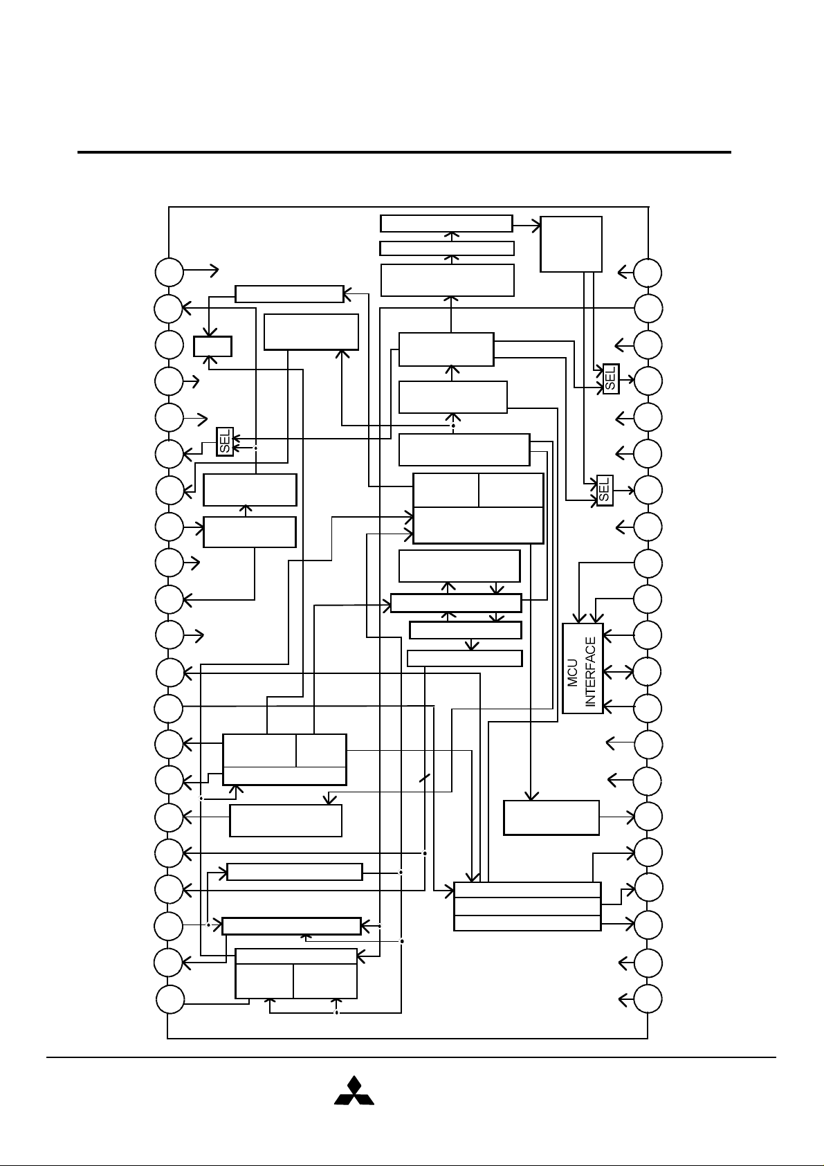
3. BLOCK DIAGRAM
AVSS
ADJCLK
LOCK/DRD
TESTI/O
ACLRB
C423/DSCK
DOTX
XI
DVSS
XO
1
2
3
4
5
6
7
8
9
10
ANALOG
GND
3/4DETECTOR
SEL
TEST
CONTROL
RESET
X'tal TIMING
GENERATOR
CLOCK
GENERATOR
DIGITAL
GND1
DIGITAL AUDIO
INTERFACE
Σ∆ MODULATOR
Dither
16fs DIGITAL
FILTER
4fs DIGITAL
FILTER
DE-EMPHASIS
FILTER
INTERPOLATION
MUTE CONTROL
FREQ
CONTROL
18K SRAM
(8bit×2400WORD
MEMORY CONTROL
PHASE
CONTROL
CLV SERVO
CONTROL
1bitD/A
LPF
L/Rch
42
AVDD
41
IREF
RAGND
40
ROUT/LRCK
39
RAVDD
38
LAVDD
37
36
LOUT/D0
35
LAGND
34
EXP2
33
EXP1
TEST
SBCO
SCCK
SYCLK
EFFK
KILLB
EST1
EST2
HF
TLC
LPF
11
12
13
14
15
16
17
18
19
20
21
TEST
CONTROL
SYNC DET.
PROTECT
EFM TIMING GEN.
DIGITAL SILENCE
DETECTOR
HFD Generate
HF COMPARATOR
VCO
FREQ
DET.
EFM
DEMOD
.
PHASE
DET.
CIRC DECODER
ERROR MONITOR
HFD CONTROL
DIGITAL
GND2
DIGITAL
VDD2
PWM
MODULATOR
SUBCODE DEMOD
SUBCODE Q CRC
SUBCODE Q REGISTER
VDD for
INTERNAL
LOGIC
DIGITAL
VDD1
32
31
30
29
28
27
26
25
24
23
22
MLAB
MSD
MCK
DVSS2
DVDD2
PWM
SCAND
CRCF
SBQS
DSPS
DVDD
MITSUBISHI
ELECTRIC
Page 5
MITSUBISHI SOUND PROCESSOR ICs
M65824AFP
/23
5
CD PLAYER DIGITAL SIGNAL PROCESSOR WITH BUILT-IN DAC
4. PIN DESCRIPTION
pin No.
Name I/O Function
1 AVSS 2 ADJCLK O
3
LOCK/DRD
4 TEST I/O I
5 ACLRB I
6
C423/DSCK
7 DOTX O
8 XI I
9 DVSS -
10 XO O
O
O
Analog system GND
Clock output for servo adjustment:f=88.2KHz
Lock monitor / low disc rotation detect
output
Test control
System reset input : reset ="L"
No pull-up
Crystal system clock output f=4.2336MHz
Ext.D/A mode: Data shift clock output
Digital out
Crystal oscillator input (with Feedback R)
f:8.4672MHz
Digital system GND
Crystal oscillator output
11 TEST I
12 SBCO O
13 SCCK I
14 SYCLK O
15 EFFK O
16 KILLB O
17 EST1 O
18 EST2 O
19 HF I
20 TLC O
21 LPF I/O
22 DVDD -
Normal/Test select input : Test"H"
Subcode serial output
Shift clock input for subcode data read
Frame lock status output : Lock="H"
EFM frame clock output : duty=50%
Digital silence : DIGITAL ZERO="L"
Opendrain output
Error status output 1
"H"When error detect at C1 decoder
Error status output 1
"H"When error detect at C2 decoder
High frequency signal input
Slice level control signal output
Loop filter for PLL
Digital interface power supply
23 DSPS -
Digital system power supply(internal logic)
MITSUBISHI
ELECTRIC
Page 6
MITSUBISHI SOUND PROCESSOR ICs
M65824AFP
/23
4.PIN DESCRIPTION(CONTINUANCE)
6
CD PLAYER DIGITAL SIGNAL PROCESSOR WITH BUILT-IN DAC
pin No.
Name I/O Function
Subcode Q register read interrupt signal
24 SBQS O
"L" for read
25 CRCF O CRC checked results of Subcode Q:CRC OK="H"
26 SCAND O Subcode sync.signal output:"H" for sync.
27 PWM O Disc motor driver PWM output(Both sides)
28 DVDD2 - Digital interface power supply2
29 DVSS2 - Digital system GND2
30 MCK I Microcomputer interface shift clock input
31 MSD I/O Microcomputer interface serial data I/O
Microcomputer interface latch clock
32 MLAB I
Built-in 22KΩ pull up resistor to DVDD
Input pin (be read via serial I/F) No.1
33 EXP1 I
Built-in 4.7KΩ pull up resistor to DVDD
34 EXP2 I
Input pin (be read via serial I/F) No.2
Built-in 4.7KΩ pull up resistor to DVDD
35 LAGND - Lch Analog GND
Audio signal output(L-ch)
36 LOUT/D0 -
Ext.D/A mode;Audio serial data output
37 LAVDD O Lch Analog power supply
38 RAVDD - Rch Analog power supply
39
ROUT/LRCK
O
Audio signal output(R-ch)
Ext.D/A mode;LR clock output
40 RAGND - Rch Analog GND
41 IREF I PLL circuit reference current setting
42 AVDD - Analog System power supply
Schmitt trigger input is the following
ACLRB(No.5),TEST(No.11),SCCK(No.13),MCK(No.30)
MLAB(No.32),EXP1(No.33),EXP2(No.34)
Reset condition for ACLRB(No.5:No pull-up resistor,Normal CMOS input)
minimum reset time :1µsec
MITSUBISHI
ELECTRIC
Page 7
MITSUBISHI SOUND PROCESSOR ICs
M65824AFP
/23
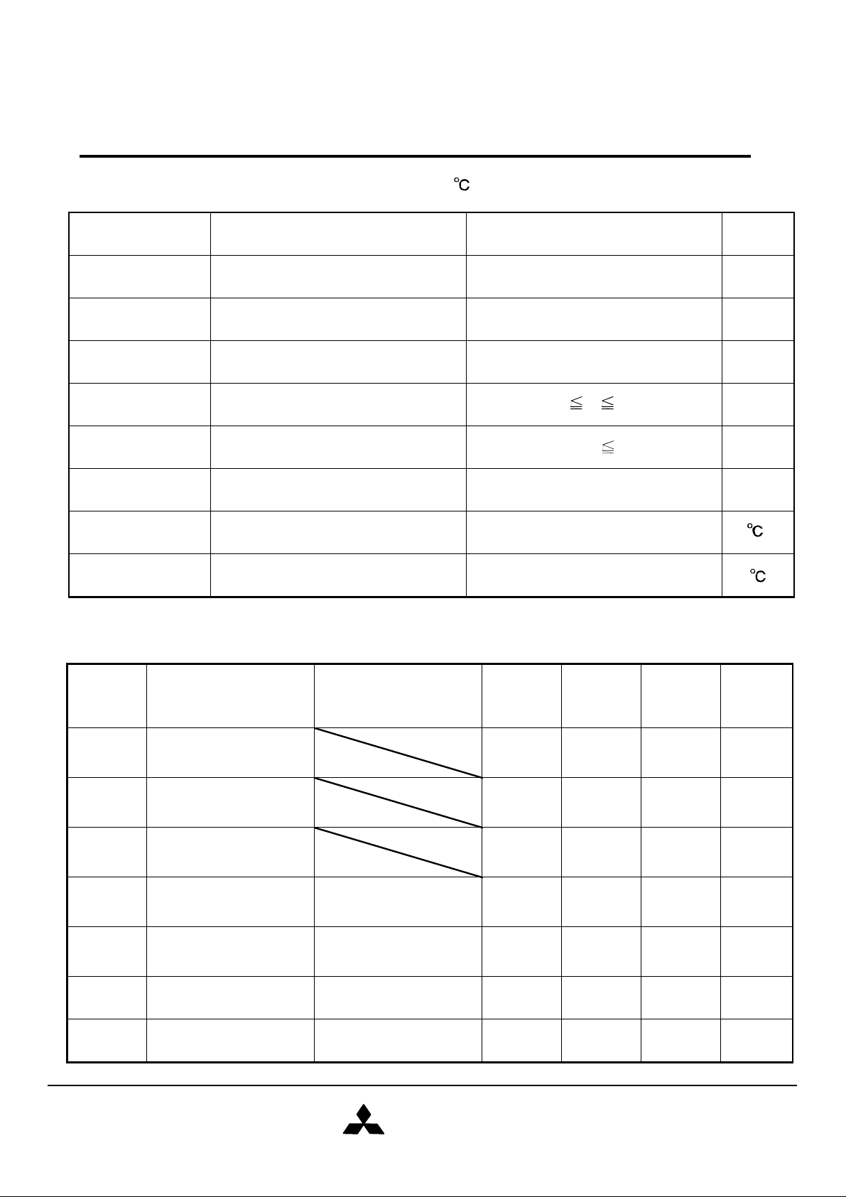
5.ABSOLUTE MAXIMUM RATINGS
(Ta=25
,unless otherwise noted)
7
×
CD PLAYER DIGITAL SIGNAL PROCESSOR WITH BUILT-IN DAC
Symbol Item Rating Unit
DVDD-DVSS Supply voltage(interface) -0.3 to +6.5 V
AVDD-AVSS Supply voltage(analog) -0.3 to +3.6 V
DSPS-DVSS Supply voltage(internal) -0.3 to +3.6 V
Vi Input voltage
DVSS-0.3 Vi DVDD+0.3
V
Vo Output voltage DVSScVo DVDD V
Pd Power dissipation 350 mV
Topr Operating temperature -10 to +70
Tstg Storage temperature -40 to +125
6.RECOMMENDED OPERATING CONDITIONS
Symbol Item conditions Min Typ Max Unit
DVDD
AVDD
Supply voltage
(interface)
Supply voltage
(analog)
2.7 5.0 5.5 V
2.7 3.0 3.3 V
Supply voltage
DSPS
VIH
VIL
(internal)
Input voltage
("H"level)
Input voltage
("L"level)
Output frequency Normal speed
fosc
fvco
Output frequency Normal speed
Except
Schmitt input
Except
Schmitt input
MITSUBISHI
ELECTRIC
2.7 3.0 3.3 V
DVDD 0.7
DVSS -
- 8.4672 - MHz
- 8.4636 - MHz
- DVDD V
×
DVDD 0.3
V
Page 8

MITSUBISHI SOUND PROCESSOR ICs
M65824AFP
/23
7.ELECTRICAL CHARACTERISTICS
(Ta=25
,DVDD=5V,AVDD/DSPS=3V unless otherwise noted)
(Ta=25
,DVDD=5V,AVDD/DSPS=3V unless otherwise noted)
VIH=4.5V
VIL=0.5V
8
Ioh=-4.0mA
Iol=4.0mA
CD PLAYER DIGITAL SIGNAL PROCESSOR WITH BUILT-IN DAC
Symbol Item conditions Min Typ Max Unit
IDD
Circuit current
VOH 4.5 - - V
VOL - - 0.4 V
IIH - - 2
IIL -2 - -
Output voltage
("H"level)
Output voltage
("L"level)
Input current
("H"level)
Input current
("L"level)
Pull up resistor
Ru
fosc=8.4672MHz
fvco=8.6436MHz
DVDD=5.0V
IOH=-1.0mA
DVDD=5.0V
IOL=1.0mA
EXP1(33),EXP2(34)
MLAB(32)
- 20.0 - mA
2.35
11
-
-
9.4
44
VOH output voltage DVDD=5.0V
(DOTX)
("H"level)
4.6 - - V
VOL output voltage DVDD=5.0V
(DOTX)
("L"level)
- - 0.4 V
Ileak output
(DOTX)
Tf output
Tr output
leakage current
(DOTX)
fall time
(DOTX)
rise time
DVDD=5V - - 10
CL=20pF - - 10 nsec
CL=20pF - - 10 nsec
µΑ
µΑ
ΚΩ
µΑ
8.D/A converter output
Symbol Item conditions Min Typ Max Unit
Maximum output
Vomax 1.8 2.0 2.2 V
Freq - -3.0 - dB
voltage
Frequency
characteristic
THD Distortion
Signal noise
SNR
DR
ratio
Dynamic range
Vgpass Passband ripple
with System
construction
with System
construction
20Hz to 20KHz
(20KHz LPF)
20KHz LPF
A-weighted(20KHz LPF)
at-60dB(20KHz LPF)
(at 20KHz)
at 20KHz
MITSUBISHI
ELECTRIC
- - 0.2 %
72
72 - - dB
- -
dB
72 - - dB
- - -1.5 dB
Page 9

MITSUBISHI SOUND PROCESSOR ICs
M65824AFP
/23
9. POWER SUPPLY
9
M65824AFP
M65824AFP
CD PLAYER DIGITAL SIGNAL PROCESSOR WITH BUILT-IN DAC
2.7 to 3.3V
1 AVSS
9 DVSS
29 DVSS2
35 LAGND
40 RAGND
Fig.1 Application for 3.0V system
Fig.1 shows an application circuit for 3.0V system.
Voltage range is between 2.7V to 3.3V.
Fig.2 shows an application circuit for 5.0V system.
The M65824AFP needs dual power supply.
AVSS,DVSS,DVSS2,LAGND and RAGND should be connected to GND(0V).
DVDD2 28
DVDD 22
DSPS 23
LAVDD 37
RAVDD 38
AVDD 42
1 AVSS
9 DVSS
29 DVSS2
35 LAGND
40 RAGND
Fig.2 Application for 5.0V system
DVDD2 28
DVDD 22
DSPS 23
LAVDD 37
RAVDD 38
AVDD 42
3.6 to 5.5V
2.7 to 3.3V
(Fig.1 and Fig.2)
10. FUNCTION DESCRIPTION
10-1 MICROCOMPUTER INTERFACE
(1) Connection
M65824AFP
MSD
31
CD-DA
SIGNAL
PROCESSOR
(2) Pin description
MLAB:Microcomputer latch line for latching commands into the
M65824AFP and for switching the communication mode.
(MLAB=1:µP writes to the M65824AFP)
(MLAB=0:µP reads from the M65824AFP)
30
32
MCK
MLAB
I/O
O
O
µP
MITSUBISHI
ELECTRIC
Page 10

MITSUBISHI SOUND PROCESSOR ICs
M65824AFP
/23
10
CD PLAYER DIGITAL SIGNAL PROCESSOR WITH BUILT-IN DAC
MCK:Microcomputer clock line for clocking bits to or from the
M65824AFP.
MSD:Microcomputer data line for sending or receiving data bits from
the M65824AFP.
(3) Operation
*Microcomputer command read/write operation
The data bits (MSD) are accepted on the rising edge of the clock
pulse(MCK).The falling edge of the latch line(MLAB) decides the
complete command.
At the same moment the data line is switched to output mode and
indicates the status as requested by data bits D3,D2,D1 and D0.
When the latch line becomes high,the data line is switched to
input mode.
*Status request / interface command
If the microcomputer wants to read a certain status, it has to
write a status request command with the appropriate bits D3,D2,D1
and D0 to the M65824AFP. After latching the command into the
M65824AFP, the data line becomes the request status information
as long as the latch line(MLAB) remains low.
(4) Microcomputer I/O timing
MSD
D0 D1 D2 D3 D4 D5 D6 D7
Status
MCK
t1
t3
t2
t4
MLAB
t5
t1:Shift clock width (min.200nsec)
t2:Shift clock setup time (min.100nsec)
t3:Shift clock hold time (min.100nsec)
t4.Latch pulse setup time (min.100nsec)
t5:Latch pulse width 50nsec t5 50µs
Subcode-Q reading:50nsec t5
MITSUBISHI
ELECTRIC
Page 11

MITSUBISHI SOUND PROCESSOR ICs
M65824AFP
/23
Disc motor mode
Audio function
Status Request/Interface command
D7D6Function
0
0
0
1
Disc motor accelerate,applies maximum voltage for acceleration to the disc mo
1
0
1
1
D5D4Function
0
0
0
1
1
0
1
1
D3D2D1D0Function
000
1
PLL lock status,Status="L" when PLL is locked
001
0
Subcode ready status,Status="L" when new subcode has been receive
001
1
Status=Logical value of EXP1(Pin33)
010
0
Status=Logical value of EXP1(Pin34)
010
1
011
0
011
1
111
1
11
Internal D/A mode , DOTX : OFF , Disc motor switched off , Audio muted , ACCK c
CD PLAYER DIGITAL SIGNAL PROCESSOR WITH BUILT-IN DAC
(5) M65824AFP commands table
Initial value after power on:00000000
D7 D6 D5
(6) Data description
Reset condition
function
Disc motor Mode
Audio function
lock level :
D4
D3 D2 D1
D0
Disc motor switched off
Disc motor brake,applies maximum voltage for braking to the disc motor
Disc motor CLV control mode
Audio muted
Audio mute off
Prohibited
Audio attenuate by 12dB
Status request / Interface command
Disc rotation down status,Status="L" when disc motor speed <2/3
0 0 0 0
of nominal speed
DOTX output
DOTX off (high impedance)
ACCK Clock accuracy input Level
1 0 0 0
ACCK Clock accuracy input Level
1 0 0 1 External D/A mode (IIS)
1 0 1 0 External D/A mode (EIAJ)
Internal D/A mode
MITSUBISHI
ELECTRIC
Page 12

MITSUBISHI SOUND PROCESSOR ICs
M65824AFP
/23
12
CD PLAYER DIGITAL SIGNAL PROCESSOR WITH BUILT-IN DAC
(7) Subcode Q register interface
The data of subcode Q stored in the internal 80-bit register can
be read with a serial clock from the microcomputer.
Procedure
1. THE microcomputer has to issue a subcode ready status command
to the M65824AFP.
Set MSD data "0100xxxx" and write to the M65824AFP.
2. If the status returned by the M65824AFP equals to subcode ready
(status="L") then the microcomputer can read a subcode-Q data.
3. If the status is ready then the microcomputer starts clocking
out the subcode-Q data from the M65824AFP with remaining the
latch line "MLAB" status "L" as long as the microcomputer
requires.
4. The microcomputer certainly sends 81 clocks.
From the first clock to 80th clock read out subcode-Q data and
81th clock sets the status "H".
5. When the microcomputer finishes reading the subcode-Q data,
(send 81 clocks) "MLAB" should be changed from "L" to "H".
6. If communication is aborted or doesn't finish normally,the
M65824AFP and sends 81 clocks for initializing the internal 80-bit
register and setting status "H".
typ.136µsec
SBQS
MSD
B1 B2 B3 B4 B5 B6 B7 B8 B9 BA
typ.13.3msec
MSD
MCK
MLAB
StatusDon't care
t6
Q7
Q8
MITSUBISHI
ELECTRIC
Q6
Q5
Q4
Q3
Q2 Q1 15 14 13
t6:Mode setup time(min.400nsec)
Page 13

MITSUBISHI SOUND PROCESSOR ICs
M65824AFP
/23
13
CD PLAYER DIGITAL SIGNAL PROCESSOR WITH BUILT-IN DAC
Description
Conditions under which the SBQS is placed in "L"
(a) When the CRC checked results is good.
(b) When both subcode sync signals S0 and S1 are detected in the
specified position
When both conditions (a) and (b) above are satisfied, the SBQS pin
outputs "L".
If SBQS does not turn to "L" then the subcode ready status indicates
"H" (=not ready).When the subcode ready status is "H",the
microcomputer can not read a valid subcode Q-channel data from
the M65824AFP.
The subcode-Q data is renewed at the same timing of the signal
"SBQS" status is "L".
When the microcomputer send a subcode ready status command,if
the signal "MLAB" is changed from "H" to "L" during the signal
"SBQS" status is "L" then the M65824AFP will return the status
not ready. (status="H")
While the latch line "MLAB" is remained "L", the subcode-Q data
is not renewed.
The M65824AFP output a subcode-Q data with reversed each 1-byte.
(8)Subcode interface R-W
The subcode data(P,Q,R,S,T,U,V,W) can be read from the SBCO pin
by inputting clocks to the SCCK pin among the data converted from
14-bit EFM signal to 8-bit symbol.
When both subcode sync. patterns S0,S1 are detected in the
specified position as a sync. signal of this subcode, a sync.
signal is output from SCAND pin.
If 8 or more clocks are input to the SCCK, the SBCO is placed in "L".
10-2 DISCMOTORCONTROLPULSE(CLVMODE)
PWM
(BOTH SIDES)
(ACCELERATION)
22.6757µ sec
Min:0.2362µ sec
Max:15.117µ sec
MITSUBISHI
ELECTRIC
(DECELERATION)
Hi-Z
Min:0.2362µ sec
Max:15.117µ sec
22.6757µ sec
Page 14

MITSUBISHI SOUND PROCESSOR ICs
M65824AFP
/23
14
TLC
LPF
VCO
HFD
IREF
HF comparator
1/2
VCO
Timer
TLC
LPF
Vref
CD PLAYER DIGITAL SIGNAL PROCESSOR WITH BUILT-IN DAC
10-4. EFM - PLL circuit
(1) Data slicing / PLL
The M65824AFP has an analog front -end for incoming HF (EFM) signal. Using CMOS - Analog
technology , the front - end is comprised of an automatic slice level control circuit and EFM - PLL
circuit with internal adjust - free VCO. Under figure shows a block - diagram of the analog front - end.
The HF signal is sliced by the HF comparator and a DC level is feed back from TLC to HF through some
the external CR. If HFD becomes "H" because of defect in disk, then TLC becomes off state and holds
the DC level. EFM -PLL is for extracting the EFM clock signal from the HF signal. The PLL circuit has a
phase / frequency comparator so the M65824AFP has a wide capture / lock range and there is no need
to adjust the VCO. LPF is the charge- pump output and same - time control voltage input to the VCO.
LPF becomes off state if HFD becomes "H".
IREF is the reference current input used to determine the current of charge pumps of TLC and LPF,
operating point of HF comparator , and VCO free running frequency.
If IREF is connected to a noisy power supply through a resistor , the VCO would be modulated and the
error - rate would increase. Therefore , power supply noise at IREF must be held to a minimum.
HF
signal
HF comparator
Current
source
control
changepump
EFM
Data
phase
Det.
to EFM
demodulator
EFM
Clock
changepump
Freq.
Det
changepump
Low freq
limiter
Async frame
counter
MITSUBISHI
ELECTRIC
Sync protection
block
Page 15

CD PLAYER DIGITAL SIGNAL PROCESSOR WITH BUILT-IN DAC
M65824AFP
/23
15
(2) Automatic slice level control
CHF
HF signal
RTLC
CTLC
(3) PLL circuit
RLPF
CLPF
RPD
CLPF
C1
C1
(4) Reference current
HF
M65824AFP
TLC
LPF
M65824AFP
HF
M65824AFP
IREF
MITSUBISHI SOUND PROCESSOR ICs
The slice level control circuit is formed by
connecting a resistor and capacitors to the
HF (High - frequency signal input ) pins.
TLC(Slice level control output) pins.
(Tentative Value)
CHF=0.0010µ F
CTLC=0.022µ F
RTLC=33KΩ
Vin HF 0.5Vp-p min
Since the adjustment - free VCO is built in,
the adjustment - free PLL circuit can be
formed by connecting a resistor and
capacitors to the LPF (Low - pass filter)
pin.
(Tentative Value)
CLPF=470pF
C1=0.15µ F to 1.0µF*
RLPF=1.8KΩ
RPD=3.3MΩ
From 0.15µ F to 1.0µF capacitor is
available for C1.
In high speed search such as track count
search,the rotation of disc decrease. If this
is problem, this problem is improved by
using large C1.
A resistor must be connected between the
IREF pin and VDD in order to set the
reference current used in determining the
current values of the TLC pin and LPF
pin , the comparator operating current
of the slice level control circuit , and the
VCO free - run frequency.
(Tentative Value)
RIREF=100KΩ(Normal speed)
MITSUBISHI
ELECTRIC
Page 16

MITSUBISHI SOUND PROCESSOR ICs
M65824AFP
/23
23bit S/R
1/2
EFM timing generator
SYCLK
PLL control
Timer
EFM Symbol
VCO
HFD
16
CD PLAYER DIGITAL SIGNAL PROCESSOR WITH BUILT-IN DAC
10-5.EFM demodulation
The EFM signal that has been converted to logic level , and the EFM clock that has been extracted from
the EFM signal are input to the demodulator and convert to 8bit symbol.
The EFM demodulation depend on EFM table in the RED book.
To demodulate , the demodulator must be synchronized to EFM signal for each frame. The frame
sync.protection circuit holds the synchronization inspire of some lack of sync.pattern, and prevents false
synchronization of the demodulator bit - slipping or mis - synchronization occurs.
Frame sync.control block diagram show Fig.3.
Edge
dat.
÷17
÷35
Sync det.
Sync
÷588
Tfs
Sync.
control
Sync.frame
counter
Window
Reset
Window
generation
Lock state
det.
Fig.3Frame sync.control block diagram
The generating condition of counter reset signal (Reset ) in the EFM timing generator is indicated as
follows
Reset = (Sync * Tfs ) + (Sync * Window)
*:Logical product
+:Logical sun
Sync:Synchronizing signal
Tfs:Detection signal of synchronizing signal
space = 588
Window:Window signal ±7ck
In the synchronous state , Sync and Tfs generate simultaneously and Sync comes to the center of the
window. At this time , "H" is output to the SYCLK pin , and EFM signal is synchronized by frame unit.
Content
Frame lock
Frame unlock
SYCLK
L
H
MITSUBISHI
ELECTRIC
Page 17

MITSUBISHI SOUND PROCESSOR ICs
M65824AFP
/23
17
To monitor a sync.state with a control microcomputer,it is necessary to provide a signal from
In M65824AFP, this signal is allocated to LOCK/DRD pins.When the braking instruction from
Not BRAKE
CD PLAYER DIGITAL SIGNAL PROCESSOR WITH BUILT-IN DAC
which a short-period missing of sync.pattern due to a disc defect,which occurs even in a
sync.state is eliminated.
the microcomputer is not input, the LOCK/DRD pins monitor the sync.state in 1/16period of
EFM frame clock, outputting the results; if monitored status is "locked" then output is "H" ,
continuous 8 times "unlocked " output becomes "L".
And , when the disc rotation does not become the target speed , lock monitor may become
"LOCK" state. In such state , some internal circuit does not work. So when the disc rotation
become the target speed and change from rough servo mode to CLV mode , LOCK / DRD
output lock monitor.
LOCK/DRD pin outputs DRD signal when the disc motor is braking under the command
from MCU.
Condition
status
BRAKE status
Content LOCK/DRD
Unlock by 1/16 frame clock
Lock by 1/16 frame clock
(Not CLV mode)
Lock by 1/16 frame clock
( CLV mode)
Low disc rotation monitor signal
L
H
DRD signal
MITSUBISHI
ELECTRIC
Page 18

MITSUBISHI SOUND PROCESSOR ICs
M65824AFP
/23
CD PLAYER DIGITAL SIGNAL PROCESSOR WITH BUILT-IN DAC
10-6 Low disc rotary control
When M65824AFP detects than the number of rotations is less than 2/3 that of the normal
play state and the disc motor is braking under the command from MCU, it outputs the disc
rotation deterioration signal to LOCK / DRD pin.
LOCK monitor
LOCK/DRD
BRAKE
Term
Not BRAKE
BRAKE
DRD
Content
Sync.status monitor output
Disc rotation speed is more than 2/3
Disc rotation speed is less than 2/3
Less than 2/3 frequency
LOCK/DRD
LOCK
L
H
MITSUBISHI
ELECTRIC
18
Page 19

CD PLAYER DIGITAL SIGNAL PROCESSOR WITH BUILT-IN DAC
M65824AFP
/23
19
SHIFT REGISTER
AUX
SUB frame format
Frame format
Channel coding(Biphase mark modulation)
10-7. DIGITAL OUT
The digital audio signal formatted according to EIAJ
Standard CP-340 "Digital Audio Interface" is
outputted to DOTX pin.
The validity flag is internally set to "1" automatically
when the interpolated word is transmitted.
The user data, which is read in the subcode
interface
circuit,is transmitted.
Channel clock precision can be set from the outside
so that it is compatible with the validity pitch.
The channel status is set to level in the validity
pitch,mode,and level is set automatically when it
is not in the validity pitch mode.
B:CHANNEL L AND TOP OF BLOCK
M:CHANNEL L EXCEPT TOP OF BLOCK
{
W:CHANNEL R
MITSUBISHI SOUND PROCESSOR ICs
AUDIO DATA
Clock
Accuracy
CHANNEL
STATUS
CONTROL
CHANNEL STATUS
VALIDITY FLAG
SHIFT REGISTER
SHIFT REGISTER
PARITY BIT
USER DATA
16
C U V
EST2
7
SUBCODE Q TO W
GENERATION OF
PREAMBLE
BIPHASE MARK
MODULATION
PARITY
GENERATI
ON
TIMING
CIRCUIT
DOTX
SYNC
4 BIT 4 BIT 4 BIT LSB 16 BIT MSB
M
L CHANNEL
SOURCE CODING
If Digital-OUT is not used to prevent spurious radiation, it
is possible to turn DOTX pin output "OFF" by setting mode
command of microcomputer interface.
Channel status clock precision can be set by ACCK command
of microcomputer interface.
W R CHANNEL B L CHANNEL W R CHANNEL M L CHANNEL
AUDIO DATAEXTENDED BIT
SUB FRAMESUB FRAME
V U C P
1 1 1 1
FRAME 1FRAME 0FRAME 191
MITSUBISHI
ELECTRIC
Page 20

MITSUBISHI SOUND PROCESSOR ICs
M65824AFP
/23
10-8.HFD
20
Fig.4 TLC voltage hold unit block diagram.
CD PLAYER DIGITAL SIGNAL PROCESSOR WITH BUILT-IN DAC
HFD is high frequency signal missing detect circuit.
HFD is "ON" at HF signal missing.
1) TLC voltage "hold"
2) LPF output "open"
3) PWM output "regular acceleration"
TLC voltage hold unit
The block diagram for this TLC voltage hold unit is shown in Fig.4 below.
This unit holds TLC voltage in stable condition and gives this voltage at HF signal
missing.
This unit holds two kinds of TLC voltage. By this method, this unit does not hold
HF
Vref
C423
TLC voltage at HF signal missing and this unit can follow a difference of TLC
voltage with the Disc.
Edge trigger
circuit
HFD ON
counter
HFD OFF
counter
TLC HOLD
OFF counter
TLC HOLD
control
HFD
control
circuit
TLC HOLD
circuit
HFD
internal
logic
TLC
MITSUBISHI
ELECTRIC
Page 21

MITSUBISHI SOUND PROCESSOR ICs
M65824AFP
/23
8.4672MHz
21
CD PLAYER DIGITAL SIGNAL PROCESSOR WITH BUILT-IN DAC
10-9. Oscillation circuit
(1)Internal oscillation mode
The oscillation circuit can be formed by connecting a crystal
oscillator(8.4672MHz)and load capacitors to pins XI and XO.
M65824AFP
XI XO
C1 C2
Oscillator
load capacitor value(Reference)
30pF
MITSUBISHI
ELECTRIC
Page 22

MITSUBISHI SOUND PROCESSOR ICs
M65824AFP
/23
22
CD PLAYER DIGITAL SIGNAL PROCESSOR WITH BUILT-IN DAC
MITSUBISHI
ELECTRIC
Page 23

MITSUBISHI SOUND PROCESSOR ICs
M65824AFP
/23
CD PLAYER DIGITAL SIGNAL PROCESSOR WITH BUILT-IN DAC
11. System construction
0.1u
AVSS
DVSS
8.4672MHz
DVSS
SUBCODE I/F
30p
30p
1
2
3
4
5
6
7
8
9
10
11
12
13
14
15
AVSS
ADJCLK
LOCK/DRD
TEST I/O
ACLRB
C423/DSCK
DOTX
XI
DVSS
XO
TEST
SBCO
SCCK
SYCLK
EFFK
AVDD
IREF
RAGND
ROUT/LRCK
RAVDD
LAVDD
LOUT/D0
LAGND
EXP2
EXP1
MLAB
MSD
MCK
DVSS2
DVDD2
42
41
40
39
38
37
36
35
34
33
32
31
30
29
28
100K
Audio
R-CH
Audio
L-CH
0.1u
AVSS
Microcomputer
I/F
100p
HF INPUT
0.15u
470p
33K
2200p
0.01u
1.8K
16
17
18
19
20
21
KILLB
EST1
EST2
HF
TLC
LPF
PWM
SCAND
CRCF
SBQS
DSPS
DVDD
MITSUBISHI
ELECTRIC
27
26
25
24
23
22
Motor
Driver
AVSS
DVSS
DVDD
DSPS
AVDD
23
 Loading...