

Page 1
MITSUBISHI ICs (TV)
PRELIMINARY
Notice:This is not a final specification.
Some parametric limits are subject to change.
DESCRIPTION
The M65675FP/M65676FP is a NTSC/PAL encoder LSI that
converts CCIR 601 or CCIR 656 (SMPTE125M) format digital video
signals into analog component and composite video signals in
accordance with either NTSC or B/G-PAL standards.
The 10-bit digital luma (Y) and analog chroma (U/V) signals are
available in Y/U/V output mode.
In addition it performs the closed caption capability (TV line 21/
NTSC), CGMS
line 23/PAL), Macrovision copy protection
*1
encoding (TV line 20/NTSC), WSS
*3
function (Rev. 7.01) and
on-screen display. The OSD function can be directly accessed by
the OSD microprocessor via built-in interface.
FEATURES
•
NTSC and B/G-PAL Outputs
•
Component Y/C (S-Video), Composite (CVBS) or Y
Outputs
•
Supporting CCIR601, CCIR656 (SMPTE125M) Format Data
•
Processing Y/Cb/Cr and Y/U/V Pixel Data
•
27MHz Clock Frequency (Two-times Oversampling)
•
Macrovision Copy Protection
•
Close Captioning Supporting (line 21/NTSC) (ODD Parity Operation)
•
V-Code Supporting (line 21/NTSC) (ODD Parity Operation)
•
•
•
*1
CGMS
Data Insertion (line 20/NTSC) (CRCC Error Correction
Code Operation)
*2
WSS
Supporting (line23/PAL)
OSD Insertion Interface and 3¥8¥4-bit Color Look-up Table
*3
Processing (Revision 7.01)
*2
encoding (TV
*4
/U/V
M65675FP/M65676FP
DIGITAL NTSC/PAL ENCODER
•
Controllable Picture Processing Functions
Color, TINT and Brightness
•
Built-in Analog Functions
Y/C Mixing
Two 10-bit DACs
Three 6-dB Amplifiers
Built-in 27 MHz System Clock Generator
•
Single 3.3V Supply
•
64-pin PQFP Package
•
Note
*1: Copy Generation Management System-A (IEC1880)
*2: Wide Screen Signaling (ETS300 294)
*3: This applies to M65675FP only.
This device is protected by U.S. patent number 4631603,
4577216 and 4819098 and other intellectual property rights.
The use of Macrovision's copy protection technology in the
device must be authorized by Macrovision and is intend for
home and other limited pay-par-view use only, unless otherwise
authorized in writing by Macrovision. Reverse engineering or
disassembly is prohibited.
*4: Y output is 10bit digital signal.
APPLICATION
DVD Players, Digital Satellite & Cable System (Set Top Boxes/
IRDs), Video CD, Multimedia Terminals, Video Games, Digital VCR
& Camcoder etc.
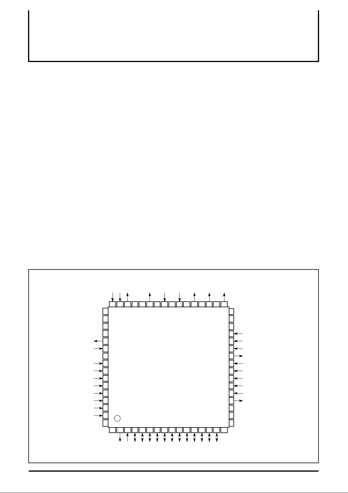
PIN CONFIGURATION (TOP VIEW)
Yref
47
48
Ycomp
49
50
N.C.
51
DV
DD1
DVSS1
52
DVSS2
DV
DD2
53
54
55
56
57
58
59
60
61
62
63
64
2
1
SS2
DV
X out
X in
PXD7
PXD6
PXD5
PXD4
PXD3
PXD2
PXD1
PXD0
Cref
DAY
46
3
PXCLK
DVASEL
SS1
AV
AVDD1
454443
5
4
VD
HD
DAC
C in
Ccomp
N.C
41
403938
42
M65675FP
M65676FP
8
7
VD8
VD7
9
VD6
6
VD9
Outline 64P6N-A
Y in
DD2
AV
101112
VD5
VD4
Y
37
VD3
CVBS
SS2
AV
363534
131415
VD2
VD1
N.C.
VD0
33
16
C
SS2
DV
32
31
30
29
28
27
26
25
24
23
22
21
20
19
18
17
N.C.
N.C.
DV
DD1
TEST
SCL
SDA
ACK
RESET
Master/slave
OSD2
OSD1
OSD0
OSDCK
DV
SS1
DVDD1
DVDD2
NC : NO CONNECTION
1
Page 2
MITSUBISHI ICs (TV)
PRELIMINARY
Notice:This is not a final specification.
Some parametric limits are subject to change.
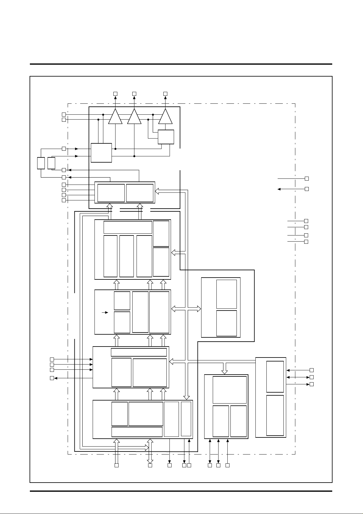
BLOCK DIAGRAM
AVSS2
AVDD2
Yin
Cin
LPF
BPF
DAC
DAY
AVSS1
AVDD1
Y ref
C ref
&
Clamp
bias
DAC
10bit
Interpolation
Y
6dB
Y/U
filter
C
6dB
10bit
DAC
C/V
6dB
MIX
Y/C
Chroma
Encoder
CVBS
Analog
M65675FP/M65676FP
DIGITAL NTSC/PAL ENCODER
TEST
RESET
DVSS2(X2)
DVSS1(X2)
DD2(X2)
DV
DD1(X2)
DV
OSD2
OSD1
OSD0
OSDCK
Encoder
Closed Caption
Y/U/V
Y/Cb/Cr
Video signal generator
OSD
Interface
Input
Interface
Manager
CGMS/WSS
Y
adder
C-sync
Burst
adder
Y
OSD
controller
Y
control
Blanking
Demulti Plexer
Manager
Video Anti Copy
signal adder (1)
Video Anti Copy
OSD mixer
Cb/Cr
Interpolation
filter
signal adder (2)
generator
sub carrier
U
V
Converter
Converter
Cb/Cr to U/V
Cb/U
Cr/V
8-color
Look-up
table RAM
Cb/U
Cr/V
CLK
generator
Oscillator
∗1
signal
generator
Anti Copy
Processing
control
register
pulse
Timing
Sync Processing
HD/VD
generator
generator
C-sync
generator
∗1: This function bloc is M65675FP only
SCL
slave
receiver
serial interface
register
Commands
SDA
ACK
Y
PXD [7:0]
VD [9:0]
PXCLK
Xout
Xin
HD
VD
/Slave
Muster
2
Page 3
± 15 µ
MITSUBISHI ICs (TV)
PRELIMINARY
Notice:This is not a final specification.
Some parametric limits are subject to change.
M65675FP/M65676FP
DIGITAL NTSC/PAL ENCODER
ABSOLUTE MAXIMUM RATINGS
Symbol Parameter
V
DD
V
I
V
O
T
a
T
stg
RECOMMENDED OPERATING CONDITION
DC supply voltage -0.3 4.5 V
Digital input voltage -0.3
Digital output voltage -0.3
Operating temperature -20 +25 +75 ° C
Storage temperature -40 +125 ° C
(Ta=25 ∞ C, DV
Symbol Parameter Test conditions
Supply
DDX
DV
AV
DI
AI
DDX
DD
DD
Digital supply voltage 3.0 3.3 3.6 V
Analog supply voltage 3.15 3.3 3.45 V
Digital current consumption 0 45 mA
Analog current consumption 0 55 mA
Digital input
IL
V
IH
V
IL
I
I
C
Input voltage
Input leakage current DV
Input capacitance f=1MHz, V
DV
DV
Digital output
OL
V
OH
V
O
C
2
I
C bus
I
O
I
OZ
Output voltage DV
Output capacitance f=1MHz, V
Output current DV
Output leakage current (off) DV
D/A converter
Res Resolution 10 Bit
INL Integral non-linearity error Rref=2.2k Ω , R
DNL Differential non-linearity error Rref=2.2k Ω , R
Vf
SMAX
Maximum output amplitude 000 to 3FF 1.5 V
6-dB amplifier
R
G
G
DR
DR
bias
V_YC
V_CV
in
out
Bias resistor 7.5 10 11.5 k Ω
Voltage gain (Y/C) 5.50 6.00 6.50 dB
Voltage gain (CVBS) 5.10 6.00 6.85 dB
Input dynamic range 0.8 V
Output dynamic range 1.6 V
Limits
Min. Typ. Max.
DD
V
V
DD
DD
=AV
+0.3
+0.3
DD
=3.3V, DV
Unit
V
V
SS
=AV
SS
=0V, unless otherwise noted)
Limits
Min. Typ. Max.
DD
=3.0V 0 0.8 V
DD
=3.6V 2.5 3.6 V
DD
DD
DD
DD
I
=3.0V , V
=0V or V
DD
=0V 7 15 pF
=3.3V, | IO | <1 µ A
DD
=0V 7 15 pF
=3.0V , V
IL
=3.6V , V
=0V or V
I
L
L
I
=3.6V
3.25 V
=0.4V 4.0 mA
=3.6V
I
=300 Ω±
=300 Ω±
0.05 V
± 15 µ A
2.0 LSB
1.0 LSB
Unit
A
P-P
P-P
P-P
3
Page 4

MITSUBISHI ICs (TV)
◊
◊
◊
PRELIMINARY
Notice:This is not a final specification.
Some parametric limits are subject to change.
M65675FP/M65676FP System Architecture
Block Diagram of M65675FP/M65676FP
The M65675FP/M65676FP block diagram is shown in Fig. 3.1.
The M65675FP/M65676FP consists of 4 functional blocks: a video
signal processing, a synchronization control, a serial interface and
an analog signal processing blocks. The video signal processing
block includes an input interface, OSD interface, YCbCr to YUV
converter/encoder and copy protection signal generator (This
function block is M65675FP only).
A sync generator and timing pulse generator are in the
synchronization control block. The serial interface block has an I
slave register and command register. The analog signal processing
block includes two 10-bit DACs, a Y/C mixing circuit and three 6-dB
amplifiers.
General Description of Each Functional Blocks
Video Signal Processing Block
The Y/Cb/Cr or Y/U/V are converted into digital Y/C signals in
accordance with either NTSC and B/G-PAL standards. In addition
the closed caption, CGMS/WSS and copy protection signals will be
inserted in that digital Y/C signals.
[Input Interface]
The multiplexed Y/Cb/Cr or Y/U/V pixel data are divided by the
individual components, then the Cb/Cr or U/V data rate is increased
from 6.75 Mbps up to 13.5Mbps.
[OSD Interface]
The digital video signal in the CLT (Color Look-up Table) is overlaid
with OSD data according to the external instructions.
[Y/Cb/Cr to Y/U/V Converter]
It converts the Y/Cb/Cr into Y/U/V, and then c-sync and burst signals
are inserted on the converted Y and U/V signals, respectively.
However, the burst insertion is not done in the Y/U/V output mode.
[Encoder]
The closed caption, CGMS/WSS and copy protection signals are
inserted into the Y signal and C signal is modulated into the
appropriate standards. After that processing, both Y and C signals
will be oversampled.
[Copy Protection Processing]
According to the copy protection setting, VBI pulse (AGC and
backporch pulse) and Advanced Split Burst are generated in
accordance with Macrovision Rev 7.01.
2
M65675FP/M65676FP
DIGITAL NTSC/PAL ENCODER
Synchronization Control Block
C-sync and several timing control signals for internal use are
generated with 3 different H/V sync signals as reference. 1st
reference H/V sync signal is external input, 2nd is internally
generated one and 3rd is decoded one in digital blanking code
(SAV, EAV etc.)
Serial Interface Block
The registers can be read and written according to I
The data transport to the internal blocks is performed on the trailing
edge of V-sync, except for some set-up registers.
C
◊ Analog Signal Processing Block
The output of the 10-bit DAC is 1.2VP-P at the sampling frequency
of 27.0MHz. The inputs of Yin and Cin are set up to 0.6VP-P (Typ)
and the component outputs will be amplified by 6-dB up to 1.2VP-P
(Typ). The analog composite signal from the mixing circuit is also
amplified up to 1.2VP-P (Typ)
Functional Description
Video Signal processing
Input Interface
Input Format
The video encoder accepts 16/8-bit CCIR601 and CCIR656 format.
The specifications of these format are described as follows;
◊ 16-bit CCIR601 Interface
PXCLK=13.5MHz
Y=8-bit/13.5Mbps
16-235 straight-binary-data
Cb/Cr=8-bit/13.5 Mbps (Cb=Cr=8-bit/6.75 Mbps)
16-240 128 offset-binary-data
Active video area525/60=720-pixel¥480 line/frame
(22/284 line-263/525 line)
625/50=720-pixel¥576 line/frame
(23/336 line-310/623 line)
◊ 8-bit CCIR601 Interface
PXCLK=27.0MHz
Cb/Y/Cr=8-bit/27.0Mbps
Y= 8-bit/13.5Mbps
16-235 straight-binary-data
Cb/Cr=8-bit/13.5Mbps (Cb=Cr=8-bit/6.75Mbps)
16-240 128 offset-binary-data
Active video area525/60=720-pixel¥480 line/frame
(22/284 line-263/525 line)
625/50=720-pixel¥576 line/frame
(23/336 line-310/623 line)
2
C bus format.
4
Page 5

MITSUBISHI ICs (TV)
PRELIMINARY
Notice:This is not a final specification.
Some parametric limits are subject to change.
◊ CCIR656 Interface
PXCLK=27.0MHz
Cb/Y/Cr=8-bit/27.0Mbps
Y=8-bit/27.0Mbps
16-235 straight-binary-data
Cb/Cr=8-bit/13.5Mbps (Cb=Cr=8-bit/6.75 Mbps)
16-240 128 offset-binary-data
Active video area525/60=720-pixel¥480 line/frame
(22/284 line-263/525 line)
625/50=720-pixel¥576 line/frame
(23/336 line-310/623 line)
Vertical blanking Interval 525/60=1/264-9/272
Digital field 1 (ODD)=4-265
Digital field 2 (EVEN)=266-3
625/50=624/311-22/335
Digital field 1 (ODD)=1-312
Digital field 2 (EVEN)=313-625
Horizontal blanking Interval525/60=276CLK (0H=32CLK)
EAV=1-4CLK/SAV=273-276CLK
625/50=288CLK (0H=24CLK)
EAV=1-4CLK/SAV=285-288CLK
The input data (X), except the active data in the above support
format, are clipped as shown below;
◊ 8/16-bit CCIR601 Interface
Y : X£16 Æ 16
X≥235Æ235 (Whole period)
Cb/Cr : X£16 Æ 16
(U/V) X≥240Æ240 (Whole period)
◊ CCIR656 Interface
Y : X£16 Æ 16
X≥235Æ235 (Active video period)
X Æ 16 (Blanking period)
Cb/Cr : X£16 Æ 16
(U/V) X≥240Æ240 (Active video period)
X Æ 128 (Blanking period)
M65675FP/M65676FP
DIGITAL NTSC/PAL ENCODER
OSD Interface
Color Look-up Table (CLT)
The built-in CLT can be equivalent to 4bit¥8 colors, so that the
reproduced colors are 8/4096.
The setting ranges and the signal levels in the overlaying of Y, Cb
and Cr each are shown below;
Y :Setting range=1 (h) to F (h) : straight-binary data
Signal Level=10 (h) to F0 (h) : straight-binary data
Cb/Cr : Setting range=1 (h) to F (h) : 8 offset-binary data
Signal level=10 (h) to F0 (h) : 128 offset-binary data
OSD Control
Overlaying the appointed data on the video signal from MPEG is
possible by inputting the address data to the CLT in synchronization
with OSDCLK, H-sync and V-sync. The overlaying is prohibited in
case CLT address is set to 7 (h).
The OSD control specifications are shown below;
◊ OSDCLK= selectable 13.5MHz or 6.75MHz
selectable continuous or discontinuous
(pausing during H-sync) clock
◊ Color Signal Blend=Maximum 3 colors are allowed to be set.
The data of CLT addresses 0 (h) to 2 (h) are
dedicated to color blending.
The blend ratio is fixed by 1:1 and blend
mode is selectable between Y/Cmix and Ymix
mode.
Y/Cb/Cr to Y/U/V Converter
C-sync Addition
The sync signal, set up in the register, is added to Y signal
according to C-sync timing generated from H-sync/V-sync. Typical
sync height, set up in the register, is calculated by the following
equations;
Sync level={(White peak input level-16)¥2.5¥Xsync (IRE)}/100
In the case ofNTSC: {(235-16)¥2.5¥40}/100=219 (DBH)
PAL : {(235-16)¥2.5¥43}/100=235.4 (EBH)
Note: Xsync=Output sync level (IRE)
Digital Multiplexing
The input pixel data described in 4.1.1.1 are de-multiplexed, then Y,
Cb,Cr and Y, U, V signals will be converted to each 8-bit parallel
data. After the above conversion, 6.75Mbps Cb, Cr/U, V data are
interpolated at a double clock rate of 13.5Mbps.
PXCLK Processing
PXCLK is generated from the 27.0MHz system clock according to
the appropriate selected format and the clock signal for Y, Cb, Cr/Y,
U, V data de-multiplexing is also generated.
5
Set-up Control (NTSC)
In the NTSC signal generation mode, three set-up modes are
possible according to the register.
Selectable set-up modes are;
Mode 0 : Set-upÆ0 IRE
Mode 1 : Set-upÆ+7.5 IRE
Mode 2 : Set-upÆ-7.5 IRE
Cb/Cr to U/V Conversion
The Cb/Cr data are converted into the U/V data by the following
equations;
U=0.493¥Cb/0.564
V=0.877¥Cr/0.713
Page 6
MITSUBISHI ICs (TV)
PRELIMINARY
Notice:This is not a final specification.
Some parametric limits are subject to change.
Burst Insertion
The burst signal, set up in the corresponding register, is inserted to
Cb/Cr according to the burst timing signal.
The burst signal is derived from the following equations;
NTSC=ABS (Burst level-128)¥5/5.47 (IRE)
Ex. 40IRE=54H
PAL={ABS (Burst level-128)¥5/5.47}¥÷2 (IRE)
Ex. 43IRE=5EH
Video Anticopy Signal Addition [1]
(VBI Amplitude/CSP)
This applies to M65675FP only.
Sync-amplitude function and Color StripeTM control function are
carried out according to the corresponding register, in accordance
with Macrovision Video Anti Copy Process Rev. 7.0 dated
September 6 1996.
M65675FP/M65676FP
DIGITAL NTSC/PAL ENCODER
Encoder
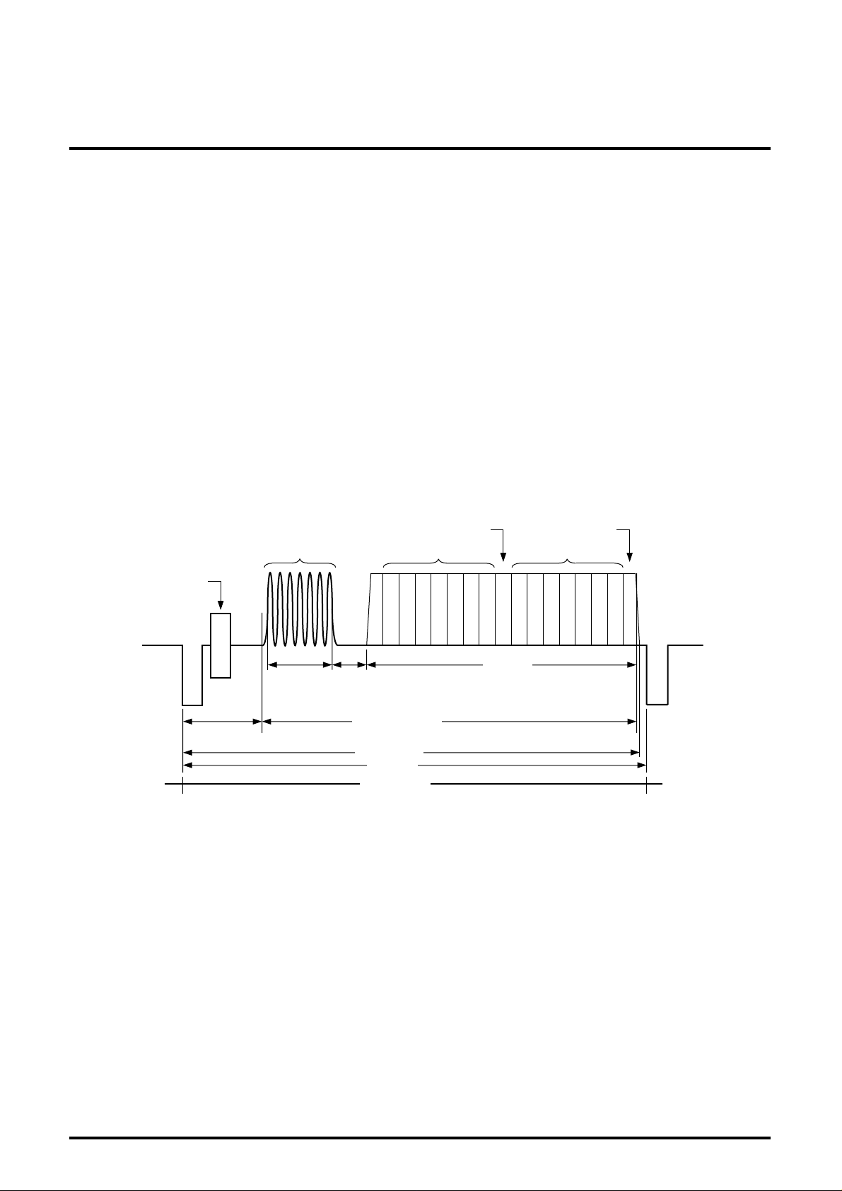
Closed Caption Encoding
In the NTSC (525/60) mode, 8-bit¥2byte data, including parity bit,
set in the register are converted into the format shown in fig. 1 and
then will be inserted in the video signal according to the register
data of the closed captions control specification (closed caption on/
off and caption data insertion mode). After the completion of
transmission, the new data are loaded in the register by setting the
close caption flag to "1", then the transferred data are loaded in the
register on the trailing edge of V-sync pulse by setting that flag to
"0". (In case the closed caption flag is "1", the new data loading is
halted and the caption data are not inserted in the video signals).
20(283) line
Color
Burst
10.500±0.5µs
7 cycles of 503kHz
(Clock Run-in ) 1st. byte 2nd. byte
CCD00
START BIT
12.910µs
3.972+0.2/-0.0µs
51.268+0.2/-0.0µs
61.331±0.5µs
63.556µs
21(284) line
Parity Bit Parity Bit
CCD03
CCD04
CCD05
CCD06
CCD07
CCD01
CCD02
CCD10
33.764µs
CCD11
CCD12
Fig. 1 CLOSED CAPTION WAVEFORM
CCD13
CCD14
CCD15
CCD16
CCD17
22(285) line
6
Page 7

MITSUBISHI ICs (TV)
PRELIMINARY
Notice:This is not a final specification.
Some parametric limits are subject to change.
CGMS (IEC 1880) Encoding
In the NTSC (525/60) mode, the 20-bit data, consisting of 14-bit
data including CRCC code and 6-bit error correction code
generated by the input data, are converted into the video format
Color
Burst
Ref Bit
bit 1
bit 2
2.232±50µs
bit 3
bit 4
Input Data
bit 5
M65675FP/M65676FP
DIGITAL NTSC/PAL ENCODER
shown in fig. 2 and then inserted in TV line 20/283, according to the
register data of CGMS control mode (CGMS on/off).
The transferred data are loaded to the register on the trailing edge
of V-sync, after a write-enable (WE) was set to "1".
CRCC
bit 6
bit 8
bit 9
bit 10
bit 11
bit 7
bit 12
bit 13
bit 14
bit 15
bit 16
bit 17
bit 18
bit 19
bit 20
70±10 IRE
11.2±0.3µs
63.556µs
20(283) line19(282) line
Fig. 2 CGMS WAVEFORM
WSS (ETS 300 294) Encoding
In the PAL (625/50) mode, 14-bit data, set in the register, is
modulated to the signal format shown in fig. 3 and then will be
inserted into TV line 23, according to the register data of WSS
Run in Start code
Color
Burst
1E3C1F1F1C71C7 group1
Aspect
Ratio
(4bit)
49.1±0.3µs
21(284) line
control mode (WSS on/off).
The new register data are loaded on the trailing edge of V-sync,
after a write-enable (WE) was set to "1".
Input Data
group2
Enhanced
Services
(4bit)
group3
Subtitles
(3bit)
group4
Others
(3bit)
"0"
200±10ns
500mV±5%
"1"
200±10ns
11.0±0.25µs
22 line
27.4±1.4µs
64.0µs
23 line
24line
Fig. 3 WSS WAVEFORM
7
Page 8

MITSUBISHI ICs (TV)
PRELIMINARY
Notice:This is not a final specification.
Some parametric limits are subject to change.
Color Subcarrier Generation
32-bit accuracy color subcarrier is generated from 27-MHz clock
signal according to the register data.
The subcarrier frequencies are as follows;
M-fsc mode=455fH/2
=3.579545MHz±10Hz
B-fsc_1 mode=1135fH/4
=4.43359375±5Hz
B-fsc_2 mode=1135f
Note:The above carrier frequencies are based on the input clock frequency of
27.0MHz. So, the generated subcarrier is also fluctuated according to a drift
of the external clock frequency.
Interpolation
The 13.5MHz data of Y, U and V are processed by an a v arage-v alue
interpolation and then each data rate are increased up to two times
that of 27.0MHz.
Chroma modulation
The selected subcarrier frequency, which generated 27.0MHz rate
U and V signals, is modulated.
Video Anticopy Signal Addition [2]
(Pseudo Sync/AGC/Back Porch Pulses)
This applies to M65675FP only.
The several anticopy signals (Pseudo Sync/AGC/Back Porch
Pulses), in accordance with Macrovision Video anticopy processes
Rev.7.01 dated Sep. 6, 1996, are inserted into the appropriate
video signals according to the register data. (This applies to
M65675FP only)
Video Anticopy Signal Generation
This applies to M65675FP only.
Several anticopy signals in accordance with Macrovision anticopy
processes Rev. 7.01 dated Sep. 6, 1996 are added to Y/C output
signals according to the I
For more information about Macrovision video anticopy processes,
please contact nearest MITSUBISHI Electric sales office.
The video anticopy specification is provided to only those
customers of MITSUBISHI Electric Corp. who have executed a
license or a non-disclosure agreement with Macrovision Corp.
Sample request and sales orders require the following procedure.
In the case of the customers who have no license.
◊Contact VP sales & marketing,ACP-PPV, Macrovision
Corporation.
Phone : USA (408) 743-8600
Fax : USA (408) 743-8610
◊Complete the appropriate agreement with Macrovision.
◊Then, inform to MITSUBISHI in writing that the agreement has
completed.
H/4+25Hz
=4.43361875±5Hz
2
C register data.
M65675FP/M65676FP
DIGITAL NTSC/PAL ENCODER
◊Samples will then be sent to customer after MITSUBISHI's
confirmation of it.
Sales Orders
◊ In case the customer has a Macrovision license:
The customer provides MITSUBISHI Electric Corp. with a written
confirmation of the license.
Customer can then purchases M65675FP.
◊ In case the customer does not have a Macrovision license:
The customer must obtain a license or waiver from Macrovision.
The customer must provide MITSUBISHI Electric Corp. with a
written confirmation of the license or waiver from Macrovision.
Customer can then purchases M65675FP.
Synchronization Control
Sync Signal Processing
The H/V sync signals are available in following 3 conditions; (1) in
synchronization with external sync signal, (2) in a slave mode which
refers to a digital blanking code and (3) in a master mode which
refers to a internally generated sync signal, according to the
register data. The timing specifications in each modes are as
follows;
◊ The slave mode
H-sync input condition: 1H =63.555 - 1.5/+10ms (525/60)
=64.0 - 1.5/+10ms (625/50)
V-sync input condition: 1V =262.5H±10H (525/60)
=312.5H±10H (625/50)
Field condition : Even-1/4H<Vsync<1/4H (Typical Vsync=
0H)
Odd 1/4H£Vsync£3/4H (Typical Vsync=
1/2H)
◊ The master mode
H-sync generation condition: 1H =63.555±0.035ms (525/60)
=64.0±0.035ms (625/50)
V-sync generation condition: 1V =262.5H±1/4H (525/60)
= 312.5H±1/4H (625/50)
Field condition : Even-1/4H<Vsync<1/4H (Typical
Vsync=0H)
Odd 1/4H£Vsync£3/4H (Typical
Vsync=1/2H)
Timing Signal Generation
A number of internal timing signals are generated with the trailing
edge of sync signals (shown in 4.2.1) as reference. All signals can
be adjusted in 13.5MHz-step up to ±1.2ms with respect to the
reference sync signal.
8
Page 9

MITSUBISHI ICs (TV)
PRELIMINARY
Notice:This is not a final specification.
Some parametric limits are subject to change.
Composite-sync Generation
The timing-corrected c-sync signal, for an addition to the Y signal, is
generated in accordance with RS170A (NTSC) and CCIR (PAL)
standards, as shown in fig. 4.
IRE
133
100
90
0.714V
0.286V
-40
cycle counts (13.5MHz)
peak level including chroma signal
20
4
0
white peak level
0H(reference point)
1.5±0.1µs
0.14±0.1µs
0 63 106127837 72
858
10.9±0.2µs
9.4±0.1µs
4.7±0.1µs
19 cycles
40
±2
9 cycles
set-up
7.5±2
0.14±0.2µs
2.3±0.1µs
0 31 3660
429 460 795429
cycle counts (13.5MHz)
M65675FP/M65676FP
DIGITAL NTSC/PAL ENCODER
Equalizing pulse Serrated pulse
0.14±0.2µs 0.14±0.2µs
4.7±0.1µs27.1µs
31.7775µs
31.7775µs
0.14±0.2µs
Fig. 4-1 NTSC HORIZONTAL SYNC SIGNAL (referred to EIARS170A)
IRE
133
100
90
0.7V
10
0.3V
-43
0.3±0.1µs
cycle counts (13.5MHz)
peak level including chroma signal
white peak level
0H(reference point)
50
0
1.5±0.3µs
0 63 107142844 76
864
12±0.3µs
5.6±0.1µs
4.7±0.2µs
0.2±0.1µs
43
±10%
10±1cycles
set-up
0-2
Fig. 4-2 PAL HORIZONTAL SYNC SIGNAL (referred to CCIR)
Serial Interface
The M65675FP/M65676FP has a serial data receiver, in
compliance with both typical and high speed modes, based on I
serial bus specification. The slave-address of it also responds to
two addresses of 40h and 42h. The address setting is done by
following procedure;
address setting pin DVASEL (pin 3) is "L" and "H" for the address of
40h and 42h, respectively.
The serial data are stored in the data register in the serial interface
block according to the appointed address after the receipt of the
2
Equalizing pulse Serrated pulse
0.2±0.1µs
2.35±0.1µs
0 32 3680
432 464 800432
cycle counts (13.5MHz)
0.2±0.1µs 0.2±0.1µs
62.0µs
4.7±0.2µs27.3µs
62.0µs
data. The stored data will be loaded to the registers in each internal
blocks at the timing of the first trailing edge of V-sync after the
transmission flag (WE) have been set up.
C
Analog Blocks
D-A Converter
The M65675FP/M65676FP has two 10-bit D-A converters. A
reference current of the D-A converters is supplied directly through
the Yref and Cref pins. The power save mode cuts the circuit
current. The maximum output amplitude is 1.2VP-P.
0.2±0.1µs
9
Page 10

MITSUBISHI ICs (TV)
PRELIMINARY
Notice:This is not a final specification.
Some parametric limits are subject to change.
Y and C Mixing Circuit
The analog outputs of D-A converters are filtered and then input to
the M65675FP again. The Y and C signals, whose maximum
amplitude is 0.6VP-P, are combined and the resulting composite
signal (CVBS) is output. The maximum amplitude of CVBS output is
1.2VP-P.
6-dB Amplifier
The M65675FP has three 6-dB amplifiers. The maximum input is
0.6VP-P and the resulting maximum output will be 1.24VP-P. The
maximum drivability and band width are 1mA and 6MHz,
respectively.
M65675FP/M65676FP
DIGITAL NTSC/PAL ENCODER
Operating Description
Initialize
After power-on, the M65675FP/M65676FP has two different
initialize sequences in the master and slave modes, respectively.
In the master mode, the internal registers are initialized responding
to the reset signal. After reset, the serial registers are set to the
default data and an internal control clock (13.5MHz) is generated
from the system clock.
In the slave mode, the internal registers are initialized the same as
in the master mode. The ser ial registers are set up to the default
data and the system clock generates the internal control clock (13.5
MHz) in the synchronization with the trailing edge of the horizontal
sync signal (H-sync), after reset. (Referring to Fig. 5)
In case the serial registers are set up to data other than the default
ones, the data should be renewed according to the I
in both the master and slave modes, after reset.
2
C bus format
·In the master modeÒ
System clock
(27.0MHz)
Reset
H-sync
·In the slave modeÒ
System clock
(27.0MHz)
Reset
H-sync
Generation starting timing
of reference clock
Generation starting timing
of reference clock
Fig. 5 GENERATION STARTING TIMING OF INTERNAL REFERENCE CLOCK
10
Page 11

MITSUBISHI ICs (TV)
PRELIMINARY
Notice:This is not a final specification.
Some parametric limits are subject to change.
M65675FP/M65676FP
DIGITAL NTSC/PAL ENCODER
Serial Register
The serial address register can be addressed by I2C bus.
The M65675FP/M65676FP has two slave addresses, 40 and 42h.
In the actual use, one of two is selected and then Pin 3 (DVASEL)
is set according to the selected address data
Slave address=40h
bit7 bit6 bit5 bit4 bit3 bit2 bit1 bit0
0100000R/W
42h
0100001R/W
Register Mapping and Description
sub
address
00 Write control WE P-save UVin YC
01
02 CC1F CC2F CCI/F CCD1 CCD0 CCIR1 CCIR0
03 Sync level sync7 sync6 sync5 sync4 sync3 sync2 sync1 sync0
04 Burst level burst6 burst5 burst4 burst3 burst2 burst1 burst0
05 Sync delay SD4 SD3 SD2 SD1 SD0
06 Y delay YD4 YD3 YD2 YD1 YD0
07 TINT TINT7 TINT6 TINT5 TINT4 TINT3 TINT2 TINT1 TINT0
08
09 CC116 CC115 CC114 CC113 CC112 CC111 CC110
0A
0B CC216 CC215 CC214 CC213 CC212 CC211 CC210
0C
0D
0E OSD control CLTEN
0F
10 CTB13 CTB12 CTB11 CTB10 CTB03 CTB02 CTB01 CTB00
11 CTR13 CTR12 CTR11 CTR10 CTR03 CTR02 CTR01 CTR00
12 CTY33 CTY32 CTY31 CTY30 CTY23 CTY22 CTY21 CTY20
13 CTB33 CTB32 CTB31 CTB30 CTB23 CTB22 CTB21 CTB20
14 CTR33 CTR32 CTR31 CTR30 CTR23 CTR22 CTR21 CTR20
15 CTY53 CTY52 CTY51 CTY50 CTY43 CTY42 CTY41 CTY40
16 CTB53 CTB52 CTB51 CTB50 CTB43 CTB42 CTB41 CTB40
17 CTR53 CTR52 CTR51 CTR50 CTR43 CTR42 CTR41 CTR40
18 CTY63 CTY62 CTY61 CTY60
19 CTB63 CTB62 CTB61 CTB60
1A CTR63 CTR62 CTR61 CTR60
1B
1C
1D
1E
1F
20
Interface
Closed Caption (1st field)
Closed Caption (2nd field)
CGMS/WSS
Color Lookup Table
∗1
Macrovision
Function
76543210
525/
NTSC/
625
CC106 CC105 CC104 CC103 CC102 CC101 CC100
CC206 CC205 CC204 CC203 CC202 CC201 CC200
CG08/
WS07
CTY13 CTY12 CTY11 CTY10 CTY03 CTY02 CTY01 CTY00
Mode selection N16 [0] N0 [6] N0 [5] N0 [4] N0 [3] N0 [2] N0 [1] N0 [0]
Color Stripe
Definition #1
Color Stripe
Definition #2
Color Stripe
Definition #3
Color Stripe
Definition #4
Color Stripe
Definition #5/6/7
N21 [1] N21 [0] N1 [5] N1 [4] N1 [3] N1 [2] N1 [1] N1 [0]
N7 [1] N7 [0] N6 [2] N6 [1] N6 [0] N5 [2] N5 [1] N5 [0]
CG07/
WS06
YC/UV SCH offset Setup1 Setup0
PAL
CG06/
WS05
CG14/
WS13
N2 [5] N2 [4] N2 [3] N2 [2] N2 [1] N2 [0]
N3 [5] N3 [4] N3 [3] N3 [2] N3 [1] N3 [0]
N4 [6] N4 [5] N4 [4] N4 [3] N4 [2] N4 [1] N4 [0]
data
INV CbCrINV
CG05/
WS04
CG13/
WS12
CG04/
WS03
CG12/
WS11
OSD
CLK
Color
Bar
CG03/
WS02
CG11/
WS10
BLD
mode
CG02/
WS01
CG10/
WS09
BLD1 BLD0
CGMS
/WSS
CG01/
WS00
CG09/
WS08
11
Page 12

MITSUBISHI ICs (TV)
PRELIMINARY
Notice:This is not a final specification.
Some parametric limits are subject to change.
Register Mapping and Description
sub
address
21
22
23
24
25
26
27
28
29
2A
2B
2C
2D
*1 : These registrs are M65675FP only
∗1
Macrovision
Function
(cont.)
Pseudo-sync
parameter #1
Pseudo-sync
parameter #2
Pseudo-sync
parameter #3
Pseudo-sync/AGC
pulse line select
Pseudo-sync/AGC
pulse A/B select
Pseudo-sync/AGC
on/off FormatA
Pseudo-sync/AGC
on/off FormatB
Back Porch pulse
configuration
Start to 1st/1st to 2nd
Phase Switch Point
2nd to End Phase
Switch Point/
Subcarrier Phase
Colorstripe line
phase
M65675FP/M65676FP
DIGITAL NTSC/PAL ENCODER
data
76543210
N8 [5] N8 [4] N8 [3] N8 [2] N8 [1] N8 [0]
N9 [5] N9 [4] N9 [3] N9 [2] N9 [1] N9 [0]
N10 [5] N10 [4] N10 [3] N10 [2] N10 [1] N10 [0]
N11 [7] N11 [6] N11 [5] N11 [4] N11 [3] N11 [2] N11 [1] N11 [0]
N11 [14] N11 [13] N11 [12] N11 [11] N11 [10]
N12 [7] N12 [6] N12 [5] N12 [4] N12 [3] N12 [2] N11 [1] N12 [0]
N12 [14] N12 [13] N12 [12] N12 [11] N12 [10]
N13 [7] N13 [6] N13 [5] N13 [4] N13 [3] N13 [2] N13 [1] N13 [0]
N14 [7] N14 [6] N14 [5] N14 [4] N14 [3] N14 [2] N14 [1] N14 [0]
N15 [7] N15 [6] N15 [5] N15 [4] N15 [3] N15 [2] N15 [1] N15 [0]
N18 [3] N18 [2] N18 [1] N18 [0] N17 [3] N17 [2] N17 [1] N17 [0]
N20 [2] N20 [1] N20 [0] N19 [3] N19 [2] N19 [1] N19 [0]
N21 [9] N21 [8] N21 [7] N21 [6] N21 [5] N21 [4] N21 [3] N21 [2]
N11 [9] N11 [8]
N12 [9] N12 [8]
Register Functional Description
Sub
address
00
01
Name Function Remark
WE
P-save
UVin
INV
Y/C
INV
Cb/Cr
Color Bar
525/625
NTSC/PAL
YC/UV
SCH
Register Write Enable
"0" write disable
"1" write enable
Power Down Control
"0" power down "off"
"1" power down "on"
Input Video Data Format Selection
"0" Y/U/V input
"1" Y/Cb/Cr input
Pixel Data Sep. Timing Control (Y/C)
"0" Y/C separation in inverted timing
"1" Y/C separation in non-inverted timing
Pixel Data Sep. Timing Control (Cb/Cr)
"0" Y/C separation in inverted timing
"1" Y/C separation in non-inverted timing
Color Bar Generation Control
"0" color bar generation "off"
"1" color bar generation "on"
Input Pixel Data Field Frequency Setting
"0" 525/60 field
"1" 625/50 field
Line Phase Inversion Control in V-axis
"0" Phase Inversion "off" (NTSC)
"1" Phase Inversion "on" (PAL)
Selection of DAC Output
"0" Y/C output
"1" U/V output
SCH Phase Control
"0" SCH Phase Control "on"
"1" SCH Phase Control "off"
Default
Data
20h
Color look-up table
should be initialized.
03h
12
Page 13

MITSUBISHI ICs (TV)
PRELIMINARY
Notice:This is not a final specification.
Some parametric limits are subject to change.
M65675FP/M65676FP
DIGITAL NTSC/PAL ENCODER
Register Functional Description (cont.)
Sub
address
01
02
02
03 sync (7:0) Sync Signal Output Level Setting DBh
04 burst (6:0) Burst Level Setting 54h
05 SD (4:0) Composite Sync Multiplexing Timing Setting 19h
06 YD (4:0) Luma Signal Delay Setting 04h
07 TINT (7:0) Chroma Output TINT Control 00h
08 CC10 (6:0) 1st Byte Data Setting for Field 1 00h
09 CC11 (6:0) 2nd Byte Data Setting for Field 1 00h
0A CC20 (6:0) 1st Byte Data Setting for Field 2 00h
0B CC21 (6:0) 2nd Byte Data Setting for Field 2 00h
0C
:
0D
0E
0E BLD (1:0)
0F
:
1A
1B
:
2D
Name Function Remark
offset
CGMS/WSS
CC1F Closed Caption Data Transmission Flag in Field 1.
CC2F Closed Caption Data Transmission Flag in Field 2.
CCI/F
CCD (1:0)
CCIR (1:0)
CG (14:1)
[WS (13:0)]
CLTEN
OSDCLK
BLD mode
CTY (00:63)
CTB (00:63)
CTR (00:63)
N0
:
N21
fsc Offset Frequency (25Hz) Control
"0" offset no-addition
"1" offset addition
7.5IRE Setup Control
"00" setup "off"
"01" +7.5IRE setup
"1X" -7.5IRE setup
CGMS/WSS Generation Control
"0" CGMS/WSS generation "off"
"1" CGMS/WSS generation "on"
Closed Caption Interface Setting
"0" internal generation mode
"1" external input mode
Closed Caption Generation Setting
"00" generation "off"
"01" generation for only field 1
"10" generation for only field 2
"11" reserved
Input Pixel Data Format Setting
"00" CCIR656
"01" 8bit CCIR601
"10" 16bit CCIR601
"11" reserved
CGMS or WSS Data Setting 00h
CLT Data Renewing Enable
"0" disable
"1" enable
OSDCLK Frequency Setting
"0" 6.75MHz
"1" 13.5MHz
Blending Mode Setting
"0" Y and C are mixing
"1" Only Y is mixing
Blending Color Address Setting
"00" blending "off"
"01" CLT0 is set for a blending color
"10" CLT(1:0) is set for a blending Color
"11" CLT(2:0) is set for a blending color
Color Look-up table RAM Setting 00h
Macrovision Setting 00h
It have to set "1"
in the setting of
525/625=0
It is active in the
setting of 525/625=0.
CGMS/WSS
selection is depend
on 525/62 setting.
In the case of "1",
C is equal to the
OSD setting color.
Default
Data
03hsetup (1:0)
00h
00h
00h
00h
00h
13
Page 14

MITSUBISHI ICs (TV)
PRELIMINARY
Notice:This is not a final specification.
Some parametric limits are subject to change.
DESCRIPTION OF PIN
Pin No. Pin name Type Function
1DVSS2 Supply Digital ground for I/O.
2 PXCLK O
3 DVASEL I
4 HD I/O
5 VD I/O
6 VD9
7 VD8
8 VD7
9 VD6
10 VD5
11 VD4
12 VD3
13 VD2
14 VD1
15 VD0
16 DV
17 DVDD2 Supply Digital positive supply for I/O.
18 DVDD1 Supply Digital positive supply for internal logic.
19 DVSS1 Supply Digital Ground for internal logic.
20 OSDCK O
21 OSD0
22 OSD1
23 OSD2
24 Master/Slave I
25 RESET I Asynchronous reset, active "LOW".
26 ACK O Acknowledge line (Open drain output).
27 SDA I/O Serial data line/Acknowledge line (Open drain output).
28 SCL I Serial clock line.
29 TEST I
30 DV
31 N.C. No connection.
32 N.C. No connection.
33 C O
34 N.C. No connection.
35 CVBS O
36 AVSS2 Supply Analog ground for 6-dB amplifiers.
37 Y O
38 AVDD2 Supply Analog positive supply for 6-dB amplifiers.
39 Yin I
40 N.C. No connection
41 Cin I
SS2 Supply Digital ground for I/O.
DD1 Supply Digital positive supply for internal logic.
Reference clock for pixel data input.
The clock frequency is 27.0MHz or 13.5MHz in CCIR656/8-bit CCIR601 or 16-bit CCIR601 input
mode, respectively.
2
C slave address setting.
I
"Low" is for the slave address of 40h.
"High" is for the slave address of 42h.
Horizontal sync signal.
It is an input or output in the slave or master mode, respectively.
Vertical sync signal.
It is an input or output in the slave or master mode, respectively.
Video data inputs.
The input video data are the luma (Y) data as defined in CCIR Rec 601 in 16-bit CCIR601 mode.
I/O
In the Y/U/V output mode, the output is 10-bit luma signal with a composite sync.
In 16-bit CCIR601 mode, an MSB and LSB is VD7 and VD0, and in the Y/U/V output mode, VD9 and
VD0, respectively.
Reference clock for the external OSD microprocessor.
The frequency is 13.5MHz or 6.25MHz, alternated by I
Color Look-up table address input.
I
MSB and LSB is OSD2 and OSD0, respectively.
Synchronizing mode selection.
"Low" is for the slave mode.
"High" is for the master mode.
Test mode control.
It should be grounded during actual use.
The analog chroma output signal from 6-dB amplifier.
The output amplitude is 1.0V
The analog composite video output signal from 6-dB amplifier.
The output amplitude is 1.24V
The analog luma output signal from 6-dB amplifier.
The output amplitude is 1.2V
The analog luma input from an external LPF.
This input has clamp circuit. The signal must input via capacitor.
The analog chroma input from an external LPF.
This input has bias circuit. The signal must input via capacitor.
P-P (typ.), while the input one is 0.5VP-P.
P-P (typ.).
P-P (typ.), while the input one is 0.6VP-P.
M65675FP/M65676FP
DIGITAL NTSC/PAL ENCODER
2
C bus control.
14
Page 15

MITSUBISHI ICs (TV)
PRELIMINARY
Notice:This is not a final specification.
Some parametric limits are subject to change.
DESCRIPTION OF PIN (cont.)
Pin No. Pin name Type Function
42 Ccomp I
43 DAC O
44 AV
45 AV
46 DAY O
47 Cref I
48 Yref I
49 Ycomp I
50 N.C. No connection.
51 DV
52 DVSS1 Supply Digital ground for internal logic.
53 Xout O
54 Xin I
55 DV
56 PXD7
57 PXD6
58 PXD5
59 PXD4
60 PXD3
61 PXD2
62 PXD1
63 PXD0
64 DVDD2 Supply Digital positive power supply for I/O
DD1 Supply Analog positive supply for D/A converters.
SS1 Supply Analog ground for D/A converters.
DD1 Supply Digital positive power supply for internal logic.
SS2 Supply Digital ground for I/O.
Phase compensation for chroma or V D/A converters.
It should be connected to the analog ground via a capacitor.
Chroma or V signal output.
It should be connected to the analog supply via a resistor (RL).
The output amplitude is set up by reference resistor (Rref) and RL.
Luma or V signal output.
It should be connected to the analog supply via a resistor (RL).
The output amplitude is set up by reference resistor (Rref) and RL.
Reference current control for chroma or V D/A converter.
It should be connected to the analog supply via a reference resistor (Rref).
Reference current control for luma or U D/A converter.
It should be connected to the analog supply via a reference resistor (Rref).
Phase compensation for luma or U D/A converters.
It should be connected to the analog ground via a capacitor.
System clock output.
It should be in no connection except that it is connected to a X'tal oscillator.
System clock input.
The clock frequency is 27.0MHz only.
Pixel data inputs.
The acceptable video data are;
multiplexed video data (Y/Cb/Cr) including timing reference code of SAV and EAV as defined in
I
CCIR Rec656, and multiplexed video data (Y/Cb/Cr) as defined in CCIR Rec601, and multiplexed
Color difference signals (Cb/Cr).
An MSB and LSB is PXD7 and PXD0, respectively.
M65675FP/M65676FP
DIGITAL NTSC/PAL ENCODER
Interface
The M65675FP/M65676FP has two interfaces as follows;
Pixel data interface
OSD interface
Pixel Data Interface
The M65675FP/M65676FP accepts these 6 digital pixel data
formats as shown below;
In CCIR656
Y and Cb/Cr, in a digital video transmission format
Y and U/V, in a time multiplexed 8-bit serial data format
In CCIR601
Y and Cb/Cr, in a digital video transmission format
Y and U/V, in a time multiplexed 8-bit serial data format
Y, in a digital video transmission format and time multiplexed
Cb/Cr
Y and U/V, in a time multiplexed 16-bit serial data format
The 8-bit serial data in CCIR656 and CCIR601 are taken into the
15
M65675FP/M65676FP through PXDATA [7:0] ports synchronizing
with a pixel clock (PXCLK) generated by the LSI. In the case of
CCIR601 16-bit serial data, 8-bit color difference signals (Cb/Cr or
U/V) and luma signal (Y) are taken into the LSI synchronizing with
pixel clock (PXCLK) through PXD [7:0] and VD [7:0] port,
respectively.
CCIR656 pixel data are accepted in only the slave mode, while
CCIR601 ones are accepted in both the master and slave modes.
In the case of CCIR656 pixel data, H/V sync and a field
identification signals are regenerated internally referring to SAV and
EAV code multiplexed in the pixel data. In the case of CCIR601
pixel data, H/V sync and the field identification signals are
regenerated internally, then the H and V sync signals are available
via HD and VD ports in the master mode operation, respectively.
Moreover, in the slave mode, the M65675FP/M65676FP is in the
slave operation synchronized with H/V sync signals via HD/VD
ports and a field identification is done using the H/V sync input
signals.
Page 16

MITSUBISHI ICs (TV)
PRELIMINARY
Notice:This is not a final specification.
Some parametric limits are subject to change.
The pixel data interface pin assignment is shown in Table 1.
M65675FP/M65676FP
DIGITAL NTSC/PAL ENCODER
Table 1 Pixel Data Interface Pin Assignment
Pin name I/O Function
PXCLK O
(Note1) I/O Horizontal sync signal. Input in the slave or output in the master mode.
HD
VD (Note1) I/O Vertical sync signal. Input in the slave or output in the master mode.
PXD [7:0] I
PD [7:0] I
Note1 : In CCIR656 mode, H sync and V sync generated by EAV will be output via terminals HD and VD, respectively.
Pixel clock output.
In the case of CCIR656 / CCIR601 8-bit data and CCIR601 16-bit inputs, this will be a free-run clock of 27MHz and
13.5MHz, respectively.
Pixel data input.
8-bit data input in CCIR656 / CCIR601 or the color differential signals (Cb/Cr) input in CCIR601 16-bit data format.
Pixel data input.
Luma (Y) data input in CCIR601 16-bit data format.
OSD Interface
The OSD data, which are storaged in the address assigned by the
color look-up table RAM (CLT-RAM) address data input via OSD
[2:0] ports, are multiplexed into the Y signal synchronizing with OSD
clock (OSDCK) delivered from the M65675FP/M65676FP.
The OSD interface pin assignment is shown in Table 2.
Table 2 The OSD interface Pin assignment
Pin name I/O Function
OSDCK O
OSD [2:0] I Color look-up table RAM address input.
OSD clock output.
13.5MHz free-run clock or 6.25MHz H-start-and-stop clock.
16
Page 17

MITSUBISHI ICs (TV)
PRELIMINARY
Notice:This is not a final specification.
Some parametric limits are subject to change.
M65675FP/M65676FP
DIGITAL NTSC/PAL ENCODER
APPLICATION EXAMPLE
A typical application diagram of the M65675FP/M65676FP together with the M65773FP 1-chip MPEG2 decoder is shown in Figure 6.
Y
C
CVBS
75Ω
75Ω
75Ω
0.1µF
220µF
Stage
300Ω
DAY
220µF
75Ω
Driver
2.2µF
2.2µF
Y
Y in
RESET
OSD(2:0)
OSDCK
ACK
SDA
SCL
SCL
SDA/ACK
RESET
AO0
AO1
AO2
AO3
LRCLK
DOCLK
DACCLK
ACLKO
ACLKI
BDER
0.1µF
C
2.2µF
CVBS
3
47µF
0.01µF
R/G/B
OSC1
OSD micro
computer
M35041
HDVDCS
VDD
RESET
VSS
SCK
SIN
Audio out (L)
Audio out (R)
Lch
Rch
Audio
DAC
LRCIN
DIN
XTI
BCKIN
47µF
0.01µF
47µF
0.01µF
27MHz
16M
SDRAM
2.2µF
DD
AVss
AV
Ccomp
TEST
Master/Slave
DVASEL
DVSS
DV
DD
X out
X in
47µF
0.01µF
27MHz
XO
2.2µF
0.1µF
Ycomp
VD(9:0)
VSS
VDD
CLK in
10kΩ
0.1µF
10kΩ
Yref
Cref
Digital
NTSC/PAL
Encoder
M65675FP
M65676FP
PXD(7:0)
8
PXD
PXCLK
MPEG2
System/
Video/Audio
Decoder
M65773FP
BD
1kΩ
Stage
Filter
Filter
300Ω
0.1µF
C in
DAC
PXCLKHDVD
VSYNC
HSYNC
BCLK
BDEN
BDREQ
17
8
BD
RCLK
BDEN
BDER
BDREQ
Chanel
Decoder
: 3.3V Supply for Analog/Digital
(Note 1) Connect a tantalum or electrolytic capacitor of 10µF or more and a ceramic
capacitor of 0.01µF each in parallel between DV
These capacitors should be placed as possible to the device.
(Note 2) In case several LSIs are connected to an I2C bus, SDA and ACK at power-down
should be tied externally in a situation when only M65675FP/M65676FP is power-off.
DD/AVDD and DVss/AVss pins.
3.3kΩ
CS
SCK
RESET
Host
CPU
Fig. 6 TYPICAL APPLICATION DIAGRAM
SIN
Units Resistance : Ω
Capacitance : F
 Loading...