

Page 1
×
×
∗
∗
MITSUBISHI ICs (TV)
PRELIMINARY
Notice:This is not a final specification.
Some parametric limits are subject to change.
DESCRIPTION
The M65667SP is a NTSC PIP (Picture in Picture) signal
processing LSI, whose sub and main-picture inputs are composite
and Y/C separated signals, respectively. The built-in field memory
(96k-bit RAM) ,V-chip data slicer and analog circuitries lead the PIP
system low cost and small size.
FEATURES
•
Built-in 96k-bit field memory (sub-picture data storage)
•
Internal V-chip data slicer (for sub-picture)
•
Pin compatible with M65617SP
•
Vertical filter for sub-picture (Y signal )
•
Single sub-picture (selectable picture size : 1/9 , 1/16)
•
Sub-picture processing sepecification (1/9 size / 1/16 size) :
Quantization bits Y, B-Y, R-Y : 6bits
Horizontal sampling 171 pixels (Y) , 28.5 pixels (B-Y, R-Y)
Vertical lines 69/ 52 lines
•
Frame (sub-picture) on/off
•
Built-in analog circuits :
Two 8-bit A/D converters (main and sub-picture signals)
Two 8-bit D/A converters (Y and C sub-picture signals)
Sync-tip-clump, VCXO, Analog switch ... etc.
2
I
C BUS control (parallel/serial control) :
•
PIP on/off , Sub-picture size(1/9 or 1/16), Frame on/off
(programmable luma level), PIP position (4 corners fixed
position), Picture freeze , Y delay adjustment, Chroma lev el, Tint,
Black level, Contrast ... etc.
APPLICATION
NTSC color TV
RECOMMENDED OPERATING CONDITION
Supply voltage range........................................................3.1 to 3.5V
Operating frequency.........................................................14.32 MHz
Operating temperature....................................................-20 to 75 ° C
Input voltage (CMOS interface)"H"........................V
"L".............................0 to V
Output current (output buffer)........................................ ± 4mA (MAX)
Output load capacitance............................................20pF (MAX)
Circuit current.........................................................................160mA
DD
0.7 to V
DD
DD
0.3V
PICTURE-IN-PICTURE SIGNAL PROCESSING
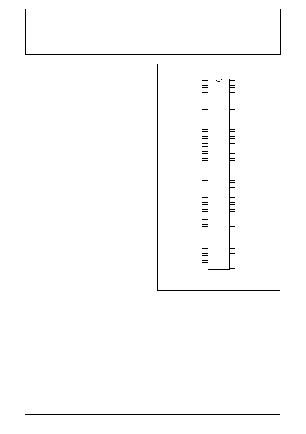
PIN CONFIGURATION (TOP VIEW)
AVss3 (vcxo)
VCXO out
VCXO in
FILTER
AVdd3 (vcxo)
AVdd2 (m)
Vin (m)
Vrt (m)
Vrb (m)
AVss2 (m)
AVdd1 (s)
Vrb (s)
AVss1 (s)
RESET
DVdd1
BGP(s)/TEST0
CSYNC(s)/TEST1
DVss2 (ram)
V
1
BIAS
Vin (s)
Vrt (s)
DVss1
SCK
ACK
DATA
CLK
1
2
3
4
5
6
7
8
9
10
11
12
13
14
15
16
17
18
19
20
21
22
23
24
25
26
Outline 52P4B
M65667SP
52
AVssf (ana)
51
Cin
50
TESTEN
49
Yin
TEST9
48
Y-PIP
47
TEST8
46
45
C-PIP
44
AVdd4 (da)
43
C-PIPin
AVss4 (da)
42
M65667SP
41
Y-PIPin
40
ADJ-Ysub
39
Yout-sub
38
ADJ-Csub
37
Cout-sub
36
DVss3
35
DVdd3
34
LOCK/TEST7
33
VD/CSYNC/TEST6
HD/TEST5
32
31
SWM/TEST4
30
MCK
29
fsc/TEST3
BGP(m)/TEST2
28
DVdd2 (ram)
27
NOTICE: Connect a 0.1 µ F or larger capacitor between V
pins.
1 : Include pin capacitance (7pF)
DD
and V
SS
1
Page 2
MITSUBISHI ICs (TV)
PRELIMINARY
Notice:This is not a final specification.
Some parametric limits are subject to change.
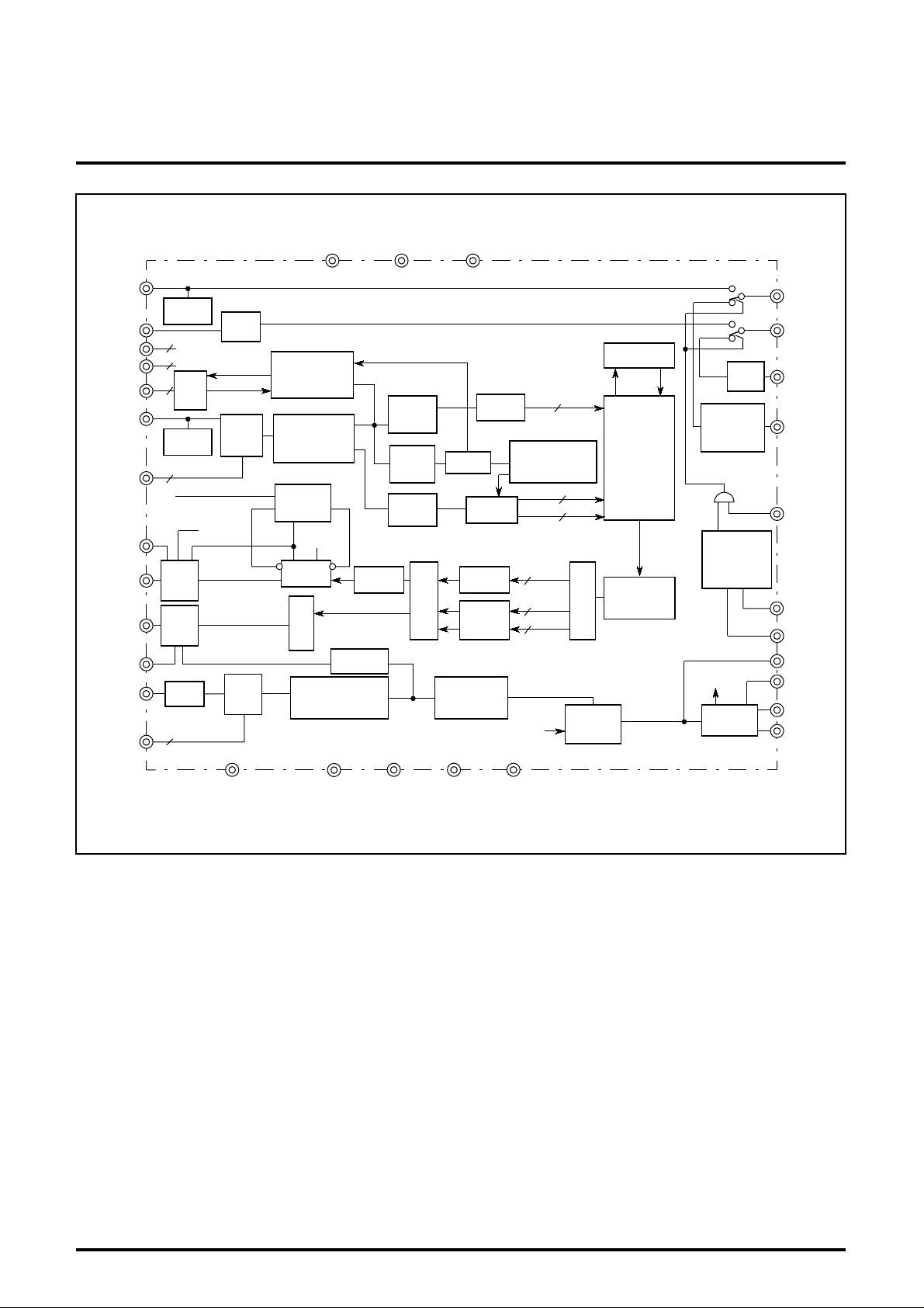
BLOCK DIAGRAM
Yin
Sync tip
Cin
Vdd / Vss
for test
DATA
CLK
ACK
Vin(s)
Vrt(m)
Vrb(m)
ADJ-Ysub
Yout-sub
Cout-sub
ADJ-Csub
Vin(m)
Vrt(m)
Vrb(m)
15
3
3
2
HD
2
Clamp
Sync tip
Clamp
D/A
8bit
D/A
8bit
Bias
I2C
I/F
Bias
A/D
8bit
2
C )
( I
A/D
8bit
HPLL
SCK
V-chip
data slicer
Y/C SEP
(LPF,BPF)
Phase
Select
4fsc
Delay
fsc
Encode
Burst Data
Sampling
Y
Level
Detect
CSYNC(s)
/TEST1
C
Delay
Luma
Clamp
Sync
Sep
Demod
MIX
M65667SP
PICTURE-IN-PICTURE SIGNAL PROCESSING
BGP(s)
/TEST0
RAM(1H)
Bias
C
Y6
Timing Gen
(Decode)
B-Y
R-Y
6Y
B-Y
6
R-Y
6
6
6
Demux
VCXO
Driver
Vert-filter
&
MUX
Y
B-Y
R-Y
RAM
96Kbits
Back Porch
Clamp
Timing Gen
(Memory
Cont)
4fsc
VCXO
Delay
AFC
Tint
Delay
LPF
&MPY
Phase
Detect
Lock/Free-run
via I
2
Y- PIP
C- PIP
C- PIPin
Y- PIPin
SWMG
/TEST7
VD
/CSYNC
/TEST6
HD
/TEST5
FILTER
BIAS
VCXO in
VCXO out
RESET
MCK
BGP(m)
/TEST2
fsc
/TEST3
SWM
/TEST4
2
Page 3

MITSUBISHI ICs (TV)
PRELIMINARY
Notice:This is not a final specification.
Some parametric limits are subject to change.
PICTURE-IN-PICTURE SIGNAL PROCESSING
M65667SP
DESCRIPTION OF PIN
Pin No. Name I/O Function Remarks
1 AVss3
(VCXO)
2 VCXO out O VCXO output signal
3 VCXO in I VCXO input signal
4 FILTER I Filter
5 BIAS O Bias
6 AVdd3
(VCXO)
7 AVdd2 (m) Vdd Connect to analog power supply
8 Vin (m) I Chroma signal input (main-picture)
9 Vrt (m) O A/D Vref+ (main-picture)
10 Vrb (m) O A/D Vref- (main-picture)
11 AVss2 (m) GND Connect to analog GND
12 AVdd1 (s) Vdd Connect to analog power supply
13 Vin (s) I Composite video signal input (sub-picture)
14 Vrt (s) O A/D Vref+ (sub-picture)
15 Vrb (s) O A/D Vref- (sub-picture)
16 AVss1 (s) GND Connect to analog GND
17 RESET I Power on reset input signal ("L" reset)
18 DVss1 GND Connect to digital GND
19 DVdd1 Vdd Connect to digital power supply
20
BGP(s)/TEST0
21 SCK I For test (connect to digital GND) connect to GND
CSYNC(s)/TEST1
22
23 ACK O
24 DATA I
25 CLK I
26 DVss2(ram) GND Connect to digital GND
27 DVdd2(ram) Vdd Connect to digital power supply
BGP(m)/TEST2
28
29 fsc/TEST3 I(/O) For test (pull down to digital GND by resistor 15k Ω ) pull down 15k Ω
30 MCK I For test (connect to digital GND) connect to GND
31 SWM/TEST4 (I/)O For test non connect
32 HD/TEST5 I(/O) Horizontal sync input signal (Positive going edge is used)
VD/CSYNC
33
/TEST6
SWMG/TEST7
34
35 DVdd3 Vdd Connect to digital power supply
36 DVss3 GND Connect to digital GND
37 Cout-sub O D/A output signal (Chroma signal of sub-picture)
38 ADJ-Csub I D/A adjust for chroma signal (sub-picture)
39 Yout-sub O D/A output signal (Luma signal of sub-picture)
40 ADJ-Ysub I D/A adjust for luma signal (sub-picture)
41 Y-PIPin I PIP luma signal re-input
42 AVss4 (da) GND Connects to analog GND
43 C-PIPin I PIP chroma signal re-input
44 AVdd4 (da) Vdd Connect to analog power supply
45 C-PIP O PIP chroma signal output
46 TEST8 I For test (connect to analog GND) pull up 15k Ω
47 Y-PIP O PIP luma signal output
48 TEST9 I For test (connect to analog GND) connect to GND
49 Yin I Luma input signal (main-picture)
50 TESTEN I For test (connect to analog GND) connect to GND
51 Cin I Chroma input signal (main-picture)
52 AVssf (ana) Vss Connect to analog GND
GND Connects to analog GND
Vdd Connect to analog power supply
100k Ω to V
(I/)O For test non connect
I(/O) For test (connect to digital GND) pull down 15k Ω
2
I
C bus-data/Acknowledge output signal
2
I
C bus-data input signal
2
I
C bus-clock input signal
(I/)O For test non connect
I(/O) Vertical sync input signal (active "H")
I(/O) Enable input signal to display sub picture ("H" enable) pull up 15k Ω
,10 µ F to GND
DD
3
Page 4

∗
( ∗
−
−
−
−
−
−
|
−
−
−
−
MITSUBISHI ICs (TV)
PRELIMINARY
Notice:This is not a final specification.
Some parametric limits are subject to change.
(V
SS
ABSOLUTE MAXIMUM RATINGS
Symbol Parameter
V
DD3
V
I
V
O
O
I
P
d
T
opr
T
stg
1: Output current per output terminal. But P
DC CHARACTERISTICS
Supply voltage (3.3V) -0.3 4.6 V
Input voltage -0.3
Output voltage -0.3
Output current
1)
Power dissipation
Operating temperature -20 75 ° C
Storage temperature -50 125 ° C
d
(Ta=25 ° C, unless otherwise noted, V
=0V)
limits all current.
Limits
Min. Max.
V
V
−
I
I
OH
−
Symbol Parameter Test conditions
V
IL
V
IH
V
T
-
V
T
+ + 1.4
V
H
V
OL
V
OH
I
OL
I
OH
I
IH
I
IL
I
OZL
I
OZH
Input voltage
(CMOS interface)
Input voltage schmitt trigger
(CMOS interface)
Output voltage
Output current
Input current
Output leakage current
LV
HV
DD
=2.7V 0
DD
=3.6V 2.52
–
DD
=3.3V
V
Hysteresis
L
V
DD
H 3.25
LV
HV
LV
HV
LV
HV
=3.3V, | I
DD
=3.0V , V
DD
=3.0V , V
DD
=3.6V , V
DD
=3.6V , V
DD
=3.6V , V
DD
=3.6V , V
CI Input pin capacitance
CO Output pin capacitance − 7 15 pF
f=1MHz, VDD=0V
PICTURE-IN-PICTURE SIGNAL PROCESSING
Unit
+0.3
DD3
DD3
OL
=20
=-26
1400 mW
V
+0.3
V
mA
SS
=0V)
O
<1 µ A
OL
=0.4V 4
OH
=2.6V
I
=0V -1
I
=3.6V -1
O
=0V -1
O
=3.6V -1
M65667SP
Limits
Min. Typ. Max.
0.81 V
3.6 V
0.5
0.3
−−
−−
− 7 15 pF
1.65 V
2.4 V
1.2 V
0.05 V
−−
−−
-4 mA
1 µ A
1 µ A
1 µ A
1 µA
CIO Bidirectional pin capacitance − 7 15 pF
IDD Operating current
3.3V supply
−− 140 mA
Unit
V
mA
TYPICAL CHARACTERISTICS
THERMAL DERATING (MAXIMUM RATING)
2000
1600
1490
1200
800
400
POWER DISSIPATION Pd (mW)
0
0 25 75 125
AMBIENT TEMPERATURE Ta (°C)
50
100
4
Page 5

MITSUBISHI ICs (TV)
PRELIMINARY
Notice:This is not a final specification.
Some parametric limits are subject to change.
APPLICATION EXAMPLE
68p
PIP Luma signal output
Luma signal input (main-picture)
Chroma input signal (main-picture)
104104
PIP Chroma signal output
Ana.
10µ
103
Ana.
15k
104
104
150p
103
M65667SP
PICTURE-IN-PICTURE SIGNAL PROCESSING
Ana.
470
Vertical sync input signal (main-picture)
Horizontal sync input signal (main-picture)
Ana.
360
103
Sub-picture displaying on/off
Dig
10µ
103
3035404550
15k
Dig
2752
103
10µ
Digital +3.3V
power supply
Digital GND
Ana.
Analog +3.3V
power supply
Analog GND
Composite video
input signal
(sub-picture)
M65667SP
1 26
14p
51
330
104
5101520
470k
10µ
103
103
100k
2k
3.3µ
Ana.
104
Ana.
SYNC SEP
CIRCUIT
(OPTIONAL)
103
10µ
103
103
Ana.
104
10µ
103
103103
100k
10µ
Dig
330
560
Dig5V
47k
100
12k
100
Dig5V
47k
10k
SDA
12k
100
SCL
10k
2
C BUS Clock
I
input signal
I2C BUS DATA
input /output
signal
Separate Y/C signals by using LC-tank circuit or LPF,BPF for Y/C signals level adjust.
And then mix both signals for sub-picture input video signal.
Units Resistance : Ω
Capacitance : F
5
Page 6

MITSUBISHI ICs (TV)
PRELIMINARY
Notice:This is not a final specification.
Some parametric limits are subject to change.
PIP TV SYSTEM BLOCK DIAGRAM
(BASIC)
Composite
Video Signal
Y/C Separated
Video Signal
Y/C
Separation
Y
C
Y
C
Y
C
CV
M65667SP
PICTURE-IN-PICTURE SIGNAL PROCESSING
M65667SP
BLPLL
B-LD
PIP Signal
Processing
Y
C
Y
C
Video
Signal
Processing
Deflection
Unit
HD VD
Yoke
(Driving Method and Operating Specification for
Serial Interface Data)
(1) Serial data transmission completion and start
A low-to-high transition of the DATA (ser ial data) line while the CLK
(serial clock) is high, that completes the serial transmission and
makes the bus free.
A high-to-low transition of the DATA line while the CLK is high, that
starts the serial transmission and waits for the following CLK and
DATA inputs.
(2) Serial data transmission
The data are transmitted in the most significant bit (MSB) first by
one-byte unit on the DATA line successively. One-byte data
transmission is completed by 9 clock cycles, the f ormer 8 cycles are
for address/data and the latter one is for acknowledge detection. (In
reading state, ACK is 'H' under these two conditions ; 1) the
coincidence of two address data for the address data transmission,
2) the completion of 8-bit setting data transfer. In writing state, ACK
is 'H' with the address coincidence and ACK is 'L' for detecting
acknowledge input from the master (micro processor) after sending
8-bit setting data.)
For address/data transmission, DATA must change while CLK is 'L'.
(The data change while CLK is 'H' or the simultaneous change of
CLK and DATA, that will be a false operation because of
undistinguished condition from the completion/start of serial data
transfer).
After the beginning of serial data transmission, the total number of
data bytes that can be transferred are not limited.
(3) The byte format of data transmission (The sequence of data
transmission)
1. The byte format during data setting to M65667SP are shown as
follows.
In right after the forming of serial data transmitting state, the slave
address 24h (00100100b) is transferred. Afterwards, the internal
register address (1 byte) and setting data (by 1 byte unit) are
transferred successively. Several bytes of setting data can be
handled in the one transmission. In this operation, the setting data
are written into the address register whose address is increased
one in initially transferred internal register address. (The next
address of 7Fh, it returns to 00h).
2. The byte format during data reading from M65667SP are shown
as follows.
Before data reading from M65667SP, whose internal address need
to be set by the data reading/transmitting. After the data reading/
transmitting, the operation of "serial data transmission completion
and start" (described in (1)) is necessar y. Continuously, the slave
address 25h (00100101b) is sent, and then the inverted read out
data are available on ACK. Several bytes of writing data can be
handled in the one transmission, too. In this operation, the setting
data also are written into the address register whose address is
increased one in initially transferred internal register address. (The
next address of 7Fh, it returns to 00h).
6
Page 7

MITSUBISHI ICs (TV)
PRELIMINARY
Notice:This is not a final specification.
Some parametric limits are subject to change.
(The examples of serial byte transmission format)
(1) The writing operation of the setting data (AAh) into M65667SP internal address of 00h
Transmission
Activation
Confirmation
of bus free
(DATA='H')
no
is applied
on CLk for the
release of
output state
(2) The writing operation of the setting data (FFh, 80h, EEh) into M65667SP internal address of 04h to 06h
yes
S 24h A 00h A AAh A D E
S : Operation of serial transmission start
A : Acknowledge detection
D : Dummy clock feed for the release of
acknowledge output state
E : Operation of serial transmission completion
PICTURE-IN-PICTURE SIGNAL PROCESSING
M65667SP
Transmission
Activation
Confirmation
of bus free
(DATA='H')
no
is applied
on CLk for the
release of
output state
yes
S 24h A 04h A FFh
(3) The reading operation of the setting data from M65667SP internal address of 00h
Transmission
Activation
Confirmation
of bus free
(DATA='H')
no
is applied
on CLk for the
release of
output state
yes
S 24h A 00h A
A’ : Bus free operation by the
master (micro processor)
DES
A 80h A EEh
25h A $$h
ADE
A’
7
Page 8

MITSUBISHI ICs (TV)
PRELIMINARY
Notice:This is not a final specification.
Some parametric limits are subject to change.
(4) The reading operation of the setting data from M65667SP internal address of 04h to 06h
Transmission
Activation
Confirmation
of bus free
(DATA='H')
no
is applied
on CLk for the
release of
output state
yes
S 24h A 04h A
A’’ : Output ‘L’ operation by the
master (micro processor)
TIMING DIAGRAM
123456
PICTURE-IN-PICTURE SIGNAL PROCESSING
DES
25h A SSh
7
891
M65667SP
A’’
A’’
SSh SSh
A’
CLK
DATA
ACK
_ Acknowledge
ACK
_ Readout data
Bit7
(MSB)
Bit7
(MSB)
Bit6 Bit5 Bit4 Bit3 Bit2 Bit1 Bit0
Bit6 Bit5 Bit4
Bit3 Bit2 Bit1
(LSB)
Bit0
(LSB)
ACK
Detec.
Bit7
(MSB)
Bit7
(MSB)
8
 Loading...