

Page 1
M65665SP/FP
MITSUBISHI DIGITAL TV ICs
* Internal V-chip data slicer (for sub-picture)
Contrast ...etc..
NTSC, PAL-M, PAL-N color TV
Supply voltage range ------------------------ 3.2 ~ 3.5 V
*1 : Include pin capacitance ( 7 pF )
PIN CONFIGURATION (TOP VIEW)
AVss(ad)
Vrb
Vrt
CVBSin(ad)
AVdd(vcxo)
BIAS
Filter
X'tal(NT)
X'tal(P-M)
X'tal(P-N)
AVss(vcxo)
VD
HD
CSYNCS
RESET
SWMG
TEST5
SDATA
FSC
BGPM
SCK
DVss
DVdd
SWM
SCLK
BGPS
Cin(ad)
V(B)OUT
OSD_GIN
U(G)OUT
OSD_RIN
Y(R)OUT
VddDA
AGndDA
VZ
OSD_BIN
PICTURE-IN-PICTURE
SIGNAL PROCESSING
DESCRIPTION
The M65665SP/FP is a PIP (Picture in Picture) signal
processing LSI, whose sub-picture input is composite
signal or component signals(Y/C or Y/U/V) for NTSC,
PAL-M, and PAL-N. The built-in field memory (168k-bit
RAM) , V-chip data slicer and analog circuitries lead the
high quality PIP system low cost and small size.
FEATURES
* Vertical filter for sub-picture ( Y signal )
* Base band comb filter (2 Line)
* Single sub-picture ( selectable picture size : 1/9 , 1/16 )
* Sub-picture processing specification ( 1/9 , 1/16 size) :
Quantization bits Y, B-Y, R-Y : 7 bits
Horizontal sampling 229 pixels (Y), 57 pixels (B-Y, R-Y)
Vertical lines 69/ 52 lines
* Frame ( sub-picture ) on/off
* Built-in analog circuits :
Two 8-bit A/D converter (for sub-picture signal)
Three 8-bit D/A converters (for Y, U and V of sub-picture)
Sync-tip-clamp, VCXO,OSD switch ... etc..
* IIC BUS control ( parallel/serial control) :
PIP on/off , Frame on/off ( programmable luma level),
Sub-picture size ( 1/9, 1/16 ),
PIP position ( free position ), Picture freeze ,
Y delay adjustment, Chroma level, Tint, Black level,
APPLICATION
RECOMMENDED OPERATING CONDITIONS
Operating frequency ----------------------- 14.32 MHz
Operating temperature ------------------------ 0 ~ 70 deg.
Input voltage (CMOS interface) "H" ----- VDD x 0.7 ~ VDD V
"L" ----- 0 ~ VDD x 0.3 V
Output current ( output buffer ) ------------ 4 mA ( MAX )
Output load capacitance ---------------------- 20 pF ( MAX ) *1
Circuit current ----------------------------------- - mA
NOTICE:
Connect a 0.1µF or larger capacitor between VDD and VSS pins.
Block diagram & Application examples
Shown next pages
42
41
40
39
38
37
36
35
34
33
32
31
30
29
28
27
26
25
24
23
22
OSD_SEL
1
2
3
4
5
6
7
8
9
10
11
12
13
14
15
16
17
18
19
20
21
Outline 42 Pin SDIP Package (M65665SP)
Outline 0.8mm pitch 42 Pin SOP Package (M65665FP)
MITSUBISHI
ELECTRIC
1
Page 2
M65665SP/FP
MITSUBISHI DIGITAL TV ICs
PICTURE-IN-PICTURE
SIGNAL PROCESSING
BLOCK DIAGRAM
MITSUBISHI
ELECTRIC
2
Page 3
M65665SP/FP
MITSUBISHI DIGITAL TV ICs
SIGNAL PROCESSING
Symbol
Limits
= 4
PICTURE-IN-PICTURE
ABSOLUTE MAXIMUM RATINGS
DD3
V
V
I
VI
V
O
I
O
D
P
Topr
Tstg
Parameter
Supply voltage (3.3V)
Input voltage(except 5V input)
Input voltage(5V input)
Output voltage
Output current (*1)
Power dissipation
Operating temperature
Storage temperature
Conditions
(*1) Output current per output terminal. But Pd limits all current.
Min. Max.
-0.3 4.2
-0.3 V
DD3+0.3
-0.3
-0.3 V
OH = -4
I
-
DD3+0.3
IOL
1200
-10
-50
5.25
70
125
(VSS=0V)
Unit
V
V
V
V
mA
mW
deg.
deg.
TYPICAL CHARACTERISTICS
2000
1600
1200
800
400
0
THERMAL DERATING (MAXIMUM RATING)
0 25 50 75 100 125
AMBIENT TEMPERATURE Ta (deg.)
70
MITSUBISHI
ELECTRIC
3
Page 4
M65665SP/FP
MITSUBISHI DIGITAL TV ICs
SIGNAL PROCESSING
DC CHARACTERISTICS
Limits
(Ta = 25 deg. unless otherwise noted)
PICTURE-IN-PICTURE
SS=0V)
(V
Symbol
V
IL Input voltage
V
IIH
I
V
V
V
IIH
I
V
V
I
I
I
I
C
C
C
IDD
IH
IL
T-
T+
H
IL
OL
OH
OL
OH
OZL
OZH
(3.3V CMOS interface)
Input current
(3.3V CMOS interface)
Input voltage schmitt -
(5.0V CMOS interface)
Input current
(5.0V CMOS interface)
CMOS output voltage
CMOS output current
Output leakage current
I
Input pin capacitance
O
Output pin capacitance f = 1MHz, VDD = 0V
IO
Bidirectional pin capacitance
Operating current 3.3V supply
Parameter
L
H V
L
H
+
Hysteresis
L
H
L
H
L
H
L
H
Condition
DD = 2.7V
V
DD = 3.6V
DD = 3.6V, VI = 0V
V
DD = 3.6V, VI = 3.6V
V
V
DD = 3.3V
VDD = 3.6V, VI = 0V
DD = 3.6V, VI = 3.6V
V
DD = 3.3V, |IO| = 1µA
V
V
DD = 3.3V, VOL = 0.4V
V
DD = 3.3V, VOH = 2.6V
DD = 3.6V, VO = 0V
V
DD = 3.6V, VO = 3.6V
V
Min. Typ. Max.
0
2.52
-10
-10
0.8
1.4
0.3
-100
-10
-
3.25
2
-
-10
-10
-
-
-
-
-
-
-
-
-
-
-
-
-
-
-
-
-
-
-
-
140
0.81
3.6
10
10
1.65
2.7
1.2
10
10
0.05
-
-
-2
10
10
7
7
7
15
15
15
-
Unit
V
µA
V
µA
V
mA
µA
pF
mA
MITSUBISHI
ELECTRIC
4
Page 5
M65665SP/FP
MITSUBISHI DIGITAL TV ICs
SIGNAL PROCESSING
PIN DESCRIPTION
Pin No.
Name
SWM
VOUT
PICTURE-IN-PICTURE
1
2
3
4
5
6
7
8
9
10
11
12
13
14
15
16
17
18
19
20
21
22
23
24
25
26
27
28
29
30
31
32
33
34
35
36
37
38
39
40
41
42
OSD_SEL
OSDGIN
SDATA
SCLK
DVdd1
DVss1
BGPS
SCK
BGPM
FSC
TEST5
TESTEN
SWMG
RESET
CSYNCS
AVdd (ADC)
VIN (ADC)
UIN (ADC)
VRB
YIN (ADC)
VRT
CIN
AVss (ADC)
CVBSIN
AVdd (VCXO)
FILTER
BIAS
X'tal (NTSC)
X'tal (PAL-M)
X'tal (PAL-N)
AVss (VCXO)
HD
VD
AVdd (DAC)
OSDBIN
VZ
UOUT
AVss (sub)
OSDRIN
YOUT
I/O Function
CMOS output
CMOS input
CMOS I/O(5V)*1
CMOS input(5V)*1
Digital Vdd
Digital Vss
CMOS output
CMOS input
CMOS output
CMOS input
CMOS input
CMOS input
CMOS input
CMOS input
CMOS input
Analog Vdd
Analog
Analog
Analog
Analog
Analog
Analog
Analog Vss
Analog
Analog Vdd
Analog
Analog
Analog
Analog
Analog
Analog Vss
CMOS input(5V)*1
CMOS input(5V)*1
Analog Vdd
Analog
Analog
Analog
Analog
Analog
Analog Vss
Analog
Analog
PIP switch output
Output OSD select
I2C SDA input/output
I2C SCL input
Vdd for digital part
Vss for digital part
Test output
Test input
Test output
Test input
Test input
Test input
Power on reset input
Sub picture external C-sync input
Vdd for internal ADC
Sub picture V input of ADC
Sub picture U input of ADC
Low level reference voltage output of ADC
Sub picture Y input of ADC
High level reference voltage output of ADC
Sub picture C input ofADC
Vss for internal ADC
Sub picture CVBS input ofADC
Vdd for VCXO
VCXO filter voltage connection
VXCO bias voltage connection
X'tal of NTSC connection
X'tal of PAL-M connection
X'tal of PAL-N connection
Vss for VCXO
Main picture HD input
MAIN picture VD input
Vdd for DAC
OSD input of B
Sub picture V or B output
Voltage reference output of DAC
OSD input of G
Sub picture U or G output
Vss for DAC
OSD input of R
Sub picture Y or R output
Remarks
connect to GND
connect to GND
connect to GND
connect to GND
connect to Vdd
MITSUBISHI
ELECTRIC
*1 ) (5V)means 5V I/F torelant
5
Page 6

M65665SP/FP
MITSUBISHI DIGITAL TV ICs
SIGNAL PROCESSING
Ana.
Dig.
0.01µ
0.01µ
0.01µ
0.01µ
0.22µ
0.033µ
0.22µ
10µ
X1
10K5M12K
0V
0V0V3.3V
1.0V(max)
12~36p
(3.3V recommended)
0.7V (typ)
0.7V (typ)
0V
3.3V
sub picture is fed from external
0
0.1µ
0.01µ
0.01µ
0.01µ
0.01µ
0.22µ
0.033µ
0.22µ
10µ
X1
X1 : 14.31818MHz
X2 : 14.30244MHz
X3 : 14.328MHz
10K5M12K
0V
0V
0V
3.3V
1.0V(max)
12~36p
(3.3V recommended)
0.7V (typ)
0.7V (typ)
0V
3.3V
sub picture is fed from external
0
0.1µX212~36p0X3
12~36p
0
0.1µ
0.1µ
0.1µ
0.1µ
0.1µ
0.1µ
0.1µ
0.1µ
0.1µ0V3.3V
2 pin input level
PICTURE-IN-PICTURE
BASIC APPLICATION EXAMPLE
Sub C(Y/C) input
0.66V(max)
X1 : 14.31818MHz
(3.3V recommended)
5V
5V
Main HD input
Main VD input
PIP V or B output
PIP U or G output
PIP Y or R output
< NTSC only application example >
22
23
24
25
26
27
28
29
30
31
32
33
34
35
36
37
38
39
40
41
42
21
20
19
18
17
16
15
14
13
12
11
10
9
8
7
6
5
4
3
2
1
Digital +3.3V power supply
Digital GND
Analog +3.3V power supply
Analog GND
Sub Y(YUV) input
Sub U input
Sub V input
15 pin input when CSYNC of
IIC BUS Clock input
IIC BUS DATA input /output
(3.3V recommended)
5V
5V
Sub C(Y/C) input
0.66V(max)
Main HD input
Main VD input
PIP V or B output
PIP U or G output
PIP Y or R output
PIP SW output
B input
G input
R input
< NTSC / PAL-M / PAL-N application example >
22
23
24
25
26
27
28
29
30
31
32
33
34
35
36
37
38
39
40
41
42
21
20
19
18
17
16
15
14
13
12
11
10
9
8
7
6
5
4
3
2
1
Sub Y(YUV) input
Sub U input
Sub V input
15 pin input when CSYNC of
IIC BUS Clock input
IIC BUS DATA input /output
OSD selection input
PIP SW output
MITSUBISHI
ELECTRIC
6
Page 7

M65665SP/FP
MITSUBISHI DIGITAL TV ICs
SIGNAL PROCESSING
M65665SP/FP TV SYSTEM BLOCK DIAGRAM
SWM
SWM
<BASIC >
PICTURE-IN-PICTURE
Composite
Video Signal
Y/C Separated
Video Signal
Y/U/V
Component
Video Signal
Composite
Video Signal
Y/C
Separation
Y
C
Y
U
V
Y/C
Separation
Y
C
Y
C
Y
C
CV/Y
Y
C
Video
Signal
Processing
M65665SP/FP
PIP Signal
Processing
Video
Signal
Processing
Y
U
V
Y
U
V
Matrix
HD
R
G
B
Deflection
Unit
VD
R
G
B
Yoke
Y/C Separated
Video Signal
Y/U/V
Component
Video Signal
Y
C
Y
U
V
M65665SP/FP
CV/Y
PIP Signal
Processing
OSD_RGB
MITSUBISHI
ELECTRIC
R
G
B
Deflection
Unit
HD
VD
Yoke
7
Page 8

M65665SP/FP
MITSUBISHI DIGITAL TV ICs
SIGNAL PROCESSING
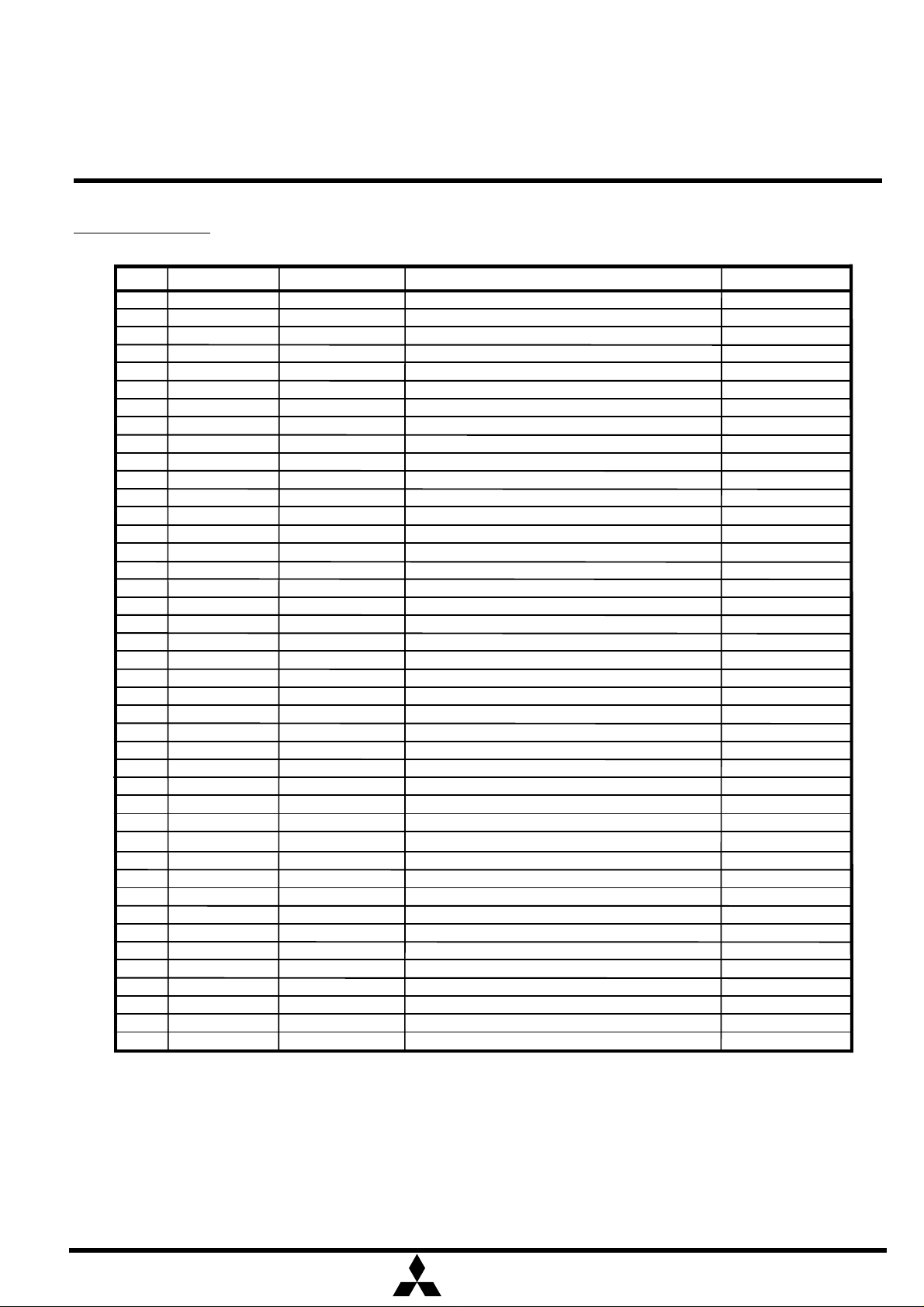
Internal register information
(preliminary)
address
Reset val.
1/9 ex.
RFF_FIX
AUTO_RFF_FIX
PICTURE-IN-PICTURE
bit
<7>
00h
<6>
<5>
<4>
<3>
<2> BGCS
<1> FREE_RUN
<0>
<7:0> VXA<7:0>
01h
02h <7:0> HXA<7:0> Sub picture horizontal position
<7>
03h
<6:0> CONTRAST<6:0>
<7>
04h
<6:0>
<7>
05h
<6>
<5:0>
<7:6>
06h
<5:4>
<3:0>
<7:6> INPUT_SEL<1:0>
07h
<5:0> BG_START<5:0> Sub picture BGP position setting
<7:4>
08h
<3:0> YDL<3:0> Sub picture Y/C delay adjust
<7:5> BGBY<2:0>
09h
<4:0>
<7> VCHIP_ONLY
0Ah
<6:4>
<3:0>
<7:4>
0Bh
<3:0>
<7>
0Ch
<6>
<5:4>
<3>
<2>
<1:0>
symbol
DISP
SIZE_V
SIZE_H
WEN
BGC
RVS
DECODE Sub picture color decoder reset : [1] reset
KILLER
U_DAC<6:0>
GRC
YUVN_RGB_SEL
TINT<5:0>
EXT_SC_SEL<1:0>
DCONT<1:0>
HT<3:0>
ADJ<3:0>
Y_OFFSET<4:0> Sub picture Y bright control
BGRY<2:0> Back ground V level setting
BGY<3:0> Back ground Y level setting
PEDESTV<3:0>
PEDESTU<3:0>
UV_FILTER_OFF
SET_ACC
SYSTEM_MODE<1:0> System : [0]NTSC , [1]PAL-M, [2]PAL-N, [3] N.A.
SET_SIZE
SET_VCHIP
SYNC_DELAY<1:0>
0
0
0
0
0
0
0
0 0
0
0 0
00h
0h 0h
0 0
0h 0h
0
0h
0h
0h
0
0
0h
0
0
0
1
Sub picture display : [0] off, [1] on
0
Sub picture vertical size : [0] 1/9, [1] 1/16
0
Sub picture horizontal size : [0] 1/9, [1] 1/16
1
Sub picture : [0] Still, [1] Moving
0
Back ground display : [0] off, [1] on
0
Sub picture mute : [0] off, [1] on
0
VCXO oscilation : [0] Lock, [1] Free run
HD/VD input synchronous mode selection : [0] sync., [1] async.
0
Sub picture vertical position
20h
20h
Sub picture Y or R DAC output amplitude control
32h
0
Sub picture color killer : [0] enable, [1] disable
Sub picture U or G DAC output amplitude control
32h
Frame display : [0] off, [1] on
1
PIP output mode selection : [0] YUV, [1] RGB
00h
Sub picture tint control
Sub picture C-Sync sep. input selection :
[0] Digital, [1] int. Auto slice [2] external (18 pin), [3] Int. analog
Sub picture sync sep.threshold setting (analog/digital)
Ah
Sub picture display timing adjust
Sub picture input selection : [0] YC, [1] N.A., [2]CVBS, [3] YUV
2h
0Eh
Main/Sub switch delay control
2h
5h
Back ground U level setting
0Fh
0
V-chip decode mode : [0] off, [1] on
0h
Ch
0h
Sub picture V pedestal level (2's comp)
Sub picture U pedestal level (2's comp)
0h
Sub picture U, V output filter : [0]on, [1]off
0
0
Address 0Dh, 0Eh setting mode : [0]default, [1] enable to set
0h
0
Address 11h - 14h setting mode : [0]default, [1] enable to set
Address 15h - 17h setting mode : [0]default , [1] enable to set
0
Sub picture sync.delay control
0
remarks
<7:4>
0Dh
<3>
<2> WDOF_KILLER_ON
<1>
<0> CVF
<7>
0Eh
<6>
<5:0>
<7>
0Fh
<6>
<5>
<4>
<3>
<2> VMODE
<1>
<0>
YUV_COL<3:0>
C_GAIN_SEL Sub picture chroma : [0] x1, [1] x2
EDGE_RES
BITSEL
AFCBITSEL
ACC_LEVEL<5:0>
AUTO_ENABLE
BURST_CLOCK_MODE
PALN_DISABLE
INV_WFF
INV_RFF
0h
0h
0h
0h
Sub picture color control parameter when YUV input
0h
0
0
0h
Sub picture killer on when its vert. sync lost : [0] on, [1] off
0h
for test : 0 set only
Internal chroma comb filter : [0] on : [1] off
0h
0
0
0
0
0
0
0
0
0
0
Sub picture Y clamp time constant : [0] x2, [1] x1
0
Sub picture AFC time constant : [0] x2, [1] x1
0
Sub picture color decoder amplitude
15h
System automatic judgment : [0] off, [1] on
0
VCXO mode selection : [0] 1H based, [1] 2H based
0
Main picture PAL-N : [0] enable, [1] disable
0
0
Invert sub picture field definition : [0] normal, [1] invert
0
Invert main picture field definition : [0] normal, [1] invert
Vertical display modewhen PAL-N input : [0] normal, [1] wide
0
Main picture field fix : [0] not fix, [1]fix
0
Automatic 50/60Hz Judgment : [0] enable, [1] disable
1
MITSUBISHI
8
ELECTRIC
Page 9

M65665SP/FP
MITSUBISHI DIGITAL TV ICs
SIGNAL PROCESSING
(preliminary)
Test use; Always '1' when 10h<5:4> = "00" (Read only)
Sub picture V sync is : [0] present, [1] not present (Read only)
EDS data flag of even field : [0] no EDS, [1] EDS (Read only)
EDS data flag of odd field : [0] no EDS, [1] EDS (Read only)
Test use (Read only)
Read request of even field : [0] no, [1] requesting (Read only)
Read request of odd field : [0] no, [1] requesting (Read only)
Even field Sliced data upper 8 bit (Read only)
Even field Sliced data lower 8 bit (Read only)
Odd field Sliced data upper 8 bit (Read only)
Odd field Sliced data lower 8 bit (Read only)
Main picture V sync is : [0] present, [1] not present (Read only)
Sub picture vertical sync detection (Read only)
Test use (Read only)
Reset val.
1/9 ex.
address
PICTURE-IN-PICTURE
Internal register information (continuing)
bit
10h
<7:6>
<5:4>
<3:0> PALRY<3:0> Threshold control of ident judgment of sub picture decoder
<7>
11h
<6:0>
12h
<7:0>
<7:2>
13h
<1:0>
<7:6> MVC<1:0>
14h
<5:0> VXS<5:0>
<7>
15h
<6> PLUS
<5>
<4:0> LINE_NUM<4:0>
16h <7:0> STB_DLY<7:0>
17h <7:0>
<7> EDGE_ON
18h
<6:4>
<3:0>
<7:5>
19h
<4>
<3:0> FREE_RUN_ADJ<3:0> Frequency adjustment control when free run mode (2's comp)
<7:0>
1Ah
<7:6>
1Bh
<5>
<4>
<3:0>
<7>
1Ch
<6:0> V_DAC<6:0>
symbol
NO_BST_LEVEL
BW_DET_LEVEL
CROSS_SEL
HYA<6:0>
VYA<7:0> Sub picture vertical display line number
HX<5:0>
HP<1:0>
-
-
L_LEVEL<7:0>
BGBY_EDGE<2:0>
BGY_EDGE<3:0> Frame data independent Y data setting
BGRY_EDGE<2:0> Frame data independent R-Y data setting
HPFOFF Sub picture Y output HPF : [0]on, [1]off
SUB_PALM_JDGE<7:0>
EXPORT<1:0>
INV_UV
AFC_OFF
HADJ<3:0>
PINOE
0
0
00h
0
0h
0h
0
0
0
0
0h
0h
0
0h
0h
0h
0h
0h
0h
0
0h
for test
0
BW det. threshold setting : [0] off, [1] 16mV, [2] 32mV, [3] 64mV
0
00h
Sub picture read mode : [0] pixel based, [1] H based
0
Sub picture horizontal display pixel
37h
44h
1Eh
Sub picture horizontal capture position (coarse)
Sub picture horizontal capture position (fine)
0h
Sub picture C-sync input mask period :
0h
[0] 48us, [1] 44us, [2] 53us, [3] off
Sub picture sample start line
29h
for test : 0 set only
0
for test : 0 set only
0
for test : 0 set only
0
Data slicer line selection
11h
Data slicer start bit detection parameter
40h
Data slicer data slice parameter
82h
Frame data independent control : [0] disable, [1] enable
0
Frame data independent B-Y data setting
0h
0h
0h
0
0h
Parameter setting for PAL-M judgment
0h
Ext. port (7 pin) : [0]"0" output, [1]"1" output [2or3] Sub BGP
0h
0h
Invert U, V output value : [0] normal, [1] invert
Sub picture AFC : [0] on, [1] off
0h
0h
Parameter setting for PAL-M judgment
0
for test
Sub picture V or B DAC output amplitude control
32h
remarks
<7:0>
1Dh
1Eh <7:0>
<7:6> SYSTEM_STATE<1:0>
1Fh
<5>
<4>
<3>
<2>
<1>
<0> WDOF
<7:6>
20h
<5>
<4>
<3>
<2> SIGNAL_OK
<1>
<0> READ_REQA
21h <7:0> PDB<15:8>
22h <7:0> PDB<7:0>
23h <7:0> PDA<15:8>
24h <7:0> PDA<7:0>
PINOE<7:0>
-
MAIN_PALN
SUB_UNLOCK
SUB_PALN
RDOF
MAIN_BW
NOISE<1:0>
- -
WDOF
EDS_ACK2
EDS_ACK1
READ_REQB
for test
E6h
No assignment
Color state : [0] NTSC, [1] PAL-M, [2] PAL-N, [3]N.A.(Read only)
Main is : [0] not PAL-N, [1] PAL-N (Read only)
VCXO is : [0] Lock, [1] Unlock (Read only)
Sub is : [0] not PAL-N, [1] PAL-N (Read only)
MITSUBISHI
ELECTRIC
9
Page 10

M65665SP/FP
MITSUBISHI DIGITAL TV ICs
SIGNAL PROCESSING
PICTURE-IN-PICTURE
The relation of input signal 32-pin (Main-HD) and 33-pin (Main-VD) is shown below
0
32-pin
input
(Main-HD)
33-pin input
(Main-VD)
+10usec-10usec
[Even to Odd]
33-pin input
(Main-VD)
+21.75usec +41.75usec
[Odd to Even]
20us 20us20us20us20us20us
4H 1H
end of vertical equalization pulse
prohibition time of
changing 33-pin signal
+53.5usec
VD input
37.5us
20us
20us 20us 20us
20us 20us
VD input
Driving Method and Operating Specification for Serial Interface Data
(1) Serial data transmission completion and start
A low-to-high transition of the DATA (serial data) line while the CLK (serial clock) is high, that completes the serial transmission and makes the
bus free.
A high-to-low transition of the DATA line while the CLK is high, that starts the serial transmission and waits for the following CLK and DATA
inputs.
(2) Serial data transmission
The data are transmitted in the most significant bit (MSB) first by one-byte unit on the DATA line successively. One-byte data transmission is
completed by 9 clock cycles, the former 8 cycles are for address/data and the latter one is for acknowledge detection. (In reading state, ACK is 'H'
under these two conditions ; 1) the coincidence of two address data for the address data transmission, 2) the completion of 8-bit setting data
transfer. In writing state, ACK is 'H' with the address coincidence and ACK is 'L' for detecting acknowledge input from the master (micro
processor) after sending 8-bit setting data.)
For address/data transmission, DATA must change while CLK is 'L'. (The data change while CLK is 'H' or the simultaneous change of CLK and
DATA, that will be a false operation because of undistinguished condition from the completion/start of serial data transfer).
After the beginning of serial data transmission, the total number of data bytes that can be transferred are not limited.
(3) The byte format of data transmission (The sequence of data transmission)
a. The byte format during data setting to M65665FP are shown as follows.
In right after the forming of serial data transmitting state, the slave address 24h (00100100b) is transferred. Afterwards, the internal register
address (1 byte) and setting data (by 1 byte unit) are transferred successively. Several bytes of setting data can be handled in the one
transmission. In this operation, the setting data are written into the address register whose address is increased one in initially transferred internal
register address.
b. The byte format during data reading from M65665FP are shown as follows.
Before data reading from M65665FP, whose internal address need to be set by the data reading/transmitting. After the data reading/transmitting,
the operation of "serial data transmission completion and start" (described in (1)) is necessary. Continuously, the slave address 25h (00100101b)
is sent, and then the inverted read out data are available on ACK. Several bytes of writing data can be handled in the one transmission, too. In this
operation, the setting data also are written into the address register whose address is increased one in initially transferred internal register address.
MITSUBISHI
ELECTRIC
10
Page 11

M65665SP/FP
MITSUBISHI DIGITAL TV ICs
SIGNAL PROCESSING
PICTURE-IN-PICTURE
<The examples of serial byte transmission format>
(1) The writing operation of the setting data (AAh) into M65665FP internal address of 00h
Transmission
Activation
Confirmation
of bus free
(DATA='H')
yes
S 24h A 00h A AAh A D E
no
is applied
on CLk for the
release of
output state
S : Operation of serial transmission start
A : Acknowledge detection
D : Dummy clock feed for the release of
acknowledge output state
E : Operation of serial transmission completion
(2) The writing operation of the setting data (FFh, 80h, EEh) into M65665FP internal address
of 04h ~ 06h
Transmission
Activation
Confirmation
of bus free
(DATA='H')
yes
S 24h A 04h A FFh AD E80hA A EEh
no
is applied
on CLk for the
release of
output state
(3) The reading operation of the setting data from M65665FP internal address of 00h
Transmission
Activation
Confirmation
of bus free
(DATA='H')
yes
S 24h A 00h A 25h A
D E S $$h A'
no
is applied
on CLk for the
release of
output state
A' : Bus free operation by the
master (micro processor)
MITSUBISHI
ELECTRIC
11
Page 12

M65665SP/FP
MITSUBISHI DIGITAL TV ICs
SIGNAL PROCESSING
(4 pin)
PICTURE-IN-PICTURE
(4) The reading operation of the setting data from M65665FP internal address of
04h ~ 06h
Transmission
Activation
<Timing Diagram>
SCL
Confirmation
of bus free
(DATA='H')
yes
S 24h A 04h A A"25h AD E S $$h $$h A" $$h A'
no
is applied
on CLk for the
release of
output state
1 2 3 4 5 6 7 8 9 1
A" : Output 'L' operation by the
master (micro processor)
SDA
(3 pin)
SDA (Read data)
(3 pin)
ACK
(2 pin)
ACK (Read data)
(2 pin)
Bit7
(MSB)
Bit7
(MSB)
Bit7
(MSB)
Bit6 Bit5 Bit4 Bit3 Bit2 Bit1 Bit0
(LSB)
Bit6
Bit6
Bit5 Bit4
Bit5 Bit4
Bit3 Bit2 Bit1
Bit3 Bit2 Bit1
Bit0
(LSB)
Bit0
(LSB)
ACK
Detec.
Bit7
(MSB)
Bit7
(MSB)
Bit7
(MSB)
MITSUBISHI
ELECTRIC
12
Page 13

M65665SP/FP
MITSUBISHI DIGITAL TV ICs
SIGNAL PROCESSING
DETAILED DIAGRAM OF PACKAGE OUTLINE
PICTURE-IN-PICTURE
c
22
Lead Material
Alloy 42/Cu Alloy
1
e
–3.8–
– – 5.5
0.51 – –
0.35 0.45 0.55
0.9 1.0 1.3
0.63 0.73 1.03
Min Nom Max
Dimension in Millimeters
2
1
A
Symbol
E
21
b
A
A
A2A1
0.22 0.27 0.34
1
c
b
b2
– 1.778 –
– 15.24 –
0° –15°
36.5 36.7 36.9
12.85 13.0 13.15
E
D
3.0 – –
e
L
e1
b2
b
1
b
4.1
Weight(g)
–
JEDEC Code
SDIP42-P-600-1.78
EIAJ Package Code
42P4B Plastic 42pin 600mil SDIP
42
1
MITSUBISHI
ELECTRIC
D
e
L A
SEATING PLANE
13
Page 14

M65665SP/FP
MITSUBISHI DIGITAL TV ICs
SIGNAL PROCESSING
PICTURE-IN-PICTURE
.42
I2
–
b2
e
Recommended Mount Pad
e1
F
–
Min Nom Max
Dimension in Millimeters
A
Symbol
.50
.20
.717
.150
.130
c
.517
.317
D
2 A1
A
.68–.2312
.48
.28–.6311
E
–
–
.02
.40
–
.350
.050
–
2
b
A
A1
A
.70–.150
.80
.9311
.50
.30
E
e
L
H
.7651
–
1
L
L1
–
–
–
–
y
L
.4311
–
.271
–
–.50–
0°–10°
2
I2
e1
b
c
Detail F
Lead Material
Alloy 42/Cu Alloy
0.63
Weight(g)
–
JEDEC Code
42 22
EIAJ Package Code
SSOP42-P-450-0.80
42P2R-A Plastic 42pin 450mil SSOP
21
b
y
D
1
E
HE
e
MITSUBISHI
ELECTRIC
14
Page 15

M65665SP/FP
MITSUBISHI DIGITAL TV ICs
SIGNAL PROCESSING
PICTURE-IN-PICTURE
Keep safety first in your circuit designs!
lMitsubishi Electric Corporation puts the maximum effort into making semiconductor products better and more
reliable, but there is always the possibility that trouble may occur with them. Trouble with semiconductors may
lead to personal injury, fire or property damage. Remember to give due consideration to safety when making your
circuit designs, with appropriate measures such as (i) placement of substitutive, auxiliary circuits, (ii) use of nonflammable material or (iii) prevention against any malfunction or mishap.
Notes regarding these materials
lThese materials are intended as a reference to assist our customers in the selection of the Mitsubishi
semiconductor product best suited to the customer’s application; they do not convey any license under any
intellectual property rights, or any other rights, belonging to Mitsubishi Electric Corporation or a third party.
lMitsubishi Electric Corporation assumes no responsibility for any damage, or infringement of any third-party’s
rights, originating in the use of any product data, diagrams, charts, programs, algorithms, or circuit application
examples contained in these materials.
lAll information contained in these materials, including product data, diagrams, charts, programs and
algorithms represents information on products at the time of publication of these materials, and are subject to
change by Mitsubishi Electric Corporation without notice due to product improvements or other reasons. It is
therefore recommended that customers contact Mitsubishi Electric Corporation or an authorized Mitsubishi
Semiconductor product distributor for the latest product information before purchasing a product listed herein.
The information described here may contain technical inaccuracies or typographical errors. Mitsubishi Electric
Corporation assumes no responsibility for any damage, liability, or other loss rising from these inaccuracies or
errors.
Please also pay attention to information published by Mitsubishi Electric Corporation by various means,
including the Mitsubishi Semiconductor home page (http://www.mitsubishichips.com).
lWhen using any or all of the information contained in these materials, including product data, diagrams, charts,
programs, and algorithms, please be sure to evaluate all information as a total system before making a final
decision on the applicability of the information and products. Mitsubishi Electric Corporation assumes no
responsibility for any damage, liability or other loss resulting from the information contained herein.
lMitsubishi Electric Corporation semiconductors are not designed or manufactured for use in a device or system
that is used under circumstances in which human life is potentially at stake. Please contact Mitsubishi Electric
Corporation or an authorized Mitsubishi Semiconductor product distributor when considering the use of a
product contained herein for any specific purposes, such as apparatus or systems for transportation, vehicular,
medical, aerospace, nuclear, or undersea repeater use.
lThe prior written approval of Mitsubishi Electric Corporation is necessary to reprint or reproduce in whole or in
part these materials.
lIf these products or technologies are subject to the Japanese export control restrictions, they must be exported
under a license from the Japanese government and cannot be imported into a country other than the approved
destination.
Any diversion or reexport contrary to the export control laws and regulations of Japan and/or the country of
destination is prohibited.
lPlease contact Mitsubishi Electric Corporation or an authorized Mitsubishi Semiconductor product distributor
for further details on these materials or the products contained therein.
MITSUBISHI
ELECTRIC
15
 Loading...