

Page 1
×
×
∗
∗
MITSUBISHI ICs (TV)
M65617SP
PICTURE-IN-PICTURE SIGNAL PROCESSING
DESCRIPTION
This system is an NTSC system PinP system that accommodates
subscreen composite input and main screen Y/C input. It is a
semiconductor IC circuit having a built-in 96K bit field memory and
an analog circuit, which permits a low-cost and compact system
configuration.
FEATURES
•
Built-in field memory 96K bit for PIP
•
Built-in luminance signal vertical filter
•
No. of subscreen displays: 1 (two sizes, 1/9 and 1/16, can be
selected from.)
•
No. of subscreen samples (1/9 - 1/16 sizes)
No. of quantization bits: 6 for all Y, B-Y and R-Y
No. of horizontal picture elements: 171(Y), 28.5 (B-Y, R-Y)
No. of vertical lines: 69/52
Subscreen frame display ON/OFF
•
Built-in analog circuits such as sync chip clamp, VCXO, and ana-
•
log switch
Built-in 2 channels of 8 bit A/D converter
•
(for main signal burst lock and PIP sub signal)
Built-in two channels of 8 bit D/A converter (luminance and
•
chroma signals)
2
•
I
C bus control
Controls: display ON/OFF, display size selection, setting of
display position, frame ON/OFF, setting of frame level, selection
of frame animation/field still image, setting of Y delay amount,
color level, tint, black level, etc.
APPLICATION
TV
RECOMMENDED OPERATING CONDITION
Supply voltage range........................................................3.1 to 3.5V
Operating frequency.........................................................14.32 MHz
Operating temperature....................................................-10 to 75 ° C
Input voltage (CMOS interface)"H"........................V
DD
"L".............................0 to V
Output current (output buffer)........................................ ± 4mA (MAX)
Output load capacitance............................................20pF (MAX)
Circuit current.........................................................................140mA
0.7 to V
DD
DD
0.3V
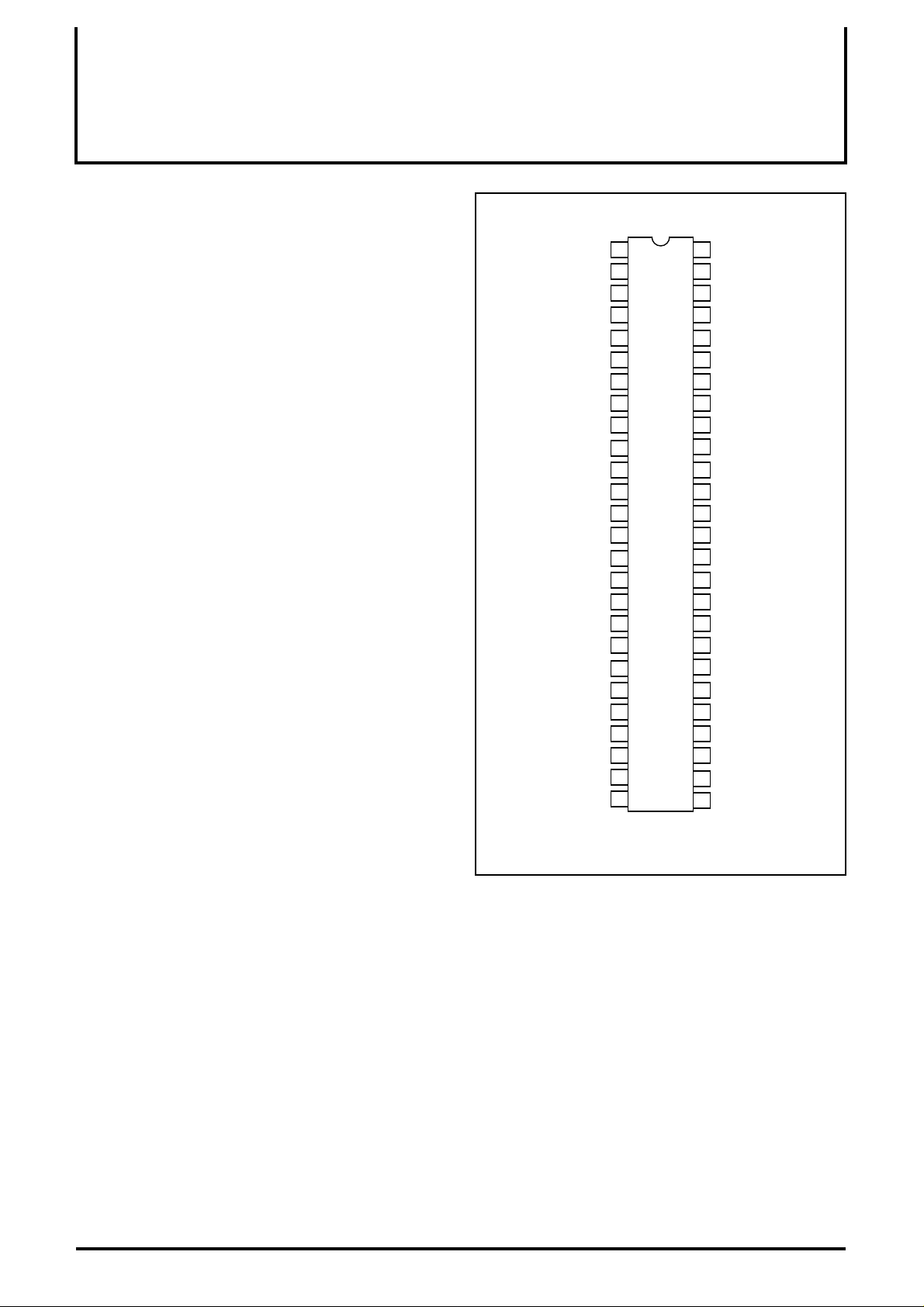
PIN CONFIGURATION (TOP VIEW)
AVss3 (vcxo)
VCXO out
VCXO in
FILTER
AVdd3 (vcxo)
AVdd2 (m)
Vin (m)
Vrt (m)
Vrb (m)
AVss2 (m)
AVdd1 (s)
Vrb (s)
AVss1 (s)
RESET
DVdd1
BGP(s)/TEST0
CSYNC(s)/TEST1
V
1
BIAS
Vin (s)
Vrt (s)
DVss1
SCK
ACK
DATA
CLK
DVss2
1
2
3
4
5
6
7
8
9
10
11
12
13
14
15
16
17
18
19
20
21
22
23
24
25
26
Outline 52P4B
52
51
50
49
48
47
46
45
44
43
42
M65617SP
41
40
39
38
37
36
35
34
33
32
31
30
29
28
27
AVssf (ana)
Cin
TESTEN
Yin
TEST9
Y-PIP
TEST8
C-PIP
AVdd4 (da)
C-PIPin
AVss4 (da)
Y-PIPin
ADJ-Ysub
Yout-sub
ADJ-Csub
Cout-sub
DVss3 (ram)
DVdd3 (ram)
SWMG/TEST7
VD/CSYNC/TEST6
HD/TEST5
SWM/TEST4
MCK
fsc/TEST3
BGP(m)/TEST2
DVdd2
NOTICE: Connect a 0.1 µ F or larger capacitor between V
pins.
1 : Include pin capacitance (7pF)
1
DD
and V
SS
Page 2
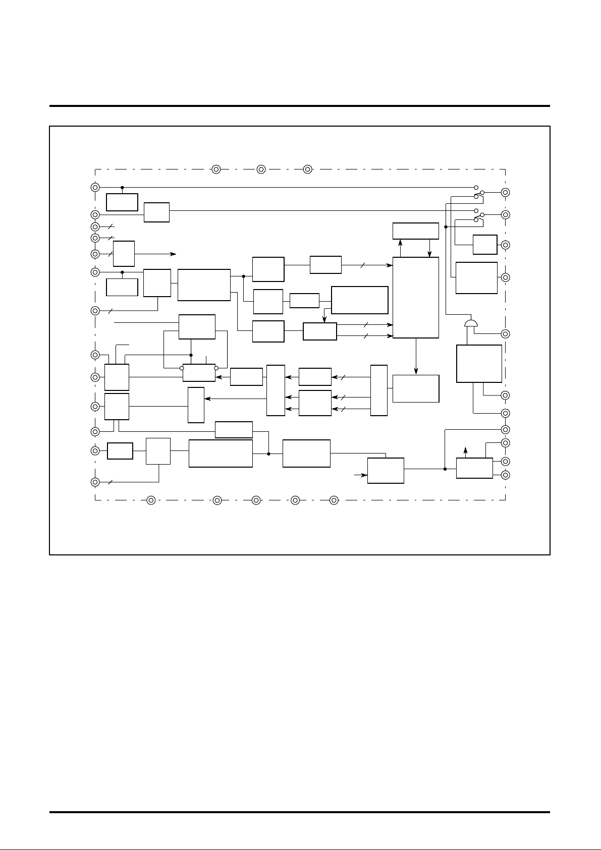
BLOCK DIAGRAM
MITSUBISHI ICs (TV)
M65617SP
PICTURE-IN-PICTURE SIGNAL PROCESSING
SCK
CSYNC(s)
/TEST1
BGP(s)
/TEST0
Yin
Cin
Vdd / Vss
for test
DATA
CLK
ACK
Vin(s)
Vrt(m)
Vrb(m)
ADJ-Ysub
Yout-sub
Cout-sub
ADJ-Csub
Vin(m)
Vrt(m)
Vrb(m)
15
3
3
2
HD
2
Sync tip
Clamp
I2C
I/F
Sync tip
Clamp
D/A
8bit
D/A
8bit
Bias
Y- PIP
Bias
RAM(1H)
Bias
C
Y6
Timing Gen
(Decode)
B-Y
R-Y
6Y
B-Y
6
R-Y
6
6
6
Demux
VCXO
Driver
Vert-filter
&
MUX
Y
B-Y
R-Y
RAM
96Kbits
Back Porch
Clamp
Timing Gen
(Memory
Cont)
4fsc
VCXO
Luma
Y
C
Delay
Clamp
Sync
Sep
Demod
MIX
A/D
8bit
2
C )
( I
A/D
8bit
HPLL
Y/C SEP
(LPF,BPF)
Phase
Select
4fsc
Delay
fsc
Encode
Burst Data
Sampling
Level
Detect
Delay
AFC
Tint
Delay
LPF
&MPY
Phase
Detect
Lock/Free-run
via I
2
C- PIP
C- PIPin
Y- PIPin
SWMG
/TEST7
VD
/CSYNC
/TEST6
HD
/TEST5
FILTER
BIAS
VCXO in
VCXO out
RESET
MCK
BGP(m)
/TEST2
fsc
/TEST3
SWM
/TEST4
2
Page 3
MITSUBISHI ICs (TV)
M65617SP
PICTURE-IN-PICTURE SIGNAL PROCESSING
DESCRIPTION OF PIN
Pin No. Name I/O Function Remarks
1 AVss3
(VCXO)
2 VCXO out O Oscillation output signal
3 VCXO in I Oscillation input signal
4 FILTER O Filter
5 BIAS O Bias
6 AVdd3
(VCXO)
7 AVdd2 (m) Vdd Power supply (analog main signal A/D section)
8 Vin (m) I Main color input signal
9 Vrt (m) O Main signal A/D reference voltage output +
10 Vrb (m) O Main signal A/D reference voltage output 11 AVss2 (m) GND Grounding (analog main signal A/D section)
12 AVdd1 (s) Vdd Power supply (analog sub-signal A/D section)
13 Vin (s) I Sub-composite video input signal
14 Vrt (s) O Sub-signal A/D reference voltage output +
15 Vrb (s) O Sub-signal A/D reference voltage output 16 AVss1 (s) GND Grounding (analog sub-signal A/D section)
17 RESET I Power-ON reset input signal.
18 DVss1 GND Grounding (digital section)
19 DVdd1 Vdd Power supply (digital section)
BGP(s)/TEST0
20
21 SCK I Sub-screen 4fsc clock input Grounding
CSYNC(s)/TEST1
22
23 ACK O
24 DATA I
25 CLK I
26 DVss2 GND Grounding (digital section)
27 DVdd2 Vdd Power supply (digital section)
BGP(m)/TEST2
28
29 fsc/TEST3 I(/O) For testing Pulldown 15k Ω
30 MCK I For testing Grounding
31 SWM/TEST4 (I/)O For testing Open
32 HD/TEST5 I(/O) Horizontal sync input signal
VD/CSYNC/
33
TEST6
SWMG/TEST7
34
35 DVdd3 (ram) Vdd Power supply (digital RAM section)
36 DVss3 (ram) GND Grounding (digital RAM section)
37 Cout-sub O Sub-screen color signal D/A output signal
38 ADJ-Csub O For adjustment of sub-screen color signal D/A
39 Yout-sub O Sub-screen luminance signal D/A output signal
40 ADJ-Ysub O For adjustment of sub-screen luminance signal D/A
41 Y-PIPin I Sub-screen luminance signal re-input signal
42 AVss4 (da) GND Grounding (analog D/A and SW sections)
43 C-PIPin I Sub-screen color signal re-input signal
44 AVdd4 (da) Vdd Power supply (analog D/A & SW sections)
45 C-PIP O PIP color signal output signal
46 TEST8 I For testing Pullup 15k Ω
47 Y-PIP O PIP luminance signal output signal
48 TEST9 I For testing Grounding
49 Yin I Main luminance input signal
50 TESTEN I For testing Grounding
51 Cin I Main color input signal
52 AVssf (ana) Vss Grounding (analog section)
GND Grounding (analog burst lock PLL section)
Vdd Power supply (analog burst lock PLL section)
Connected to the power supply with
100k Ω , and grounded with 10 µ F
(I/)O Sub-screen burst gate pulse output Open
I(/O) Sub-screen CSYNC input Pulldown 15k Ω
2
I
C bus data/acknowledge output signal
2
I
C bus data input signal
2
I
C bus clock input signal
(I/)O For testing Open
I(/O) Vertical sync input signal
I(/O) Sub-screen display authorization input signal Pullup 15k Ω
3
Page 4
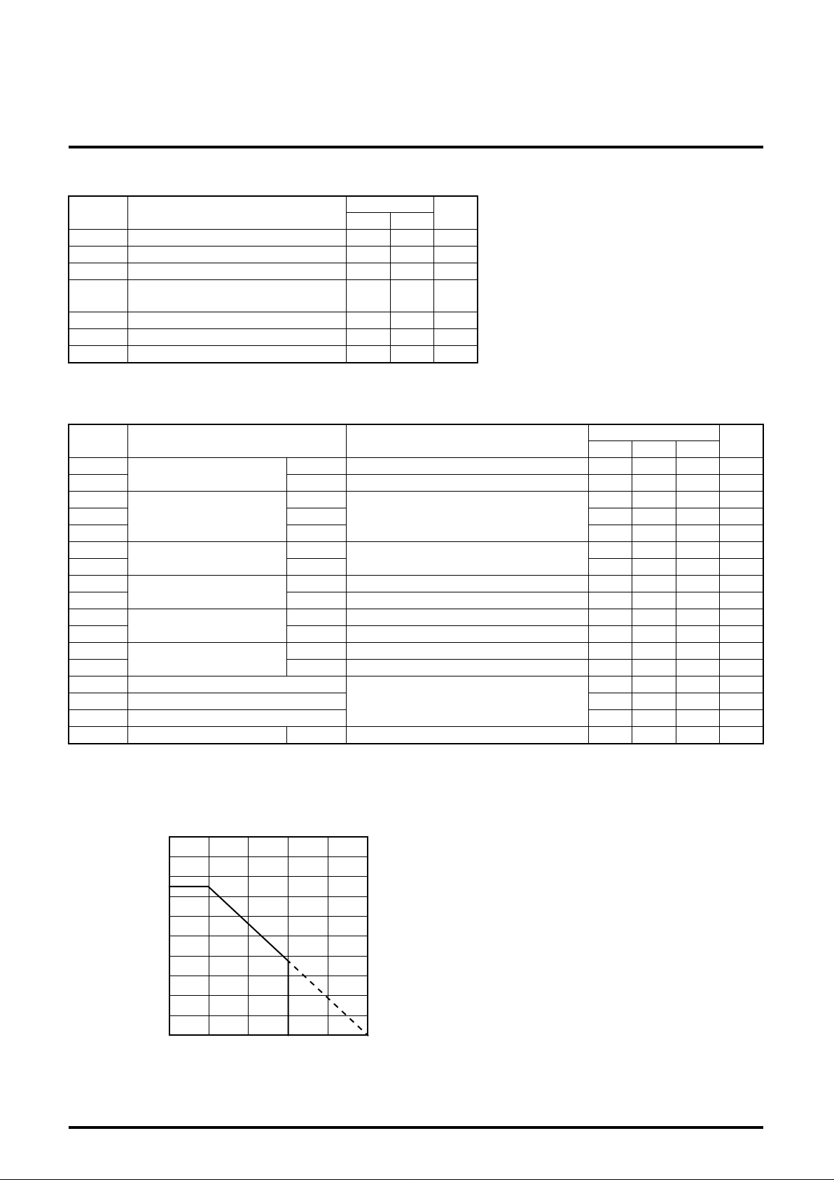
ABSOLUTE MAXIMUM RATINGS
Symbol Parameter
V
DD3
V
I
V
O
O
I
P
d
T
opr
T
stg
1: Output current per output terminal. But P
Supply voltage (3.3V) -0.3 4.6 V
Input voltage -0.3
Output voltage -0.3
Output current
1)
Power dissipation
Operating temperature -10 75 ° C
Storage temperature -50 125 ° C
d
limits all current.
(V
SS
=0V)
∗
Limits
Min. Max.
−
−
V
+0.3
DD3
V
+0.3
DD3
OL
I
=20
I
OH
=-26
1400 mW
( ∗
−
−
−
−
−
−
|
−
MITSUBISHI ICs (TV)
M65617SP
PICTURE-IN-PICTURE SIGNAL PROCESSING
Unit
V
V
mA
−
−
−
−
−
−
SS
(V
DC ELECTRICAL CHARACTERISTICS
=0V)
Symbol Parameter Test conditions
V
IL
V
IH
V
T
-
V
T
+ + 1.4
V
H
V
OL
V
OH
I
OL
I
OH
I
IH
I
IL
I
OZL
I
OZH
C
I
C
O
C
IO
I
DD
Input voltage
(CMOS interface)
Input voltage schmitt trigger
(CMOS interface)
Output voltage
Output current
Input current
Output leakage current
Input pin capacitance
Output pin capacitance
Bidirectional pin capacitance
Operating current
L level V
H level V
DD
=2.7V 0
DD
=3.6V 2.52
–
DD
=3.3V
V
Hysteresis
L level
H level 3.25
L level V
H level V
L level V
H level V
L level V
H level V
3.3V supply
V
DD
=3.3V, | I
DD
=3.0V , V
DD
=3.0V , V
DD
=3.6V , V
DD
=3.6V , V
DD
=3.6V , V
DD
=3.6V , V
f=1MHz, V
O
<1 µ A
OL
=0.4V 4
OH
=2.6V
I
=0V -1
I
=3.6V -1
O
=0V -1
O
=3.6V -1
DD
=0V
TYPICAL CHARACTERISTICS
Limits
Min. Typ. Max.
0.81 V
3.6 V
0.5
1.65 V
2.4 V
0.3
−−
1.2 V
0.05 V
−−
−−
−−
-4 mA
1 µ A
1 µ A
1 µ A
1 µ A
7 15 pF
7 15 pF
7 15 pF
−− 140 mA
Unit
V
mA
THERMAL DERATING (MAXIMUM RATING)
2000
1600
1490
1200
800
400
POWER DISSIPATION Pd (mW)
0
0 25 75 125
50
100
AMBIENT TEMPERATURE Ta (°C)
4
Page 5
PICTURE-IN-PICTURE SIGNAL PROCESSING
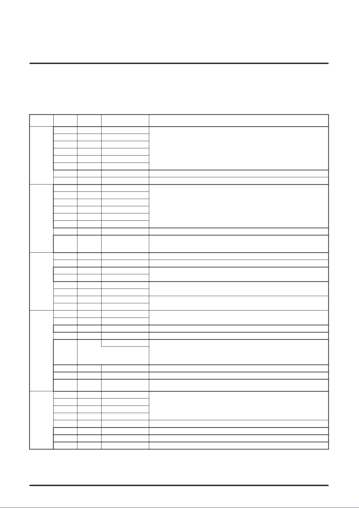
SERIAL REGISTER INFORMATION (device address=24h, sub-address=00h to 0Fh)
Registers requiring user selection/adjustment setting are enclosed in rectangles.
Indication method of reference setting column:Thick letters: Fixed setting value
Standard letters: An example as setting for evaluation
∗/∗: 1/9 - 1/16 sizes
Sub-
address
00h
01h
02h
03h
04h
Bit No.
Reference
setting
0 1 color (0)
1 1 color (1)
2 1 color (2)
3 1 color (3)
4 1 color (4)
5 1 color (5)
6 1 color (6) [1 setting]
7 0 killer Color killer; ON [0], OFF [1], [0 setting]
0 0 tint (0)
1 0 tint (1)
2 0 tint (2)
3 0 tint (3)
4 0 tint (4)
5 0 tint (5)
6 0 afcoff [0 setting]
7 NB decode
0 0 evenupra Setting of interlace leading line; leading field first/second [1/0], [0 setting]
1 0 bgcs Forced writing of background level [1 significant, normally 0] [0 setting]
2 0 extport (0)
3 1 extport (1)
4 0 adclocksel (0)
5 0 adclocksel (1)
6 1 mode (0)
7 0 mode (1)
0 1 crtint (0)
1 1 crtint (1)
2 1/0 size-h Horizontal size
3 0 hpfoff Emphasis of high luminance signal area ON/OFF [0/1] [0 setting]
NB bgpmsel
1 in case of 03h<7>(rvs)=1 or
4
03h<6>(rvhs)=1,
0 in other cases
5 0/1 size Vertical size
6 0 rvhs Addition of sync, burst; OFF/ON [0/1] [Normally 0 setting when PIP is displayed]
70rvs
0 0 ydl (0)
1 0 ydl (1)
2 1 ydl (2)
3 0 ydl (3)
4 0 test acc lvl acc reference level setting authorization; [1 significant] [0 setting]
5 1 wen Display of field still screen/display of animation [0/1]
6 1 grc Display of sub-screen frame; NO/YES [0/1]
7 NB stnby=testreset [0] setting (memory access not operated by [1])
Register name Function
Color saturation adjustment; min. value [0], max. value[63], 1/step [3Fh setting]
Tint adjustment; setting by complements of 2
0fl to -50fl [00h to 1Fh]
+50fl to 0fl [20h to 3Fh]
[Normally 00h setting]
Initialization of sub-screen color demodulation; normally [0], initialized [1]
Each time reset is cleared and sub-screen input source changed, operate in a
sequence of 0 - 1 - 0.
2
C bus expansion port data (optional function); [Set to either of them]
I
Selection of adc clock delay; [00b setting]
Selection of IC operation mode; [01b setting] 16 bits [0]
Setting of sub-screen tint offset; [11b setting]
Selection of PIP-Y output clamping pulse; [0 setting when PIP is displayed]
Sync operation; Main input is f ollo w ed [0], self-propelled [1] [0 setting when PIP is
displayed]
Setting of sub-screen Y delay amount
(D/A output phase against color signal); [4 setting]
Min. 280ns [0h], center 0ns [4h], max. +770ns [Fh]
MITSUBISHI ICs (TV)
M65617SP
5
Page 6

SERIAL REGISTER INFORMATION (cont.)
Sub-
address
05h
06h
07h
08h
09h
0Ah
Bit No.
Reference
setting
0 1/0 hp (0)
1 1/0 hp (1)
2 1/0 hx (0)
3 0/0 hx (1)
4 0/0 hx (2)
5 1/0 hx (3)
6 1/0 hx (4)
7 0/0 hx (5)
0 0 contrast (0)
1 0 contrast (1)
2 0 contrast (2)
3 0 contrast (3)
4 0 contrast (4)
5 0 contrast (5)
6 1 contrast (6)
7 NB free-run vcxo oscillation control; lock loop/self-propelled oscillation [0/1]
0 0 bgy (2)
1 0 bgy (3)
2 0 bgy (4)
3 1 bgy (5)
4 0 ext-sync-sel (0)
5 0 ext-sync-sel (1)
6 0 lpf-sel (0)
7 1 lpf-sel (1)
0 0 bgby (0)
1 0 bgby (1)
2 1 bgby (2)
3 0 bgry (0)
4 0 bgry (1)
5 1 bgry (2)
6 0 mvc (0)
7 0 mvc (1)
0 1 bstby (0)
1 1 bstby (1)
2 1 bstby (2)
3 0 bstby (3)
4 1 bstby (4)
5 0 bstby (5)
6 1 bstby (6)
7 0 bstby (7)
0 0/0 vxa (0)
1 0/0 vxa (1)
2 0/0 vxa (2)
3 0/1 vxa (3)
4 0/0 vxa (4)
5 1/1 vxa (5)
6 0/0 vxa (6)
7 0/0 vxa (7)
Register name Function
MITSUBISHI ICs (TV)
M65617SP
PICTURE-IN-PICTURE SIGNAL PROCESSING
Sample start position
Fine adjustment; 70ns/step
Sample start position
Rough adjustment;
Formula: {4-hp<1:0>+(3Fh-hx<5:0>)×4}×70ns-2.5us
Luminance signal sub-DAC control;
1V output at 40h, max. 1.8V output
1V output from sync chip to white peak at 40h
Luminance signal level during image period is 100/130 (IRE ratio) x 1V
[40h setting with evaluation board]
Setting of frame and background luminance level; [8h setting in the case of black
frame]
Selection of sub-screen sync input; [Normally 0 setting]
Digital [0 or 1], external pin input [2], internal analog [3]
Selection of sub-screen luminance signal band [2 setting]
2.3 [00b], 2.1 [01b], 1.6 [10b], 1.3 [11b]MHz
Setting of background b-y level; 8 gradations
0(min.)→4(center)→7(max.) (4 setting if colorless)
Setting of background r-y level; 8 gradations
0(min.)→4(center)→7(max.) (4 setting if colorless)
Setting of noise mask gate range for sub-signal sync;
48us [0], 44us [1], 53us [2], OFF [3] [0 setting]
Setting of color signal output burst b-y level; 256 gradations
00h(min.)→80h(center)→FFh(max.)
Setting of display start position (vertical); {vxa<7.0>+17 or 16 (1st field)}line
[20h/28h(1/9 - 1/16 sizes) when displayed at the upper left]
6
Page 7

SERIAL REGISTER INFORMATION (cont.)
Sub-
address
0Bh
0Ch
0Dh
0Eh
0Fh
Bit No.
Reference
setting
0 0/1 vya (0)
1 0/1 vya (1)
2 1/0 vya (2)
3 0/0 vya (3)
4 0/1 vya (4)
5 0/1 vya (5)
6 1/0 vya (6)
7 0/0 vya (7)
0 0/0 hxa (0)
1 0/0 hxa (1)
2 0/0 hxa (2)
3 1/0 hxa (3)
4 0/1 hxa (4)
5 0/0 hxa (5)
6 0/0 hxa (6)
7 0/0 hxa (7)
0 0/1 hya (0)
1 0/0 hya (1)
2 0/0 hya (2)
3 1/1 hya (3)
4 1/0 hya (4)
5 1/1 hya (5)
6 1 ext-bhsel (0)
7 1 ext-bhsel (1)
0 0 adj (0)
1 0 adj (1)
2 1 adj (2)
3 0 adj (3)
4 1 hadj (0)
5 1 hadj (1)
6 1 hadj (2)
7 1 hadj (3)
0 1 disp Display control; PIP display OFF/ON [0/1] (ineffective at background)
1 0 bgc Background display control; OFF/ON [0/1]
2 0 dofc
3 1 y-offset (0)
4 1 y-offset (1)
5 1 y-offset (2)
6 1 y-offset (3)
7 0 y-offset (4)
Register name Function
MITSUBISHI ICs (TV)
M65617SP
PICTURE-IN-PICTURE SIGNAL PROCESSING
Setting of display period (vertical);
{vya<7:0>} line
[44h/33h (1/9-1/16 sizes)]
Setting of display start position (horizontal);
{hxa0<7:0>×4×70ns+12.8}us
[08h-10h (1/9-1/6 sizes) when displayed at the upper left]
Setting of display period (horizontal);
{(hya0<5:0>-1)×4×70}us
[38h/29h (1/9 - 1/16 sizes)]
Selection of sync input for burst clock;
HD pin [0 or 1], VD pin [2], internal analog [3] [3 setting]
Adjustment of sub-screen display-starting horizontal position; [4h setting]
70ns/step
Min. 280ns [0h], center 0ns [4h], +770ns [Fh]
Adjustment of supplementary BGP position; [Normally Fh setting]
Parameter to adjust PIP Y output signal clamping position to main Y input signal
pedestal (when 03h<4>(bgpmsel) = 1)
5.6us[0h], 6.6us [Fh] (pulse width: 2.6us) from the front end of horizontal sync
Authorization of addition of sync when missing main source is detected; OFF/
ON [0/1]
Setting of luminance signal output DC offset;
Set pedestal level within a range of 32 digits/256 digits (complements of 2, "-16fl
to +15fl" or "0", provides image data bottom values. It serves fine adjustment of
brightness.)
7
Page 8

PICTURE-IN-PICTURE SIGNAL PROCESSING
SERIAL REGISTER INFORMATION (device address=24h, subaddress=10h to 1Bh)
(Device adress=25h [output], subaddress=1Ch to 1Fh
Indication method of reading column: 0 or 1.... Register with readings
∗.... Register unused
MITSUBISHI ICs (TV)
M65617SP
Sub-
address
10h
11h
12h
13h
14h
Bit No.
Reference
setting
0 0 bg-start (0)
1 1 bg-start (1)
2 1 bg-start (2)
3 1 bg-start (3)
4 0 bg-start (4)
5 0 bg-start (5)
6 1 swap chg, dis output transfer control; default/reversal [0/1], [1 setting]
7 0 set-pd-out For testing [0 setting]
0 0 no-bst-level (0)
1 0 no-bst-level (1)
2 0 bw-level (0)
3 0 bw-level (1)
4 0 ext-mh-sel (0) Selection of main horizontal sync signal input; [normally 0 setting]
5 0 ext-mh-sel (1)
6 0 ext-mv-sel
7 1 pin28osel Selection of 28 pin output; BGPM [0], RDOF [1] [Normally 1 setting]
0 0 color-set (0)
1 0 color-set (1)
2 0 color-set (2)
3 0 color-set (3)
4 0 color-set (4)
5 0 color-set (5)
6 1 color-set (6)
7 NB test-pip-c-dac-ctrl
0 1 bgpx (0)
1 0 bgpx (1)
2 1 bgpx (2)
3 1 bgpx (3)
4 1 bgpx (4)
5 0 bgpx (5)
6 0 test-sel180d For testing [Normally 0 setting]
7 0 ti-sel180d For testing [Normally 0 setting]
0 1 color2 (0)
1 1 color2 (1)
2 1 color2 (2)
3 1 color2 (3)
4 1 color2 (4)
5 1 color2 (5)
6 1 dft-wtg 15h<5:0>, 16h<7:0> register default gate [Normally 1 setting]
7 0 teg-vbrin For testing [0 setting]
Register name Function
Setting of burst gate pulse phase for internal burst lock;
Min.value [0], max.value [63],70ns/step
[0Eh setting]
(4.8us, pulse width 3us from the front end of horizontal sync)
For testing [0 setting]
For testing [0 setting]
HD pin[0 or 1], VD-CSYNC pin[2], internal analog [3]
election of main vertical sync signal input; VD-CSYNC pin/internal analog [0/1]
[Normally 0 setting]
Adjustment of color saturation (main burst tracking in);
Min. value x 0[0], max. value x 2 [127], [1]/step
Output analog voltage value depends upon input burst signal level
[Normally 40h setting]
Main burst level tracking function control; ON [0], OFF [1] [0 setting at PIP]
When there is no main input burst signal at background display, set 1 to clear the
main burst tracking function.
Adjustment of burst gate pulse output phase for sub-screen;
[Normal setting value 1Dh]
Adjustment of color saturation; min.v alue [0], max.value [63], 1/step [Normally 3Fh
setting]
8
Page 9

SERIAL REGISTER INFORMATION (cont.)
Sub-
address
15h
16h
17h
18h
19h
1Ah
Bit No.
Reference
setting
0 1/1 vxs (0)
1 0/1 vxs (1)
2 0/0 vxs (2)
3 1/1 vxs (3)
4 0/0 vxs (4)
5 1/1 vxs (5)
6 0 whms For testing [0 setting]
7 0 test-whv For testing [0 setting]
0 0 clr-mod (0)
1 0 clr-mod (1)
2 0 clr-mod (2)
3 0 clr-mod (3)
4 0 clr-mod (4)
5 0 clr-mod (5)
6 0 clr-mod (6)
7 0 clr-mod (7)
0 1 acc-level (0)
1 0 acc-level (1)
2 1 acc-level (2)
3 0 acc-level (3)
4 1 acc-level (4)
5 0 acc-level (5)
6 0 test-clamp For testing; [0 setting]
7 0 autosel For testing; [0 setting]
0 0 doutsel (0)
1 0 doutsel (1)
2 0 clocksis (0)
3 0 clocksis (1)
4 0 cdaoutsel For testing; [0 setting]
5 0 testyt For testing; [0 setting]
6 0 os For testing; [0 setting]
7 0 test-disp For testing; [0 setting]
0 1 dstry (0)
1 1 dstry (1)
2 1 dstry (2)
3 1 dstry (3)
4 1 dstry (4)
5 1 dstry (5)
6 1 dstry (6)
7 0 dstry (7)
0 1 sync (0)
1 1 sync (1)
2 0 bpfsel (0)
3 0 bpfsel (1)
4 1 ht (0)
5 1 ht (1)
6 1 ht (2)
7 0 ht (3)
Register name Function
MITSUBISHI ICs (TV)
M65617SP
PICTURE-IN-PICTURE SIGNAL PROCESSING
Setting of sub-screen sample start position (vertical):
No setting is necessary when 14h<6> is set to "0".
Adjustment setting value is effective when 14h<6> is set to "1".
[29h/2Bh (1/9 - 1/16 sizes)]
For testing [00h setting]
acc reference level: no setting is necessary when 04h<4>=0
[15h setting]
For testing; [00b setting]
Test clock selection; [00b setting]
Setting of color signal output burst r-y level; 256 gradations
00h (min.)→80h (center)→FFh (max.)
Selection of main internal sync separation threshold level; [11b setting]
Selection of BPF function before encoding; [00b setting]
Display information output timing cycle-adjusting parameter;
Adjustment of horizontal display effective data-starting cycle inside ICs
[7h setting]
9
Page 10

SERIAL REGISTER INFORMATION (cont.)
Sub-
address
1Bh
1Ch
read
1Dh
read
1Eh
read
1Fh
read
Bit No.
Reference
setting
0 1 dft-bl Register 10h<7:0>, 11h<3.0>default gate; [1 setting]
1 1 dft-misc Register 11h<7:4>default gate; [1 setting]
2 1 dft-sg Register 13h<7:0>, 14h<6>, 17h<7:6>default gate; [1 setting]
3 1 dft-syncbst Register 19h<7:0>default gate; [1 setting]
4 1 dft-clevel Register 12h<7:0>default gate; [1 setting]
5 0 pin29osel
6 0 pin29oe
7 1 dft-clr Register 16h<7:0>default gate; [1 setting]
0 ∗ imag (0)
1 ∗ imag (1)
2 ∗ imag (2)
3 ∗ imag (3)
4 ∗ iphase (0)
5 ∗ iphase (1)
6 ∗ iphase (2)
7 ∗ iphase (3)
0 ∗ iphase (4)
1 ∗ iphase (5)
2 ∗ iphase (6)
3 ∗ iphase (7)
4 ∗ iphase (8)
5 ∗ for test
6 ∗ for test
7 0 or 1 rdof Simplified verification of main input loss; input unavailable/available [1/0]
0 0 or 1 clamp-offset (0)
1 0 or 1 clamp-offset (1)
2 0 or 1 clamp-offset (2)
3 0 or 1 clamp-offset (3)
4 0 or 1 clamp-offset (4)
5 0 or 1 clamp-offset (5)
6 ∗ for test For testing
7 0 or 1 wdof Simplified verification of sub-input loss; input unavailable/available [1/0]
0 0 or 1 c-dac-ctrl (0)
1 0 or 1 c-dac-ctrl (1)
2 0 or 1 c-dac-ctrl (2)
3 0 or 1 c-dac-ctrl (3)
4 0 or 1 c-dac-ctrl (4)
5 0 or 1 c-dac-ctrl (5)
6 0 or 1 c-dac-ctrl (6)
7 ∗ bw Unlock information; for verification of internal operation information
Register name Function
MITSUBISHI ICs (TV)
M65617SP
PICTURE-IN-PICTURE SIGNAL PROCESSING
Signal selection at 29 pin output mode; fsc/4fsc [0/1] [0 setting]
Operated when adjusting oscillation frequency
29 pin output mode authorization input/output [0/1] [Normally 0 setting]
Operated when adjusting oscillation frequency
For testing
For testing
For testing
Clamping level information; for verification of internal operation information
Values are shown that are in proportion and corresponding to the depth of sub-
input information sync.
Level tracking information; for verification of internal operation information
Values are shown that are in proportion and corresponding to main input burst
amplitude
10
Page 11

APPLICATION EXAMPLE
MITSUBISHI ICs (TV)
M65617SP
PICTURE-IN-PICTURE SIGNAL PROCESSING
Ana.
Dig5V
Digital +5V
power supply
Dig
Digital +3.3V
power supply
Digital GND
Ana.
Analog +3.3V
power supply
Analog GND
Ana.5V
Analog +5V
power supply
Composite video
input signal
(sub-picture)
68p
PIP Luma signal output
Luma signal input (main-picture)
Chroma input signal (main-picture)
104104
PIP Chroma signal output
Ana.
10µ
103
Ana.
15k
104
150p
104
Ana.
103
360
103
470
Vertical sync input signal (main-picture)
Horizontal sync input signal (main-picture)
Sub-picture displaying on/off
Dig
10µ
103
M65617SP
1 26
10p
X1
12p
2.2µ
300
154
1.5µ
103
5101520
820k
CX
10µ
103
103
100k
2k
224
Ana.
Y
C
104
Ana.
SYNC SEP
CIRCUIT
(OPTIONAL)
103
10µ
103
103
Ana.
104
10µ
103
103103
100k
10µ
Dig
330
560
3035404550
Dig5V
47k
100
15k
100
Dig
12k
103
10µ
2752
Dig5V
47k
12k
10k
100
SDA
10k
SCL
2
C BUS Clock
I
input signal
I2C BUS DATA
input/output
signal
11
Separate Y/C signals by using LC-tank circuit or LPF,BPF for Y/C signals level adjust.
And then mix both signals for sub-picture input video signal.
(The above external circuit processing aims at controlling white compression of
sub-screen input luminance signal and strengthening the color playback function of
sub-screen input signal in the case of weak electric field.)
Units Resistance : Ω
Capacitance : F
Page 12

PIP TV SYSTEM BLOCK DIAGRAM
(BASIC)
MITSUBISHI ICs (TV)
M65617SP
PICTURE-IN-PICTURE SIGNAL PROCESSING
Composite
Video Signal
Y/C Separated
Video Signal
Y/C
Separation
Y
C
Y
C
Y
C
CV
(Driving Method and Operating Specification for
Serial Interface Data)
(1) Completion and start of serial transfer
If DATA (serial signal data) is changed from 'L' to 'H' when CLK
(serial clock signal) is 'H', serial transfer is completed to
generate a bus-free status.
If DATA is changed from 'H' to 'L' when CLK is 'H', serial transf er
is started to stand by for subsequent input of CLK and DATA.
(2) Serial data transfer
Data, which is transferred in the unit of 1 byte, is sent
sequentially from the MSB-side bit through DATA. Clock
waveform necessary for the transfer of 1 byte represents 9
times, of which address/data are transferred with the initial 8
times, and acknowledge detection performed with the remaining
one time. (When reading, 'H' is output to ACK at the agreement
of address in the case of address transfer , and at the completion
of the 8 bit portion in the case of setting data transfer. When
writing, 'H' is output to ACK at the agreement of address in the
case of address transfer, and 'L' is output to ACK to detect
acknowledge input from master after 8 bit data is output.)
DATA needs to be changed when CLK is 'L' if address/data is to
be transferred. (Allowing DATA to be changed when CLK is 'H'
or simultaneously with the change of CLK, will cause
maloperation since no identification is possible of the
completion and start of serial transfer.
There are no restrictions on the number of bytes of data
transferred after the start of serial transfer.
M65617SP
BLPLL
B-LD
PIP Signal
Processing
Y
C
Y
C
Video
Signal
Processing
Deflection
Unit
HD VD
Yoke
(3) Data transfer byte format (data transfer sequence)
1. Data transfer byte format in setting data to M65617SP will be
described:
Generate a serial transfer start status before sending slave
address 24h (00100100b), and then send internal register
address (1 byte) followed by setting data (in the unit of 1
byte). For setting data, a single transfer allows more than 1
byte to be transferred. In this case, setting data is read into
the register that has been address-incremented one by one
from the internal register address sent first. (However,
address 00h will be returned to, following address 7Fh.)
2. Data transfer byte format in writing data from M65617SP will
be described:
Prior to writing data, it is necessary to set the internal
address of M65617SP by reading and transferring data. Read
and transfer data before perf orming the completion → start of
serial transfer. Send slave address 25h (00100101b) in
succession, and the reversed information of writing data is
output to ACK thereafter. More than 1 byte of writing data can
also be transferred. In this case as well, setting data is read
into the register that has been address-incremented one by
one from the internal register address sent first. (However,
address 00h will be returned to, following address 7FNn.)
12
Page 13

(The examples of serial byte transmission format)
(1) Reading setting data AAh into internal address 00h of M65617SP:
MITSUBISHI ICs (TV)
M65617SP
PICTURE-IN-PICTURE SIGNAL PROCESSING
Transmission
Activation
Confirmation
of bus free?
(DATA='H')
no
is applied
on CLK for the
release of
output state
yes
S 24h A 00h A AAh A D E
S : Operation of serial transmission start
A : Acknowledge detection
D : Dummy clock feed for the release of
acknowledge output state
E : Operation of serial transmission completion
(2) Reading setting data FFh, 80h and EEh, individually, into internal address 04h to 06h of M65617SP:
Transmission
Activation
Confirmation
of bus free?
(DATA='H')
no
is applied
on CLK for the
release of
output state
yes
S 24h A 04h A FFh
A 80h A EEh
ADE
(3) Writing data on internal address 00h of M65617SP [Standard reading sequence version: 46 pin " L " ]:
Transmission
Activation
Confirmation
of bus free?
(DATA='H')
no
is applied
on CLK for the
release of
output state
yes
S 24h A 00h A
A’ : Bus free operation by the
master (micro processor)
DES
25h A $$h
13
A’
Page 14

MITSUBISHI ICs (TV)
PICTURE-IN-PICTURE SIGNAL PROCESSING
(4) Writing data on internal address 04h to 06h of M65617SP [Standard reading sequence version: 46 pin " H "]:
M65617SP
Transmission
Activation
Confirmation
of bus free?
(DATA='H')
no
is applied
on CLK for the
release of
output state
yes
S 24h A 04h A
A’’ : Output ‘L’ operation by the
master (micro processor)
DES
25h A SSh
(5) Writing data on internal address 00h of M65617SP [Expanded reading sequence version: 46 pin " H"]:
Transmission
Activation
Confirmation
of bus free?
(DATA='H')
no
is applied
on CLK for the
release of
output state
yes
S 25h A 00h A
A’ : Bus free operation by the
master (micro processor)
$$h
A’
A’’
SSh SSh
A’’
A’
(6) Writing data on the internal address 04h to 06h of M65617SP [Expanded reading sequence version: 46 pin " H"]:
Transmission
Activation
Confirmation
of bus free?
(DATA='H')
no
is applied
on CLK for the
release of
output state
yes
S 25h A 04h A
A’’ : Output ‘L’ operation by the
master (micro processor)
SSh
A’’
SSh SSh
A’’
A’
14
Page 15

TIMING DIAGRAM
MITSUBISHI ICs (TV)
M65617SP
PICTURE-IN-PICTURE SIGNAL PROCESSING
CLK
DATA
ACK
_ Acknowledge
ACK
_ Readout data
123456
Bit7
(MSB)
Bit7
(MSB)
Bit6 Bit5 Bit4 Bit3 Bit2 Bit1 Bit0
Bit6 Bit5 Bit4
Bit3 Bit2 Bit1
7
891
(LSB)
Bit0
(LSB)
ACK
Detec.
Bit7
(MSB)
Bit7
(MSB)
15
 Loading...