

Page 1
M65533FP
MITSUBISHI Analog ICs
16
3-0
1
4567891011121314151617181920454647484950515253545556575859606162636480252627282930313233343536373839406566676869707172737475767778792122232441424344
3ch 8-bit 80MHz A/D Converters
General Description
The M65533FP is a CMOS 3ch 8-bit 80MHz analog-to-digital converter by sub-ranging
architecture for high speed video processing. It can be realized 80MHz operation by using
2 ADCs in parallel. And it has PLL circuit generate a stable clock locked to sync signal.
It is a type of "AC" connection with internal clamp circuit and variable input range.
Features
• 3ch 8-bit high speed A-D converters
• Maximum conversion rate 80 MSPS(min.)
• Analog input Level 1.0V(Typ) : 0.5 -1.5 V
• Digital input TTL compatible [ Vinth=1.4V ]
• Digital output VoH=0.7XVcc , VoL=0.3XVcc [ Io=4mA ]
• Low power dissipation 700mW [ CL=10pF ]
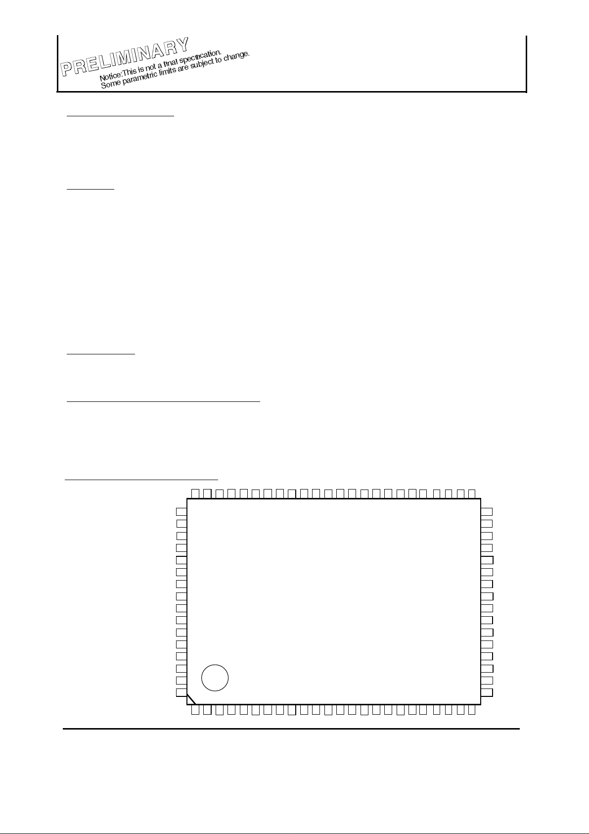
• Package 80 pin QFP package, 0.80mm lead pitch
[ PKG size(without lead) =14mm x 20mm ]
• Small input capacitance 10 pF
• Built-in Reference Voltag Vref(+)=1.5V+150/-330mV(*) Vref(-)=0.5V
• Built-in Clamp circuit Vclamp=0.5V+/-250mV(*)
(*)Controllable by IIC BUS
Applications
• LCD monitor
• High speed video processing
Recommended Operating Condition
• Supply voltage range (typ.=3.3V) 3.15 to 3.45 V
• Supply voltage range (typ.=5.0V) 4.75 to 5.25 V for 5V I/F only
Pin configuration(Top View) Shown on next page
M65533FP
#XXXXXX
Ver 3.0 '99- 5- 31
1 2 3
MITSUBISHI
( / )
Page 2
M65533FP
16
3-0
RCIN
NC
BCIN
NC
GCIN
NC
DVDDG(OUT)
DoR5
Pin Configuration
2
DoR3
DoR2
DoR1
DoR0
DoG6
DoG5
DoG4
DoG3
DoG2
DoG1
DoG0
DoB5
41
DoB6
DoB7
DVDDB(OUT)
DGNDB(OUT)
DoG7
DGNDG(OUT)
DoR4
DoR6
DoR7
DVDDR(OUT)
42
43
44
45
46
47
48
49
50
51
52
53
54
55
56
57
58
59
60
61
62
63
64
3ch 8-bit 80MHz A/D Converters
34353637383940 25272930313233 2628
71706968676665 80787675747372 7977
MITSUBISHI Analog ICs
BNB
24
23
BVRT
22
BVRM
21
AVDDB
20
AGNDB
19
18
17
BVRB
16
GNB
15
GVRT
14
GVRM
13
AVDDG
12
AGNDG
11
10
9
GVRB
8
RNB
7
RVRT
6
RVRM
5
AVDDR
4
AGNDR
3
2
RVRB
1
MITSUBISHI
( / )
Page 3
M65533FP
16
3-0
Block
Diagram
Comparators(2)
1st ADC ( R signal )
CLK-OUT
FILTER
AVDDR
3
IIC BUS
SDA
SCL
EXT-CLK IN
VDD(PLL)
GND(PLL)
SW
DVDD(I/O 5)
DGND(I/O 5)
DVDD(LO)
DGND(LO)
Test1-3
CP-IN
DLY-HDout
DoR0
DoR1
DoR2
DoR3
DoR4
DoR5
DoR6
DoR7
DVDDR(A/D)
MITSUBISHI Analog ICs
3ch 8-bit 80MHz A/D Converters
RC IN
RVRT
RVRM
RVRB
RNB
AGNDR
DGNDR
(A/D)
Comparators(1)
Ladder
Resistors
Comparators(2)
Comparators(1)
Ladder
Resistors
SW
SW
2nd ADC ( G signal )
MUX
&
DeMU
X
MUX
&
DeMU
X
Delay
&
Error
Correctio
n
Delay
&
Error
Correcti
on
DVDDR(out)
DGNDR(out)
Timing
Gen.
3rd ADC ( B signal )
fFBin
FH-IN
fH
PLL
(note) Pins for ADC is described for only R signal
fCLK
MITSUBISHI
RESET
( / )
Page 4
M65533FP
MITSUBISHI Analog ICs
16
3-0
4
---------
-
3ch 8-bit 80MHz A/D Converters
Absolute Maximum Ratings (Ta = 25°C, unless otherwise noted.)
Symbol
DVdd
AVdd
Vdd((I/O) I/O Supply Voltage
VID
IOUT
Pd
Topr Operating Temperature
Tstg
Parameter
Digital Supply Voltage
Analog Supply Voltage
Digital Input Voltage
Analog Output Current
Power Dissipation
Storage Temperature
In current measurement, (+) and (-) is corresponding to an inflow and an outflow current, respectively.
Condition
Ratings
0 to 4.0
0 to 4.0
0 to 6.0
0 to 4.0
-30 to 0
1600
0 to +70
-40 to +150
Unit
V
V
V
V
mA
mW
°C
°C
Recommended Operating Conditions (Ta = 25°C, unless otherwise noted.)
Symbol
Vdd
VIH
VIL
tWH
tWL
tsu
th
Parameter
Supply Voltage
Supply Voltage(I/O)
Digital Input Voltage (High)
Digital Input Voltage (Low)
Clock Pulse Width (High)
Clock Pulse Width (Low)
Set-up Time
Hold Time
Limits
Min. Typ.
3.15
4.75
2.4
6.25
6.25
3.30 3.45
5.0
0 0.8
5
5
Max.
5.25Vdd(I/O)
Vdd
Unit
V
V
V
V
ns
ns
ns
ns
MITSUBISHI
( / )
Page 5
M65533FP
16
3-0
5
8
Electrical Characteristics
(Ta = 25°C, AVdd = DVdd = 3.30V, unless otherwise noted.)
(2) ADC Block
(3) PLL Block
(1) Overall
160
160
MITSUBISHI Analog ICs
3ch 8-bit 80MHz A/D Converters
Symbol
AIdd(AD R/G/B)
DIdd(AD R/G/G)
DIdd(I/O R/G/G)
DIdd(PLL)
DIdd(LO) Logic block Supply Current
DIdd(I/O 5)
AD(R/G/B) Analog Supply Current
AD(R/G/G) Digital Supply Current
I/O block Supply Current
PLL block Supply Current
5V I/O block Supply Current
Parameter
Symbol Parameter
Res
Vdd
NL
DNL
VOH
VOL
VinA
Cin
fCLK
Vref(+)
Vref(M)
Vref(-)
Rref
B.W
tpdLHnsOutput delay time(L->H)
tpdHL
tr
tf
Vclamp
Resolution
Supply Voltage
Integral Nonlinearity
Differential Nonlinearity
Digital output Voltage "H"
Digital output Voltage "L"
Analog input range
Input Capacitance
Max. Conversion Rate
Reference Voltgae "High"
Reference Voltgae "Middle"
Reference Resistor
Input Bandwidth
Output delay time(H->L)
Output rise time
Output fall time
Clamp Voltage
Vref(+)=1.5V, Vref(-)=0.5V
Vref(+)=1.5V, Vref(-)=0.5V
Changeable by IIC (16mV step)
-3dB input frequency
Changeable by IIC (16mV step)
Condition
For R/G/B signal
For R/G/B signal
For R/G/B signal
Condition
Min.
Min.
3.15 3.30
0.7xVdd
0
0.67
80
1.17
0.84
70
0.25
Limits
Typ.
tbf
tbf
tbf
tbf
tbf
tbf
Max.
Limits
Typ. Max.
3.45
± 1.0
± 1.0
Vdd
0.3xVdd
1.00
10
1.5
1.0
0.5
120
110
110
tbf
tbf
0.5
1.15
1.65
1.07
0.73
Unit
mA
mA
mA
mA
mA
mA
Unit
Bits
V
LSB
LSB
V
V
Vp-p
pF
MHz
V
V
VReference Voltgae "Low"
Ohms
MHz
ns
ns
ns
V
Symbol
fH
fVCO
jPLL
D.R(PLL)
Parameter
Horizontal frequency
VCO frequency
maximum jitter
PLL Divider Ratio
from 800 by 1 step
Condition
MITSUBISHI
Limits
Min. Typ.
10
20 80
800
60
0.5
1376
( / )
Max.
100
1.0
Unit
KHz
MHz
ns
-
Page 6

M65533FP
MITSUBISHI Analog ICs
16
3-0
Pin Description -1
It is grounded during actual use.
6
DoX<7:0>
31,33,35
From MCU
I
I/O
Reference Voltage(+) Input (R/G/B signal)
Bypass capacitor
Bypass capacitor
5,13,21
44,54,64
66,67
30,32,34
4,12,20
45,55,65
69,70
2,10,18
7,15,23
6,14,22
1,9,17
8,16,24
46 - 53
74682979788077
25,26,27
36 - 43
56 - 63
3ch 8-bit 80MHz A/D Converters
No connection.
Pin No.
Pin Name
DVDDX(A/D)
AVDDX(A/D)
DVDDX(OUT)
VDD(PLL)
DGNDX (A/D)
AGNDX (A/D)
DGNDX(OUT)
GND(PLL) PLL ground
XVRT
XVRM
I/O
Digital Power supply (R/G/B signal)
Analog Power supply (R/G/B signal)
I/O Power supply (R/G/B signal)
PLL Power supply
Digital ground (R/G/B signal)
Analog ground (R/G/B signal)
I/O ground (R/G/B signal)
R/G/B signal Clamp Input
IXCIN
Reference Voltage(M) Input (R/G/B signal)
Function
From or To
3.3V
3.3V
3.3V
3.3V
GND
GND
GND
GND
From LPF
XVRB
XNB
FH-IN
FILTER
CLK-OUT O
SDA
SCL
RESET
EXT-CLK IN
Test<1-3 > Test terminal
Reference Voltage(-) Input (R/G/B signal)
ADC operating current setting BIAS
O
Digital Output (R/G/B signal)
I
H Sync Input
PLL filter
Clock output
I/O
IIC Data Input/Output
IIC CLK Input
I/O
Reset signal Input
I
External Clock intput
Bypass capacitor
Bypass capacitor
To Logic LSI
From Sync Sep. LSI
(R+C)//C
To Logic LSI
From MCU
To Vdd
From PLL LSI
MITSUBISHI
( / )
Page 7

M65533FP
MITSUBISHI Analog ICs
16
3-0
Pin Description -2
It is grounded during actual use.
7
3.3V
Delayed HD output
From Sync Sep. LSI
7672737175283,11,19
3ch 8-bit 80MHz A/D Converters
No connection.
Pin No.
Pin Name
DVDD(I/O 5)
DVDD (LO)
DGND (I/O 5)
DGND (LO)
CP-IN
DLY-HD out
DLY-HD out
NC
I/O
Digital Power supply (5V)
Digital Power supply (Logic)
Digital ground (5V)
Digital ground (Logic)
Clamp Pulse Input
I
O
Function
From or To
5V
GND
GND
To logic LSI
GND or OPEN
MITSUBISHI
( / )
Page 8

M65533FP
MITSUBISHI Analog ICs
16
3-0
0.504V
0.996V
1.000V
1.496V
1.500V
8
D0="H"
Output "HZ" is available at D1="H" of SubAdd=18h "L"=default
Default
Default
Default
Default
3ch 8-bit 80MHz A/D Converters
Table of Power-down Function( SubAdd=00h, D2-D0) Setting by IIC BUS
Digital input code
"HHH"
"LLL"
Power-down function
power-down
normal operation
Only Clamp=>"HLL"
Only PLL=>"LHL"
Only ADC=>"LLH"
Table of CP Function (SubAdd=11h, D0) Setting by IIC BUS
CP signal
"H"
"L"
CP function
Clamping
Hold state
CP signal
Digital input code
D0="H"
D0="L"
CP Polarity
Inversed
Not-inversed
Table of Hsync Function(SubAdd=17h, D0) Setting by IIC BUS
Digital input code
D0="H"
D0="L"
Hsync function
Inversed
Not-inversed
Table of CLK output Function(SubAdd=13h, D0) Setting by IIC BUS
Digital input code
D0="L"
CLK output function
Inversed (180 )
Not-inversed ( 0 )
Table of Internal/External CLK(SubAdd=16h, D5) Setting by IIC BUS
Digital input code
D5="H"
D5="L"
CLK output function
External
Internal
Table of Digital Output R/G/B < 7 : 0 > Function Setting by IIC BUS
Analog input voltage
0.500V
Digital output code
7
MSB
6
1
1 1 1 1 1 1 1
1 1 1 1 1 1 1 0
1 0 0 0 0 0 0 0
0 1 1 1 1 1 1 1
0 0 0 0 0 0 0 1
0 0 0 0 0 0 0 0
12345
0
LSB
Note
MITSUBISHI
( / )
Page 9

M65533FP
16
3-0
9
Table of Delay adjustment(SubAdd=16h, D3-D0)
5ns
35ns
40ns
70ns
75ns
Setting by IIC BUS
Default
-80LSB
-24LSB
-20LSB
36LSB
40LSB
Setting by IIC BUS
1.5+0.157V
1.5-0.329V
for External CLK (SubAdd=16h, D5="H")
Digital input code
CLK Delayed Adjustment
D0
D3
D2
D1
MITSUBISHI Analog ICs
3ch 8-bit 80MHz A/D Converters
1
1
1
1
0
0
0
1
1
1
0
0
1
1
0
0
0
0
1
0
0
1
1
0
0ns
Table of Vref(+) Voltage adjustment
(SubAdd=0Bh, D4-D0:R 0Ch, D4-D0:G 0Dh, D4-D0:B)
Digital input code
D4 D2 D1 D0
D3
1
1
1
1
1
Vref(+) adjustment
Note
1
1
1
0
0
0
1
0 1 0 1
0
1
0
0
1
0
1
0
0
1
0
0LSB
0
1
0
0
0
1
1
0
-84LSB
MITSUBISHI
1.5-0V
Default
( / )
Page 10

M65533FP
MITSUBISHI Analog ICs
16
3-0
10
(SubAdd=0Eh, D4-D0:R 0Fh, D4-D0:G 10h, D4-D0:B)
-60LSB
-4LSB
0LSB
56LSB
60LSB
Default
0.5V-0mV
0.5V-251mV
CLK output phase
Setting by IIC BUS
3ch 8-bit 80MHz A/D Converters
Table of Clamp level adjustment
Digital input code
D4
1
1
1
0
0
0
D3
1
1
0
1
0
0
D2
1
1
0
1
0
0
D1
D0
1
1
0
1
0
0
Delay adjustment level
1
0
0
1
1
0
-64LSB
0.5V+235mV
Table of CLK output Phase (SubAdd=12h, D4 -D0)
Digital input code
D4 D2 D1 D0
D3
Setting by IIC BUS
Note
1
1
1
1
1
1
1
1
1
0
division into 32
1
0
0
0
0
1
0
0
0
1
0
0
0
1
0
0
0
1
1
0
of 1 period
0 + 0 * 360/32
Default
Table of CLK output Phase Function (SubAdd=12h,D5)
Digital input code
D5="H"
D5="L"
CLK output Phase Function
OFF
ON
Table of CLK's Pol. for A/D (SubAdd=12h,D6)
Digital input code
D6="H"
D6="L"
CLK's Pol.
NEGA
POSI
Setting by IIC BUS
Setting by IIC BUS
MITSUBISHI
( / )
Page 11

M65533FP
MITSUBISHI Analog ICs
16
3-0
11
0
1
1
1
0
0
0
1
1
1
0
0
1
0
0
0
(SubAdd=14h,A6-A0 15h,A3-A0)
3ch 8-bit 80MHz A/D Converters
Table of PLL divider adjustment
Digital input code
14h 15h
A6
1
1
A5
0
0
0
A4
0
0
01 0
1
1
1
A3
1
1
1
1
1
A2
0
0
0
1
0
0
A1
1
1
0
0
1
1
1
Table of PLL divider adjustment
(SubAdd=15h,A6-A5)
A0
1
1
0
0
Setting by IIC BUS
Divider adjustment
A3
0
0
A2
0
1
0
1
0
0
A1
0
1
0
1
0
0
A0
0
fH x 1376
fH x 1375
fH x 1024
fH x 1023
fH x 801
fH x 800
Setting by IIC BUS
1/2
1/3
1/4
1/6
Digital input code
D6,5="1 1"
D6,5="1 0"
D6,5="0 1"
D6,5="0 0"
PLL Pre-divider adjustment
1/6
1/4
1/3
1/2
20 30 40 60 80
O/P Frequency [MHz]
MITSUBISHI
( / )
Page 12

M65533FP
16
3-0
Table of Reset Function (pin 80)
12
Reset signal Reset function
"L"
"H"
Reset
normal operation
MITSUBISHI Analog ICs
3ch 8-bit 80MHz A/D Converters
MITSUBISHI
( / )
Page 13

M65533FP
16
3-0
Application Examples
14
B-in
Vdd=3.3V(typ.)&5V(*)
CP-IN(**)
MCU
PKG:20P2N
MITSUBISHI Analog ICs
3ch 8-bit 80MHz A/D Converters
IIC(**) BUS
FFrroommPPCCoouuttppuut
R-in
G-in
LPF & Output Buffer
M65533FP
3ch 8bit 80MHz
A/D Converters
PKG:80pinQFP
t
Input level :0.7Vp-p(typ.)
0.55Vp-p(min.)
0.85Vp-p(max.)
M52347FP
Sync
FH-IN &
Processor
(*) In case of 5VI/F
(**) IIC&FH-IN are available for 5VI/F.
Digital Data output < 7:0 >
VoH=2.3V(min.),
VoL=1.0V(max.)
CLK output
VoH=2.3V(min.),
VoL=1.0V(max.)
TTooLLooggiiccLLSSI
I
MITSUBISHI
( / )
Page 14

M65533FP
16
3-0
13
decoupling and interactive noise.
Analog Input / Digital Output Timing Diagram
N
N-1
N-2
N-7
N-8
N-9
tpd
Delay cycle = 8 clocks
tr, tf
FH-IN
N+8
N
sampling timing
XC IN
controllable by IIC BUS
CLK(INT)
MITSUBISHI Analog ICs
3ch 8-bit 80MHz A/D Converters
DoX<7:0>
Notes to the operation
1. Both a ground and a supply planes in a PCB should be as wide as possible for reducing a parasitic
inductance and resistance. Especially, for the better performance, the analog plane needs to be much wider.
2. A tantalum or electrolytic capacitor of 10µF or more and a ceramic capacitor of 0.01µF are tied together,
which are connected between a digital supply and ground, also between a analog supply and ground. These
capacitors should be placed as close as possible to the IC. They work as bypass capacitors for preventing a
degradation in the performance by a supply voltage fluctuation caused by digital signals including a clock
and digital inputs and so on.
3. The analog output should be isolated as much as possible from a clock and digital inputs, thus minimizing
MITSUBISHI
( / )
Page 15

M65533FP
MITSUBISHI Analog ICs
16
3-0
15
Application Example (M65533FP)
3ch 8-bit 80MHz A/D Converters
MITSUBISHI
( / )
Page 16

M65533FP
16
3-0
16
M65533FP IIC-BUS CONTROL TABLE
(1) Slave address :
1 0 0 1 1 1 0 0 (=9Ch)
S
address
AAA
P
Byte
Start condition
Acknowledge bit
Stop condition
read
read
PLL lower & Divider
A6 A5 A4 A3 A2 A1 A0 R/W
(2) Salve address format :
MITSUBISHI Analog ICs
3ch 8-bit 80MHz A/D Converters
slave
Sub
address
(3) Sub address byte and Data byte format :
Block
Total
ADC
CLK
/PLL
No.
1 3 00h
2
3
4
5
6
7
8
9
10
11
12
13
14
15
Functions Bit
Power-down
Vref(+) Vol (R)
Vref(+) Vol (G)
Vref(+) Vol (B)
Clamp Vol (R)
Clamp Vol (G)
Clamp Vol (B)
Clamp-in Pol
CLK Phase
CLKOUT Pol
PLL upper
INT/EXT CLK
H_Sync Pol
ADC Output
5
5
5
5
5
5 10h
1
7
1
7
6
5
2
1 18h
Sub
Add
0Bh
0Ch
0Dh
0Eh
0Fh
11h
12h
13h
14h
15h
16h
17h
D7 D6
0
0
0
0
0
0
0
0
0
A06
0
0
A06
0
A06
0
0
0
Data
Data byte
D5
A05
A05
A05 A03 A02 A01 A00
D4 D3 D2 D1 D0
A01A02
A04
A03 A02 A01 A00
A04
A03 A02 A01 A00
A04
A03 A02 A01 A00
A04
A03 A02 A01 A00
A04
A03 A02 A01 A00
A04
A03 A02 A01 A00
A03 A02 A01 A00A05
A04
A03 A02 A01 A00
A04
A03 A02 A01 A00
A01
A00
A00
A00
A00
(Note)
Blanks shoud not be defined. Becuase it may
be used for test mode or function check.
MITSUBISHI
( / )
 Loading...