

Page 1
DESCRIPTION
The M65530FP is a CMOS 10-bit digital-to-analog
converter for video signal processing. The IC features an
adjustment function of analog output amplitude, thereby controlling
the amplitude by simply changing an adjustment resistor.
FEATURE
• Triple 10-bit video speed D-A converters
• Maximum conversion rate of 50 MSPS
• Adjustable analog output amplitude...............................2.0V(Typ)
• Digital input....................................................................TTL level
• Power down function for analog blocks
• Surface mounting package
(68-pin quad flat package, 0.65mm line and space,
14 x 10 mm body)
APPLICATIONS
TV, VCR, etc.
MITSUBISHI ICs (AV COMMON)
M65530FP
TRIPLE 10-BIT VIDEO D-A CONVERTER
RECOMMENDED OPERATING CONDITION
Supply voltage range.................................................4.75 to 5.25 V
Rated supply voltage...............................................................5.0 V
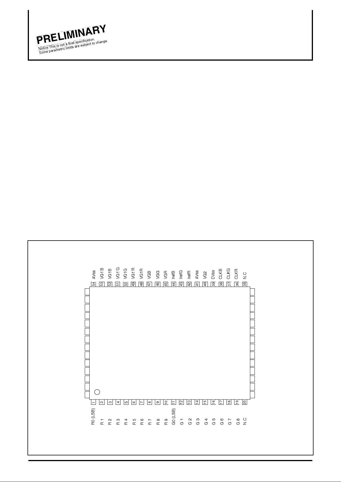
PIN CONFIGURATION (TOP VIEW)
VZ
IOUTR
IOUTRB
AVDD
AVDD
IOUTG
IOUTGB
AVDD
AVDD
IOUTB
IOUTBB
AVDD
AVDD
DVDD
55
56
57
58
59
60
61
62
63
64
65
66
67
68
M65530FP
34
33
32
31
30
29
28
27
26
25
24
23
22
21
N.C
CEB
BLK
B 9
B 8
B 7
B 6
B 5
B 4
B 3
B 2
B 1
B0(LSB)
G9
Outline 68P6S-A
NC:NO CONNECTION
1
Page 2
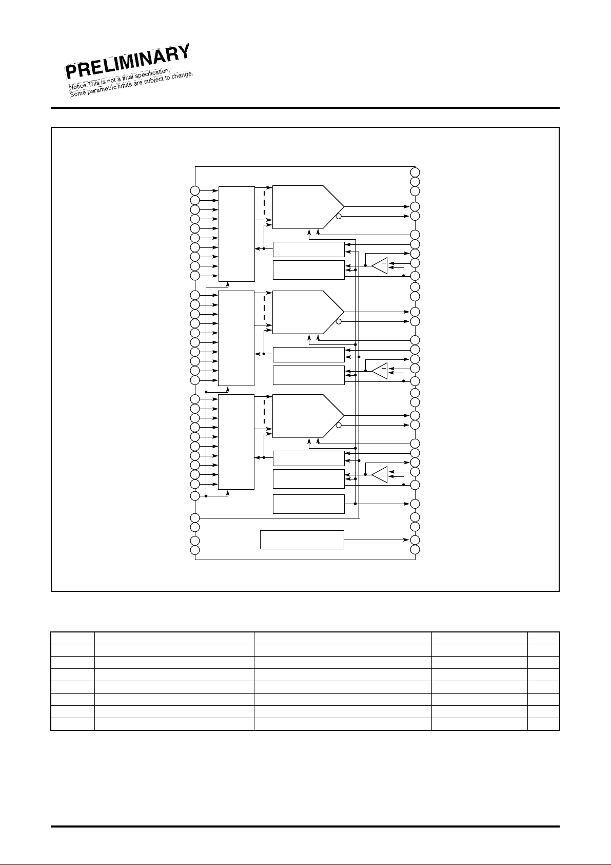
BLOCK DIAGRAM
R0(LSB)
R1
R2
R3
R4
R5
R6
R7
R8
R9
G0(LSB)
G1
G2
G3
G4
G5
G6
G7
G8
G9
B0(LSB)
B1
B2
B3
B4
B5
B6
B7
B8
B9
BLK
CEB
DVSS
N.C
N.C
MITSUBISHI ICs (AV COMMON)
M65530FP
TRIPLE 10-BIT VIDEO D-A CONVERTER
DVDD
68
AVDD
1
2
3
4
LATCH
5
&
6
DECODER
7
8
9
10
11
12
13
14
LATCH
15
&
16
DECODER
17
18
19
21
22
23
24
25
LATCH
26
&
27
DECODER
28
29
30
31
32
33
39
20
34
CURRENT
CELL
MATRIX
CLOCK DRIVER
REFERENCE
CURRENT SOURCE
CURRENT
CELL
MATRIX
CLOCK DRIVER
REFERENCE
CURRENT SOURCE
CURRENT
CELL
MATRIX
CLOCK DRIVER
REFERENCE
CURRENT SOURCE
REFERENCE
VOLTAGE SOURCE
VOLTAGE REGULATOR
67
66
AVDD
56
IOUTR
57
IOUTRB
49
VG1’R
36
CLKR
48
VG1R
45
42
63
62
60
61
51
37
50
46
43
59
58
64
65
53
38
52
47
44
40
54
41
55
35
VGR
IrefR
AVDD
AVDD
IOUTG
IOUTGB
VG1’G
CLKG
VG1G
VGG
IrefG
AVDD
AVDD
IOUTB
IOUTBB
VG1’B
CLKB
VG1B
VGB
IrefB
VG2
AVSS
AVSS
VZ
N.C
+
+
+
ABSOLUTE MAXIMUM RATINGS (Ta = 25°C, unless otherwise noted.)
Symbol Parameter Conditions Ratings Unit
DVDD Digital supply voltage Pin 68 0 to 7.0 V
AVDD Analog supply voltage Pin 58, 59, 62, 63, 66, 67 0 to 7.0 V
VID Digital input voltage Pin 1 to 19, 21 to 33, 36 to 38 0 to 7.0 V
IOUT Analog output current Pin 56, 57, 60, 61, 64, 65 -30 to 0 mA
Pd Power dissipation 900 mW
Topr Operating temperature 0 to +70 °C
Tstg Storage temperature -20 to +125 °C
In current measurement, (+) and (-) is corresponding to an inflow and an outflow current, respectively.
2
Page 3
MITSUBISHI ICs (AV COMMON)
M65530FP
TRIPLE 10-BIT VIDEO D-A CONVERTER
ELECTRICAL CHARACTERISTICS (Ta = 25°C, AVDD = DV DD = 5.00V, unless otherwise noted.)
Symbol Parameter Test conditions
Res Resolution 10 Bits
VDD Supply voltage 4.75 5.00 5.25 V
DIDD Digital supply current 8 mA
AIDD Analog supply current 100 mA
NL Integral nonlinearity RL=75Ω, Rref=750Ω ± 2.0 LSB
DNL Differential nonlinearity RL=75Ω, Rref=750Ω ± 0.5 LSB
VIH Digital input voltage "H" 2.15 VCC V
VIL Digital input voltage "L" 0 0.85 V
tsu Data set-up time 5 ns
th Data hold time 5 ns
ts Settling time RL=75Ω, Rref=750Ω, ±1%FS 25 ns
VFS Full-scale amplitude RL=75Ω, Rref=750Ω 2.0 VP-P
VZ Regulated voltage source 1.28 V
In current measurement, (+) and (-) is corresponding to an inflow and an outflow current, respectively.
Limits
Min. Typ. Max.
Unit
RECOMMENDED OPERATING CONDITIONS (Ta = 25°C, unless otherwise noted.)
Symbol Parameter
VDD Supply voltage 4.75 5.00 5.25 V
VIH Digital input voltage (High) 2.15 VCC V
VIL Digital input voltage (Low) 0 0.85 V
tWH Clock pulse width (High) 10 ns
tWL Clock pulse width (Low) 10 ns
tsu Set-up time 5 ns
th Hold time 5 ns
Limits
Min. Typ. Max.
Unit
3
Page 4

MITSUBISHI ICs (AV COMMON)
M65530FP
TRIPLE 10-BIT VIDEO D-A CONVERTER
DESCRIPTION OF PIN
Pin No. Name I/O Function It connects to ---
1 to 10 R0 to R9 I Digital input pin for a DAC (Red channel). DSP LSI
11 to 19, 21 G0 to G9 I Digital input pin for a DAC (Green channel). DSP LSI
20, 34, 35 N.C. -
22 to 31 B0 to B9 I Digital input pin for a DAC (Blue channel). DSP LSI
32 BLK I Analog output setting during a blanking interval. Control LSI
33 CEB I Power-down control during unused conditions. Control LSI
36 to 38 CLKR,G,B I Clock input. DSP LSI
39 DVSS - Digital ground. GND
40 VG2 O Reference voltage for a current switch. Bypass capacitor
41 AVSS - Analog ground. GND
42 to 44 IrefR,G,B O
45 to 47 VGR,G,B I
48, 50, 52 VG1R,G,B O Phase compensation for a reference current source.
49, 51, 53 VG1’R,G,B I
54 AVSS - Analog ground. GND
No connection.
It is grounded during actual use.
The resistor for a conversion between voltage and current is
connected to this pin.
A voltage input for an analog output current control.
It is connected to the VZ(pin 55) during an actual use.
A reference voltage input for a current matrix.
It is connected to VG1 according to the application.
GND
Current setting
resistor
Variable resistor
Phase compen.
capacitor
Phase compen.
capacitor
55 VZ O Reference voltage output. Bypass capacitor
56, 60, 64 I OUT R,G,B O Analog output.
57, 61, 65 I OUT RB,GB,BB O Inverse analog output. GND
58, 59, 62
63, 66, 67
68 DVDD - Digital supply voltage of 5.0V. Power supply
AVDD - Analog supply voltage of 5.0V. Power supply
Output terminal
(filter)
4
Page 5

MITSUBISHI ICs (AV COMMON)
TRIPLE 10-BIT VIDEO D-A CONVERTER
Table of an analog power-down function (pin 33)
Analog power-down signal Power-down function
"H" Power-down
"L" Normal operation
Table of a blanking function (pin 32)
Blanking signal Blanking function
"H" Blanking
"L" Normal operation
• A blanking operation sets an analog output to 0V on the first rising edge of the clock after a
blanking signal has become "H" regardless of a digital input code.
Table of an analog output function (iout)
Digital input code
9
MSB
1 1 1 1 1 1 1 1 1 1 2.0000V
1 1 1 1 1 1 1 1 1 0 1.9980V
8 7 6 5 4 3 2 1
0
LSB
Analog output voltage
M65530FP
1 0 0 0 0 0 0 0 0 0 1.0000V
0 1 1 1 1 1 1 1 1 1 0.9980V
0 0 0 0 0 0 0 0 0 1 0.0020V
0 0 0 0 0 0 0 0 0 0 0.0000V
Note : The analog output voltage is a theoretical value in the condition of VDD = 5.0V, VZ = 1.28V, Rref = 768Ω and RL = 75Ω.
INPUT / OUTPUT TIMING DIAGRAM
tsu
DATA INPUT
CLOCK INPUT
tWL
ANALOG OUTPUT
tds
50%
th
tWH
ts
+1%FS
-1%FS
10%
tpd
Where both BLK and CEB are low.
5
tds 7nS
tpd 10nS
Page 6

CURRENT SETTING RESISTOR (Rref) AND
OUTPUT LOAD RESISTOR (RL) (external components)
Full-scale output amplitude (VFS) of each D/A converter is ;
VFS = (VG / Rref) x 16 x RL (VP-P).
where VG = 1.28 V, Rref = 768 Ω, RL = 75 Ω and VDD = 5.0V.
The full-scale output of about 2.0 VP-P is available by setting RL and
Rref to 75 Ω and 768 Ω, respectively.
An output impedance of the analog output terminal is almost the
same as the load resistor (RL).
NOTES TO THE OPERATION
MITSUBISHI ICs (AV COMMON)
M65530FP
TRIPLE 10-BIT VIDEO D-A CONVERTER
1. Both a ground and a supply planes in a PCB should be as wide
as possible for reducing a parasitic inductance and resistance.
Especially, for the better performance, the analog plane needs to
be much wider.
2. A tantalum or electrolytic capacitor of 10µF or more and a
ceramic capacitor of 0.01µF are tied together, which are
connected between a digital supply and ground, also between a
analog supply and ground.
These capacitors should be placed as close as possible to the
IC.
They work as bypass capacitors for preventing a degradation in
the performance by a supply voltage
fluctuation caused by digital signals including a clock and digital
inputs and so on.
3. The analog output should be isolated as much as possible from a
clock and digital inputs, thus minimizing decoupling and
interactive noise.
6
Page 7

APPLICATION EXAMPLE
MITSUBISHI ICs (AV COMMON)
M65530FP
TRIPLE 10-BIT VIDEO D-A CONVERTER
68 58 57 56 5567 66 65 64 63 62 61 60 59
R0
R1
R2
R3
R4
R5
R6
R7
R8
R9
G0
G1
G2
G3
G4
G5
G6
G7
G8
1
2
3
4
5
6
7
8
9
10
11
12
13
14
15
16
17
18
19
20
R0(LSB)
R1
R2
R3
R4
R5
R6
R7
R8
R9
G0(LSB)
G1
G2
G3
G4
G5
G6
G7
G8
N.C
M65530FP
21 31 32 33 3422 23 24 25 26 27 28 29 30
AVSS
VG1’B
VG1B
VG1’G
VG1G
VG1’R
VG1R
VGB
VGG
VGR
lrefB
lrefG
lrefR
AVSS
VG2
DVSS
CLKB
CLKG
CLKR
N.C
54
53
52
51
50
49
48
47
46
45
44
43
42
41
40
39
38
37
36
35
0.01µ
0.01µ
0.01µ
0.01µ
750Ω
750Ω
750Ω
0.01µ
CLKB
CLKG
CLKR
Units Resistance : Ω
Capacitance : F
Digital power supply
Digital GND
Analog power supply
Analog GND
7
 Loading...