

Page 1
PRELIMINARY
)
j
Notice:This is not a final specification.
Some parametric limits are subject to change.
MITSUBISHI ICs (LSI)
M64403FP
ERROR CORRECTION WITH VARIABLE LENGTH AND DISTANCE
DESCRIPTION
The M64403FP performs the decoding for RS (Reed Solomon)
code which primitive polynomial:P (X)=X8+X4+X3+X2+1 and its
generation polynomial:G (X)=Π (X-αj).
M64403FP can set the code length and check byte length, so it is
d-2
=0
able to be adopted to various systems.
FEATURES
It adopts three stages pipe line operation (Syndrome stage,
Euclidean stage, Chen search & error value stage), so it realizes
high speed error correction operation.
Capable of erasure correcting function and it improves error
correction performance.
• Where error counts (e), erasure counts (ε) and design distance
(d) have followed restriction.
2e + ε < d
Capable of parameter register programing.
(1) Four kinds of code parameter which code length and check
byte length are programmable.
(Good for the product code that has plural code parameters.)
• Where, maximum code length (L) are 255 bytes and
maximum check byte length (d-1) are 16 bytes.
(2) Programmable for erasure threshold.
(3) Programmable for four kinds of decoding mode.
APPLICATION
DVD player, DVD-ROM (DVD:Digital Video Disc), DBS (Direct
Broadcasting by Satellite), High density floppy disk, Hard disk,
CATV (Cable TV), MD (Mini Disc), DVC (Digital Video Cassette),
DAT (Digital Audio Cassette), DCC (DIgital Compact Cassette),
DVB (Digital Video Broadcast), CD-DA (Compact Disc-Digital
Audio), CD-ROM (Compact Disc-Read Only Memory), other
communication systems and storage media etc.
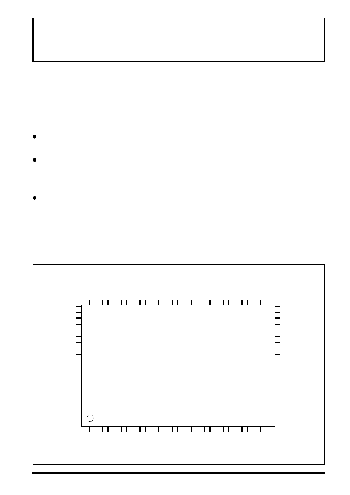
PIN CONFIGURATION(TOP VIEW
DAO7
DAO6
DIEN
LOEN
DAO5
MOD2
ELO1
ELO2
ELO3
ELO4
ELO5
ELO6
ELO7
SSO
V
DAM0
DAM1
DAM2
DAM3
DAM4
DAM5
DAM6
DAM7
V
DDO
OTRG
EREN
ADDC
VDDO
VSSI
ELO0
8079787776757473727170696867666564636261605958575655545352
81
82
83
84
85
86
87
88
89
90
91
92
93
94
95
96
97
98
99
100
2345678
1
DDO
VSSO
V
NOEN
DAO4
DAO3
MOD0
MOD1
SSO
DAO2
DAO1
DAO0
ENM4
ENM3
V
ENM2
M64403FP
9
101112131415161718
REST
READ
WRTE
CSEL
DHEF
PWDN
CLKO
Outline 100P6S-C
ENM1
ENM0
RES
DOEN
DDO
OUTR
UNCF
SYCR
V
2021222324252627282930
19
CLKE
ERMF
TESTE
SBFB
CLKI
TESM
ORDY
IRDY
SSO
V
DAI7
EROV
DAI6
TES3
DAI5
TES1
DAI4
SSO
V
SSI
V
VDDI
VDDI
CRDY
51
50
49
48
47
46
45
44
43
42
41
40
39
38
37
36
35
34
33
32
31
DAI3
CRDF
CORF
TES2
ERAF
TES7
V
DDO
OMD0
OMD1
OMD2
CLKM
SSO
V
RES
VDDO
ARM0
ARM1
ARM2
ARM3
DAI0
DAI1
DAI2
Page 2
PRELIMINARY
Notice:This is not a final specification.
Some parametric limits are subject to change.
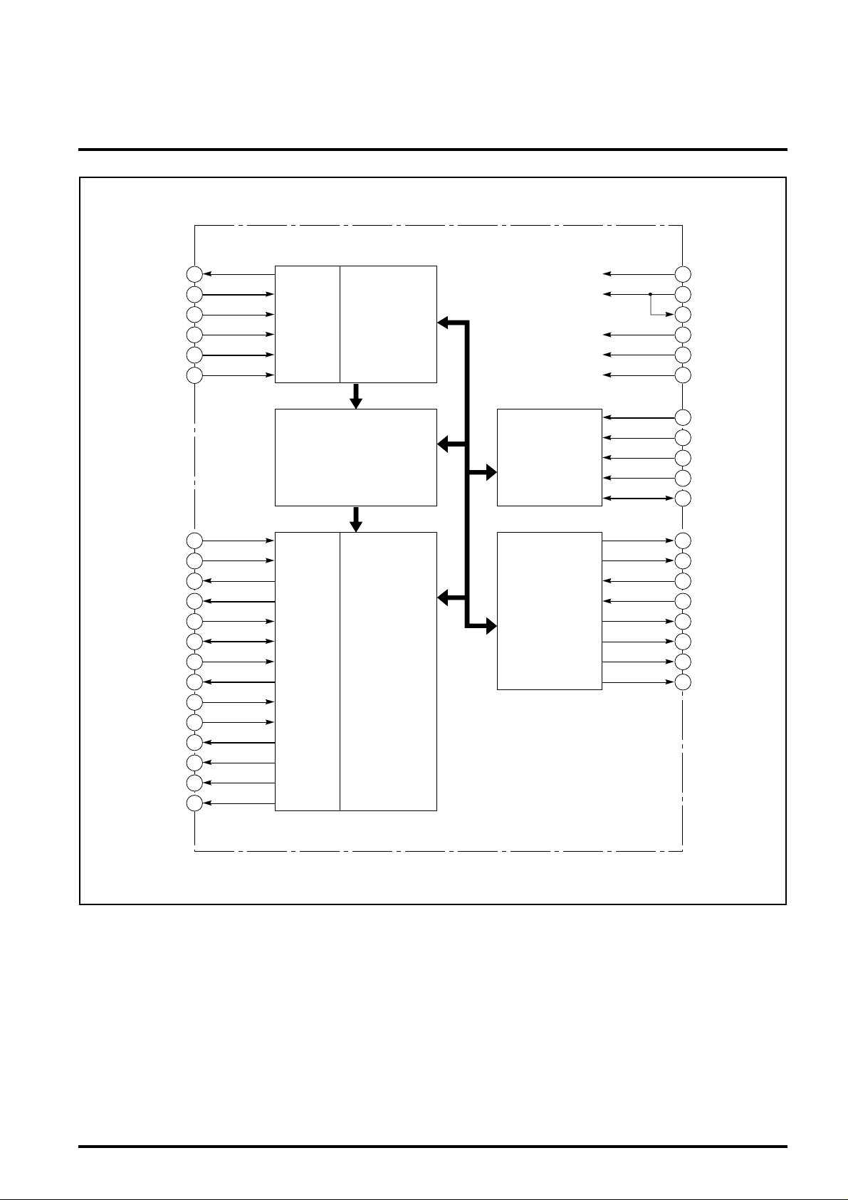
BLOCK DIAGRAM
MITSUBISHI ICs (LSI)
M64403FP
ERROR CORRECTION WITH VARIABLE LENGTH AND DISTANCE
IRDY
MOD0 – 2
DIEN
DHEF
DAI0 – 7
EREN
OTRG
ADDC
OUTR
DAO0 – 7
DOEN
ELO0 – 7
LOEN
ENM0 – 4
NOEN
ERMF
OMD0 – 2
CRDY
ORDY
CRDF
INPUT I/F
OUTPUT I/F
SYNDROME
CIRCUIT
EUCLIDEAN
CIRCUIT
CHEN SEARCH
ERROR VALUE
CIRCUIT
REST
CLKI
CLKM
CLKE
CLKO
PWDN
ARM0 – 3
MICRO
COMPUTER
I/F
CONTROL
CIRCUIT
&
CSEL
WRTE
READ
DAM0 – 7
SYCR
ERAF
TESTE
TESM
UNCF
CORF
EROV
SBFB
Page 3
PRELIMINARY
Notice:This is not a final specification.
Some parametric limits are subject to change.
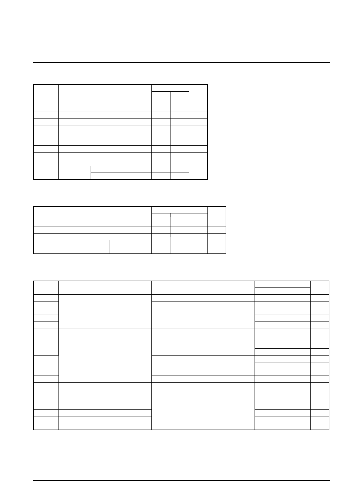
ABSOLUTE MAXIMUM RATINGS
Symbol UnitParameter
VDD VSupply voltage
VI Input voltage
VO
IIK Input protection diode current
OK
I
IO Output current
IDD VDD supply current
I
SS
Tstg Storage temperature
PdOUT
Output voltage
Output parasitic diode current
VSS supply current
Output
load
Output buffer@I
Output buffer@IOL=1mA
MITSUBISHI ICs (LSI)
M64403FP
ERROR CORRECTION WITH VARIABLE LENGTH AND DISTANCE
Ratings
MaxMin.
+6.5
-0.3
VDD+0.3
OL=4mA
-0.3
-0.3
DD+0.3
V
±20
±20
IOL=20
I
OH=-26
150-55
2200
760
81
81
V
V
mA
mA
mA
mA
mA
˚C
MHz•pF
RECOMMENDED OPERATING CONDITION
Symbol
VDD Supply voltage
Ta
VI
tr, tf
Operating temperature
Input voltage
Input rise & fall time
Parameter
Normal input
Schmit input
ELECTRICAL CHARACTERISTICS
Symbol
VIL
VIH
VTVT+
VH
VOL
VOH
Input voltage
(TTL interface)
Schmitt input voltage
(TTL interface)
Output voltage
IOL
Output current
IOH
IIL
IIH
IOZL
IOZH
RD
CI
CO
CIO
IDD
(∗ 1) : Rating for 4mA output buffer
(∗ 2) : Rating for 1mA output buffer
Input current
Output leak current
Pull down resistance
Input terminal capacitance
Output terminal capacitance
I/O terminal capacitance
Supply current
Parameter
Limits
Min. Typ. Max.
4.75 5.25
-20
5.0
+25
0
Test conditions
VDD=5.0V V
VDD=5.0V
+70
V
500
DD
Unit
V
˚C
V
nsec
5
msec
Limits
Min. Typ. Max.
0
2.2
5.25
Unit
0.8
1.350.7
DD=5.0V
V
2.21.4
1.20.3
V
DD=5.0V,
DD=4.5V, VOL=0.4V
V
IO <1µA
VDD=4.5V, VOH=4.1V
VDD5=5.5V, VI=0V
V
DD5=5.5V, VI=5.5V
V
DD5=5.5V, VI=0V
V
DD5=5.5V, VI=5.5V
V
DD5=5.0V, VI=5.0V
4.95
(∗1)
4
(∗2)
1
-1 +1
-1 +1
-1 +1
-1 +1
316
0.05
-4
-1
(∗3)
(∗4)
mA
mA
mA
mA
715
f=1MHz, V
DD=0V
715
715
mA
DD5=5.0V, VI=5.0V
V
2
V
V
V
V
V
V
µA
µA
µA
µA
kΩ
pF
pF
pF
Page 4
PRELIMINARY
Notice:This is not a final specification.
Some parametric limits are subject to change.
MICRO COMPUTER INTERFACE
Parameter register setting method (write) is described as follows.
(See page7 about sequence chart : See below diagram about
micro computer I/F and register table.)
1. Perform power on reset.
2. Set various parameters (code length-1, check byte length,
erasure correction threshold) to below parameter register table.
3. Set decode operation mode parameters to address-E. (See
address-E description)
See sequence chart page7 (micro computer I/F sequence) as for
read from parameter register, see below table as for register table.
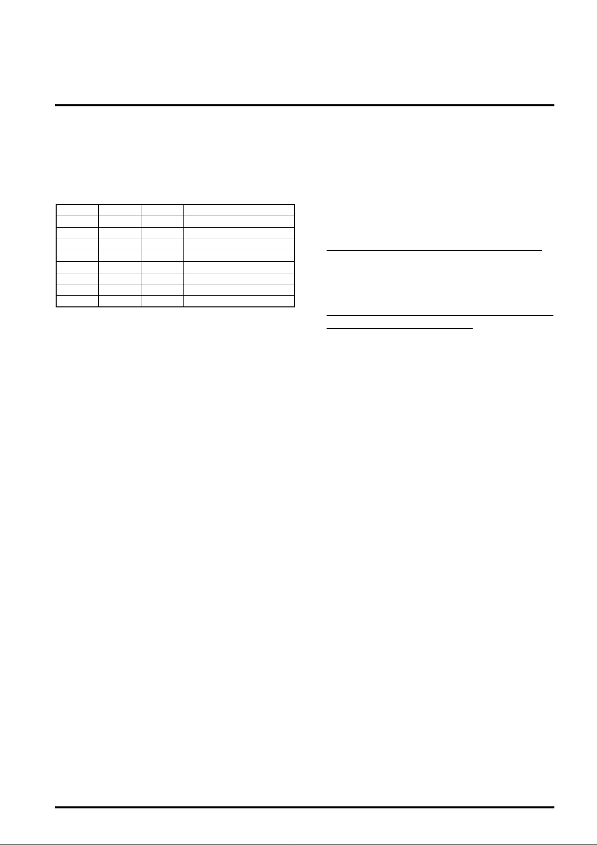
Parameter register table
address (Hex) R/W Initial (Hex) set data (Hex) description
00R/W1
00R/W2
00R/W3
00R/W4
00R/W5
00R/W6
00R/W7
00R/W8
00R/W9
00R/WA
00R/WB
—RC
——D
—R/WE
——F
ERROR CORRECTION WITH VARIABLE LENGTH AND DISTANCE
code (0) code length-1≤FE00R/W0
≤FE
≤FE
≤FE
≤10
≤10
≤10
≤10
≤10
≤10
≤10
≤10
—
—
—
—
code (1) code length-1
code (2) code length-1
code (3) code length-1
code (0) check byte length
code (1) check byte length
code (2) check byte length
code (3) check byte length
code (0) erasure threshold
code (1) erasure threshold
code (2) erasure threshold
code (3) erasure threshold
real erasure counts which is derived from syndrome calculation
reserve
decode operation mode
reserve
MITSUBISHI ICs (LSI)
M64403FP
Address-E description
address (Hex) data
ED7
D0 (bit0) 0:constrained error correction mode 1:erasure correction priority mode
D3 (bit3) 0:error value output mode 1:internal correction mode
D6 D5 D4 D3 D2 D1 D0
means "0" fixed.
Page 5
PRELIMINARY
Notice:This is not a final specification.
Some parametric limits are subject to change.
MITSUBISHI ICs (LSI)
M64403FP
ERROR CORRECTION WITH VARIABLE LENGTH AND DISTANCE
DECODE MODE SETTING METHOD
Decode mode is able to set at IRDY=H. Decode mode table is as
follows. Decode mode should be changed after all operations that
are set before changing.
Decodemode table
MOD0 MOD1 MOD2 mode
000
100
010
110
001
101
011
111
code (0) error correction
code (1) error correction
code (2) error correction
code (3) error correction
code (0) erasure correction
code (1) erasure correction
code (2) erasure correction
code (3) erasure correction
CODE WORD INPUT METHOD
Code word is able to input at IRDY=H. IRDY changes H to L when
head symbol for code word is input. And IRDY changes L to H
when the last symbol of code word is input.
DHEF should be H and DIEN should be L when the head symbol
of code word is input. DIEN is input enable signal for code word
and while it's L, input data is recognized as valid data and latched
to the internal circuit at rising edge of CLKI.
If the syndrome calculation for the 2nd code word finishes while the
1st code word is executed at Euclidean calculation stage, the
syndrome data that is latched internally is overwritten (called
syndrome collision) and the correcting operation for the 1st code
word is impossible. In this case, SYCR changes to H and informs
external of its status. (If the last symbol of code word is input at
SBFB=H, decoding is operated safely.)
SYCR which changes to H is reset by system reset (REST=L).
ERASURE FLAG INPUT METHOD AND
ERASURE CORRECTION MODE
Erasure correcting mode is set by the setting of erasure threshold
to address 8 to B for parameter register and the setting of
MOD2=H for decode mode signal. Erasure flag (EREN) should
input H by synchronization with symbol data of code word.
Follows are about erasure threshold.
(1) Constrained error correction mode is derived when the bit0 (D0)
of the parameter register address-E is set to L.
If the input erasure count is over the erasure threshold value ,
the operation is adopted ordinary error correction mode by
force.
(2) Erasure correction priority mode is derived when the bit0 (D0)
of the parameter register address-E is set to H.
If the error is detected at syndrome calculation and erasure
count is over the erasure threshold value , M64403FP regards
its operation as uncorrectable and correcting operation doesn't
execute.
In any cases ( , ), EROV (erasure over flag) changes to H.
(∗3) (∗4)
(∗4)
(∗3)
Page 6

PRELIMINARY
j
Notice:This is not a final specification.
Some parametric limits are subject to change.
MITSUBISHI ICs (LSI)
M64403FP
ERROR CORRECTION WITH VARIABLE LENGTH AND DISTANCE
CORRECTED DATA OUTPUT METHOD
When the decode operation finishes and correction result is able to
output to a code word, OUTR changes to H for one period for
CLKO. In this case, error location data is shown on ELO0 to ELO7,
error value is shown on DAO0 to DAO7 and error correction count
or erasure count is shown on ENM0 to ENM7. (Details are
described later.)
When output enable signals (LOEN, DOEN, NOEN) are set to L
(active mode), respective data (error location, error value, error or
erasure count) are able to output. When these output enable
signals are set to H, respective data bus change to high
impedance status.
Error location data (ELO0 to ELO7) 00 hex means the location of
head data for input code word.
Error value data (DAO0 to DAO7) corresponds with error location
data (ELO0 to ELO7).
ADDC should be L for one period of CLKO in order to output next
error location and next error value.
(See page10 : Correction data operation sequence chart)
ENM0 to ENM4 outputs error correcting count at ERMF=L, erasure
count at ERMF=H. This erasure count means real error count at
constrained error correction mode, total count for real error and
erasure at erasure correction priority mode. And this erasure count
includes empty erasure (it means error value is zero). If erasure
count excesses 31 dec, ENM0 to ENM4 shows 31 dec.
After the external circuit read error count/error location/error value
for a code word, OTRG should change L to H only one time by
synchronization with CLKO clock. Data shift for internal pipe line
circuit is executed by this operation. If this operation is so late,
registers in the internal pipe line become full. And data collision
may occur if code word is input more and its syndrome data is
generated. In this case, M64403FP informs external of its status
and SYCR changes to H. (If the last symbol of code word is input
at SBFB=H, decoding is operated safely.)
SYCR which changes to H is reset by system reset (REST=L).
OUTPUT CONTROL SIGNAL
When OUTR changes to H, CORF (error detected flag), UNCF
(uncorrectable flag) and EROV (erasure over flag) are output.
CORF changes to L when M64403FP regards input code word as
no error. CORF changes to H when M64403FP detects error.
UNCF changes to H when M64403FP regards the error correction
as impossible. If the input erasure flag count excesses erasure
threshold value with erasure correction priority mode, UNCF
changes to H also.
OMD0 to OMD2 show the current operated code word's decode
mode which was set by MOD0 to MOD2.
INTERNALCORRECTION MODE
The internal correction mode is active when the bit3 (D3) of
parameter register address-E is set to H. In this internal correction
mode, the code word that was input already and shown by OMD0
to OMD2 input to ELO0 to ELO7.
In order to recognize the header symbol of input data, OTRG
should be H by synchronization with the header symbol of code
word. ADDC should be L while valid code word is input.
Corrected data is output from DAO0 to DAO7 after three clocks
delay. OUTR changes to H by synchronization with header symbol
in order to show the header symbol of corrected code word. CRDY
changes to L by synchronization with output code word. CRDF
changes to H for corrected portion. In addition, ORDY changes to
H while output period of information symbol in order to distinguish
from code word from information symbol and check symbol.
MISOPERATION FOR ODD CHECK BYTE
NUMBER
M64403FP have no good operation when check byte number are
ust d/2 (d=check byte number+1) as UNCF don't to change to H,
and misdata is output.
But we can judge the misoperation when ENM<4:0> indicates d/2
in error correction mode, and ENM<4:0> indicates d/2 when
erasure number=0 or EROV=H in erasure correction mode.
Page 7

PRELIMINARY
Notice:This is not a final specification.
Some parametric limits are subject to change.
ERROR CORRECTION TIME
M64403FP is able to perform consecutive error correction
operation by bellowed three stage pipeline architecture.
• 1st stage...............Syndrome calculation
(operation step:A1=code length+20)
• 2nd stage............. Euclidean calculation
(operation step:A2=See table.2)
• 3rd stage..............Chen search & error value calculation
(operation step:A1=code length+20)
Table.1
pipe1
1st code
2nd code
3rd code
4th code
1st stage
2nd stage
1st stage 2nd stage
ERROR CORRECTION WITH VARIABLE LENGTH AND DISTANCE
pipe2
pipe3
3rd stage
1st stage
pipe4
correction
3rd stage
2nd stage
1st stage
pipe5
correction
3rd stage
2nd stage
MITSUBISHI ICs (LSI)
M64403FP
pipe6
correction
3rd stage
pipe7
correction
Table. 1 shows the operation flow in pipe line. As for the 1st code,
M64403FP output error correction data at pipe4 after 1st stage is
operated at pipe1, 2nd stage is operated at pipe2 and 3rd stage is
operated at pipe3. Therefore, the error correction has a latency of
three stages. The maximum step count for each pipe means the
maximum steps among above mentioned 1st stage to 3rd stage.
Where, the design distance decides the step count at the 2nd
stage. (See Table. 2)
Table.2
Design distance
Euclidean calculation steps
(erasure correction)
Euclidean calculation steps
(error correction)
17
330
290
16
290
270
15
260
250
14
230
220
210
190
(Ex.1)In the case of code length=100, design distance=11
A1=100+20=120, A2=160 A2>A1
So maximum operation step for one pipe is 160.
Therefore, correction data is obtained 480 steps (160 x
3) later from the input of 1st code word.
13
12
11
10
9
8
7
6
190
160
140
120
110
90
80
180
150
140
110
100
80
80
70
60
5
4
3
2
60
50
30
60
40
30
Page 8

PRELIMINARY
Notice:This is not a final specification.
Some parametric limits are subject to change.
CORRECTING OPERATION STEPS IN PIPE LINE
(Ex.1) code length=182, design distance=11
CLKI=CLKE=CLKO=25MHz error correction (no erasure)
202clk=8.08µs 202clk=8.08µs 202clk=8.08µs 202clk=8.08µs 202clk=8.08µs 202clk=8.08µs
ERROR CORRECTION WITH VARIABLE LENGTH AND DISTANCE
MITSUBISHI ICs (LSI)
M64403FP
1st code word
2nd code word
3rd code word
code word input
1st stage operation
Correction data is obtained three stages later (In this case, 202∗3=606clk 24.24µs) by input of consecutive code words.
2nd stage operation 3rd stage operation
code word input
1st stage operation
(Ex.2) code length=208, design distance=17
CLKI=CLKE=CLKO=25MHz erasure correction
290clk=11.6µs 290clk=11.6µs 290clk=11.6µs 290clk=11.6µs 290clk=11.6µs 290clk=11.6µs
correction data
access period
2nd stage operation 3rd stage operation
code word input
1st stage operation
2nd stage operation 3rd stage operation
correction data
access period
correction data
access period
1st code word
2nd code word
3rd code word
code word input
1st stage operation
Correction data is obtained three stages later (In this case, 290∗3=870clk 34.8µs) by input of consecutive code words.
2nd stage operation 3rd stage operation
code word input
1st stage operation
2nd stage operation 3rd stage operation
code word input
1st stage operation
correction data
access period
correction data
access period
2nd stage operation 3rd stage operation
correction data
access period
Page 9

PRELIMINARY
Notice:This is not a final specification.
Some parametric limits are subject to change.
MITSUBISHI ICs (LSI)
M64403FP
ERROR CORRECTION WITH VARIABLE LENGTH AND DISTANCE
address
data
address
address #2
data #2
data
data #1
address #1
MICRO COMPUTER I/F R/W SEQUENCE CHART
Note. READ=0 and WRTE=0 is inhibited at same time
ARM [3:0]
<WRITE>
CSEL
WRTE
1
READ
DMI [7:0]
ARM [3:0]
<READ1>
CSEL
1
WRTE
READ
DMO [7:0]
ARM [3:0]
<READ2>
CSEL
1
WRTE
READ
DMO [7:0]
Page 10

PRELIMINARY
Notice:This is not a final specification.
Some parametric limits are subject to change.
MITSUBISHI ICs (LSI)
M64403FP
ERROR CORRECTION WITH VARIABLE LENGTH AND DISTANCE
D4
03
XX
XX
D0 D1 D2 D3D181
(Renewal trigger to next step)
← Correcting data read finish
ERASURE COUNT=00
← Change to 1 after whole code word is input.
D4 D5
D3
D2
← Correction data renewal enable
Correction data output ready
P2
P0 P1
XX
L2
L0 L1
XX
03
0
CORRECTING DATA OPERATION SEQUENCE CHART
(Where necessary parameter is set already.)
CLKI
CLKO
REST
← Syndrome calculation is enable@IRDY=1:under calculation=0
IRDY
MOD [2:0]
DHEF=1, DIEN=0 are onlyheader symbol for code word.
DIEN
DHEF
D0 D1
DAI [7:0]
OTRG
ADDC
OUTR
ELO [7:0]
DAO [7:0]
ENM [4:0]
OMD [2:0]
ERMF
UNCF
1
CORF
EROV
Page 11

PRELIMINARY
Notice:This is not a final specification.
Some parametric limits are subject to change.
7 WORD06 WORD05 WORD04 WORD03 WORD02 WORD01 WORD0
MITSUBISHI ICs (LSI)
M64403FP
ERROR CORRECTION WITH VARIABLE LENGTH AND DISTANCE
54 3
4 5
uncorrectable status
3
2 3 4 5
2
1
2
1
no error status
correcting
status
1
CONSECUTIVE DECODE SEQUENCE CHART (1)
(Only one kind of code exists)
REST
IRDY
DAI [7:0]
DHEF
DAO [7:0]
ELO [7:0]
OUTR
OTRG
ADDC
UNCF
CORF
EROV
0
ERMF
Error value/location output zero at no error and uncorrectable state.
Note. DAO and LOE output first error value/location @ OUTR=H. After all of error value/location for error count are output, they output zero.
ENM [4:0]
Page 12

PRELIMINARY
Notice:This is not a final specification.
Some parametric limits are subject to change.
MITSUBISHI ICs (LSI)
M64403FP
ERROR CORRECTION WITH VARIABLE LENGTH AND DISTANCE
11
11
n code
12 WORD n 13 WORD n
11 WORD n
10
10
111098
decoding operation mode for n code
1
REST
CONSECTIVE DECODE SEQUENCE CHART (2)
(Ex : Two kinds of code parameter exist (Product code))
IRDY
10 WORD m
9 WORD m
DAI [7:0]
m code
decoding operation mode for m code decoding operation mode for n code
MOD [2:0]
98
DAO [7:0]
9
8
ELO [7:0]
OUTR
OTRG
ADDC
UNCF
CORF
EROV
0
ERMF
ENM [4:0]
decoding operation mode for m code
Error value/location output zero at no error and uncorrectable state.
Note. DAO and LOE output first error value/location @ OUTR=H. After all of error value/location for error count are output, they output zero.
OMD [2:0]
Page 13

PRELIMINARY
Notice:This is not a final specification.
Some parametric limits are subject to change.
EXAMPLE FLOW CHART FOR GENERAL
PRODUCT CODE DECODING
In the case of C1→C2→C1 repeat correction as a decoding method
ERROR CORRECTION WITH VARIABLE LENGTH AND DISTANCE
START
MITSUBISHI ICs (LSI)
M64403FP
PWDN=0
Yes
PWDN=1
REST=L→H
Set decoding mode parameter register
address-E.
(Example)
Set C1's error corection mode for
code (0) and C2's erasure correction
mode for code (1)
No
-Example for product code constitution-
Code word for C1 direction
Code word C2
direction
Set necessary data to the parameter
register address 0 to B
1
Page 14

PRELIMINARY
Notice:This is not a final specification.
Some parametric limits are subject to change.
1
Set decoding mode
Set MOD [0:2] for
C1 (1st time)
MITSUBISHI ICs (LSI)
M64403FP
ERROR CORRECTION WITH VARIABLE LENGTH AND DISTANCE
Set decoding mode
Set MOD [0:2] to
C2
Recognition of
header symbol
for code word
DHEF=1?
Yes
C1 (1) decode
C1 (1)
decode
finish?
Yes
No
No
Recognition of
header symbol
for code word
DHEF=1?
Yes
C2decode
C2
decode
finish?
Yes
Set decoding mode
Set MOD [0:2] to
C1 (2nd time)
Recognition of
header symbol
for code word
DHEF=1?
Yes
No
No
No
C1 (2) decode
C1 (2)
decode
finish?
Yes
1
No
Page 15

PRELIMINARY
Notice:This is not a final specification.
Some parametric limits are subject to change.
INPUT TIMING
MITSUBISHI ICs (LSI)
M64403FP
ERROR CORRECTION WITH VARIABLE LENGTH AND DISTANCE
tc (CLKI)
tw (CLKI)
CLKI
DAI<7:0>
EREN
DIEN
MOD<2:0>
DHEF
TESTE
CLKO
OTRG
ADDC
ELO<7:0>
tsu (CLKI) th (CLKI)
tw (CLKO)
tsu (CLKO) th (CLKO)
tcw
tc (CLKO)
Symbol
tc (CLKI) CLKI clock period
tw (CLKI)
tsu (CLKI)
CLKI clock pulse width
CLKI setup time
CLKI hold timeth (CLKI) 10
Symbol
tc (CLKO)
tw (CLKO)
tsu (CLKO)
th (CLKO)
CLKO clock period
CLKO clock pulse width
CLKO setup time
CLKO hold time
Parameter
Parameter
Limits
(Min.)
40
16
Limits
(Min.)
40
16
10
Unit
ns
ns
ns
5
ns
Unit
ns
ns
5
ns
ns
ARM<3:0>
CSEL
WRTE
DAM<7:0>
tsu (A) tsu (C) trec (W)
tw (W)
tsu (D) th (D)
Symbol
tcw
tsu (A)
tsu (C)
trec (W) 10
tw (W)
tsu (D)
th (D)
Write cycle time
Address setup time
Chip select setup time
Write recovery time
Write ulse width
Data setup time
data hold time
Parameter
Limits
(Min.)
40
10
10
10
10 ns
Unit
ns
ns
ns
ns
ns
5ns
Page 16

PRELIMINARY
Notice:This is not a final specification.
Some parametric limits are subject to change.
OUTPUT TIMING
At output load capacity=50pF
MITSUBISHI ICs (LSI)
M64403FP
ERROR CORRECTION WITH VARIABLE LENGTH AND DISTANCE
CLKO
ENM<4:0>
DAO<7:0>
ELO<7:0>
UNCF
CORF
OUTR
OMD<2:0>
CLKI
SYCR
NOEN
DOEN
LOEN
ENM<4:0>
DAO<7:0>
ELO<7:0>
td (CKO)
td (CKI)
Symbol
td (CKO)
Symbol
td (CKI)
Symbol
ta (OE)
tdis (OE)
Parameter
CLKO output propagation time
Parameter
CLKI output propagation time
Parameter
Output enable time
Output disable time
Limits
(Max.)
20
Limits
(Max.)
20
Limits
(Max.)
15
15
Unit
ns
Unit
ns
Unit
ns
ns
ARM<3:0>
CSEL
READ
DAM<7:0>
ta (OE) tdis (OE)
tcr
ta (A)
ta (C)
ta (R)
tdis (C)
tdis (R)
Symbol
tcr
ta (A)
ta (C)
ta (R)
tdis (C)
tdis (R)
Parameter
Read cycle time
Address access time
Chip select access time
Output enable access time
Output disable access time (from CSEL)
Output disable access time (from READ)
Limits
40 (min)
10 (max)
10 (max)
10 (max)
10 (max)
10 (max)
Unit
ns
ns
ns
ns
ns
ns
Page 17

PRELIMINARY
↓↓↓
↓
Notice:This is not a final specification.
Some parametric limits are subject to change.
DESCRIPTIO N OF PIN
Pin No.
1, 23, 40,
53, 70, 88
2, 38, 45,
61, 79, 97
16, 39
28, 80
29, 52
3
4
5
6 to 8
9
10
11
12
13
14
15
17
18
19
20
21
22
24 to 27
30 to 33
34 to 37
41
42 to 44
46
47
48
49
50
51
54
55
56
57
58
59
60
62
63
64 to 68
69, 71 to 77
78, 81 to 87
89 to 96
98
99
100
Name
VSSO
DDO
V
RES
VSSI
VDDI
NOEN
LOEN
DIEN
MOD2 to MOD0
WRTE
READ
CSEL
PWDN
REST
DHEF
CLKO
DOEN
CLKE
ERMF
TESTE
TESM
CLKI
DAI7 to DAI4
DAI3 to DAI0
ARM3 to ARM0
CLKM
OMD2 to OMD0
TES7
ERAF
TES2
CORF
CRDF
CRDY
TES1
TES3
EROV
IRDY
ORDY
OUTR
SBFB
SYCR
UNCF
ENM0 to ENM4
DAO0 to DAO7
ELO0 to ELO7
DAM0 to DAM7
OTRG
EREN
ADDC
I/O
—
—
—
—
—
I
I
I
I
I
I
I
I
I
I
I
I
I
I
I
I
I
I
I
O
O
O
O
O
O
O
O
O
O
O
O
O
O
O
O
O
O
O
I/O
I/O
I
I
I
I/O structure
TTL input
TTL input
TTL input
TTL input
TTL schmitt trigger input
TTL schmitt trigger input
TTL schmitt trigger input
TTL schmitt trigger input
TTL schmitt trigger input
TTL input
TTL schmitt trigger input
TTL input
TTL input
TTL input
TTL input
TTL input
TTL schmitt trigger input
TTL input
TTL input
TTL output (4mA)
TTL output (4mA)
TTL output (1mA)
TTL output (4mA)
TTL output (4mA)
TTL output (4mA)
TTL output (4mA)
TTL output (4mA)
TTL output (4mA)
TTL output (4mA)
TTL output (4mA)
TTL output (4mA)
TTL output (4mA)
TTL output (4mA)
TTL output (4mA)
TTL output (4mA)
TTL output (4mA)
TTL3 state output (4mA)
TTL3 state output (4mA)
TTL I/O
(Pull down Rd=2kΩ)
TTL I/O
(Pull down Rd=2kΩ)
TTL input
TTL output (4mA)
TTL input
MITSUBISHI ICs (LSI)
M64403FP
ERROR CORRECTION WITH VARIABLE LENGTH AND DISTANCE
I/O type
—
—
—
—
—
—
—
—
—
—
T22N
T22N
T22N
T22N
U22N
U22N
U22N
U22N
U22N
T22N
U22N
T22N
T22N
T22N
T22N
T22N
U22N
T22N
T22N
O65T
O65T
O63T
O65T
O65T
O65T
O65T
O65T
O65T
O65T
O65T
O65T
O65T
O65T
O65T
O65T
O65T
Z65T
Z65T
TH2N
TH2N
T22N
O65T
T22N
GND for output
+5V for output
reserve
GND for input
+5V for input
output enable for ENM0 to 4 0:Enable 1:HiZ
output enable for ELO0 to 7 0:Enable 1:HiZ
Symbol data input enable 0:Enable
decoding mode setting MOD2:MSB MOD0:LSB
micro computer I/F write enable 0:Enable
micro computer I/F read enable 0:Enable
micro computer I/F chip select 0:Select
power save 0:power save
system reset 0:Reset
symbol data header 1:Data head
data output clock (Typ.13.5MHz)
output enable for DAO0 to 7 0:Enable 1:HiZ
internal operation clock (Typ.13.5MHz)
output enable for ENM0 to 7 1:erasure counts 0:correcting counts
test mode selection 0:decoding 1:testing
test mode selection 0:decoding 1:testing
symbol data input clock (Typ.13.5MHz)
symbol data input bus DAI7:MSB
micro computer I/F address bus ARM3:MSB ARM0:LSB
CLKI monitor (Typ.13.5MHz)
decoded operation mode (relative to MOD0 to 2)
test monitor output
erasure flag output 1:Enable
test monitor output
error detection flag 0:No Error 1:detected
correction flag 1:corrected data
output valid flag 0:valid
test monitor output
test monitor output
erasure over flag 1:over
symbol data input ready 1:Ready
data flag 0:data
output ready 1:Ready/output data header
(@ internal correction mode) 1:header
syndrome data collision prevention signal
syndrome data collision alarm 1:alarm (collision)
uncorrectable flag 1:Uncorrect
error correction counts/erasure counts output bus ENM4:MSB ENM0:LSB
error value output bus DAO7:MSB DAO0:LSB
data input (for correction) /error location output bus
ELO7:MSB ELO0:LSB
micro computer I/F bus DAM7:MSB DAM0:LSB
renewal trigger 0→1:renewal/input data
(@internal correction mode) 1:header
erasure flag input 1:@erasure input
output data renewal 0:Next/code word valid
(@internal correction mode) 0:valid
Description of function
DAI0:LSB
 Loading...