

Page 1
PRELIMINARY
Notice: This is not a final specification.
Some parametric limits are subject to change.
MITSUBISHI SEMICONDUCTOR <TRANSISTOR ARRAY>
M63813P/FP/GP/KP
7-UNIT 300mA TRANSISTOR ARRAY WITH CLAMP DIODE
DESCRIPTION
M63813P/FP/GP/KP are seven-circuit Single transistor arrays with clamping diodes. The circuits are made of NPN
transistors. Both the semiconductor integrated circuits perform high-current driving with extremely low input-current
supply.
FEATURES
●
Four package configurations (P, FP, GP and KP)
●
Medium breakdown voltage (BVCEO ≥ 35V)
●
Synchronizing current (IC(max) = 300mA)
●
With clamping diodes
●
Low output saturation voltage
●
Wide operating temperature range (Ta = –40 to +85 °C)
APPLICATION
Driving of digit drives of indication elements (LEDs and
lamps) with small signals
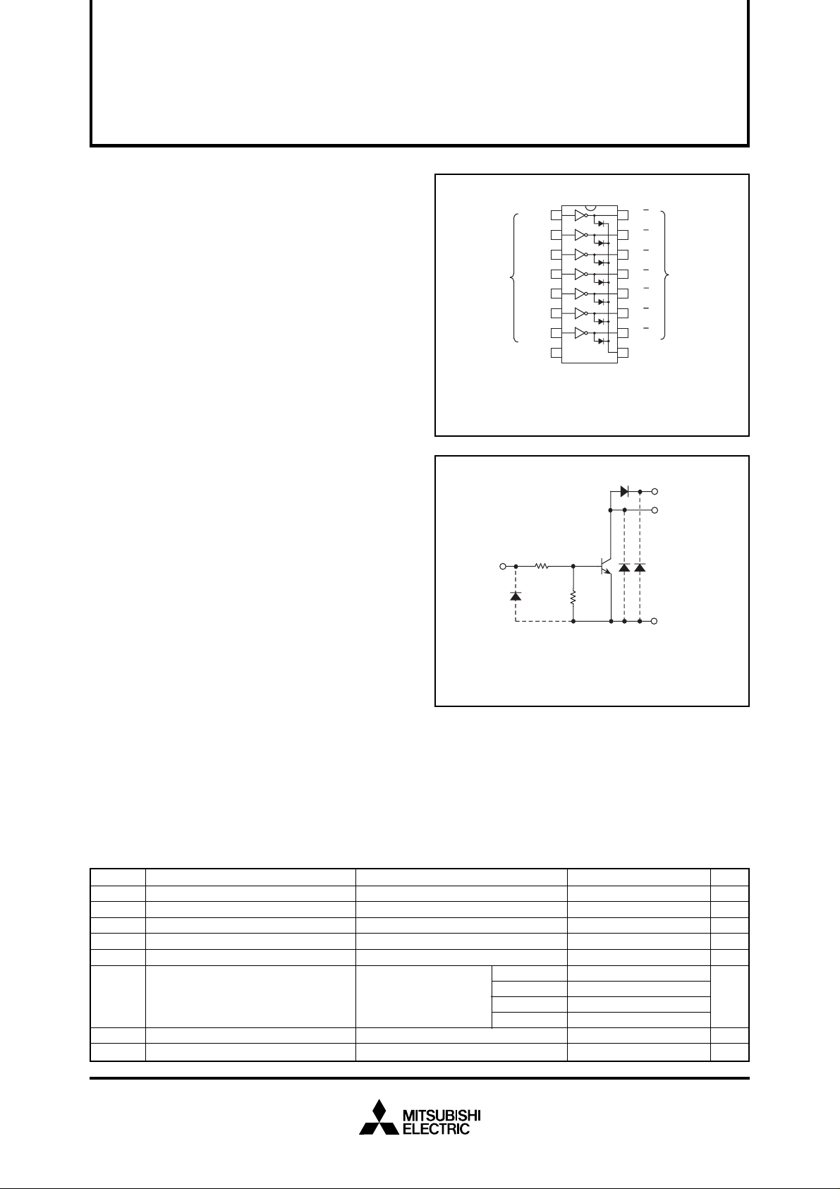
PIN CONFIGURATION
→
IN1
→
IN2
→
INz3
→
IN4
INPUT
→
IN5
→
IN6
→
IN7
GND
Package type
CIRCUIT DIAGRAM
INPUT
2.7k
→
16
1
2
3
4
5
611
7
8
O1
→
15
O2
→
14
O3
→
13
O4
12
→O5
→
O6
→
10
O7
9
→
COM COMMOM
OUTPUT
16P4(P)
16P2N-A(FP)
16P2S-A(GP)
16P2Z-A(KP)
COM
OUTPUT
10k
GND
FUNCTION
The M63813P/FP/GP/KP each have seven circuits consist-
The diode, indicated with the dotted line, is parasitic, and
cannot be used.
ing of NPN transistor. A spike-killer clamping diode is provided between each output pin (collector) and COM pin
(pin9). The transistor emitters are all connected to the GND
pin (pin 8). The transistors allow synchronous flow of 300mA
collector current. A maximum of 35V voltage can be applied
between the collector and emitter.
ABSOLUTE MAXIMUM RATINGS (Unless otherwise noted, Ta = –40 ~ +85°C)
VCEO
IC
VI
IF
VR
Pd
Topr
Tstg
Collector-emitter voltage
Collector current
Input voltage
Clamping diode forward current
Clamping diode reverse voltage
Power dissipation
Operating temperature
Storage temperature
Output, H
Current per circuit output, L
Ta = 25°C, when mounted
on board
The seven circuits share the COM and GND.
RatingsSymbol Parameter Conditions Unit
–0.5 ~ +35
300
–0.5 ~ +35
300
35
M63813P
M63813FP
M63813GP
M63813KP
1.47
1.00
0.80
0.78
–40 ~ +85
–55 ~ +125
Unit: Ω
V
mA
V
mA
V
W
°C
°C
Jan. 2000
Page 2
MITSUBISHI SEMICONDUCTOR <TRANSISTOR ARRAY>
M63813P/FP/GP/KP
PRELIMINARY
Notice: This is not a final specification.
Some parametric limits are subject to change.
RECOMMENDED OPERATING CONDITIONS (Unless otherwise noted, Ta = –40 ~ +85°C)
Symbol UnitParameter Test conditions
VO V0
IC
Output voltage
Collector current
(Current per 1 circuit when 7 circuits
are coming on simultaneously)
M63813P
M63813FP
M63813GP
M63813KP
Duty Cycle no more than 45%
Duty Cycle no more than 100%
Duty Cycle no more than 30%
Duty Cycle no more than 100%
Duty Cycle no more than 24%
Duty Cycle no more than 100%
Duty Cycle no more than 24%
Duty Cycle no more than 100%
VIN Input voltage
ELECTRICAL CHARACTERISTICS (Unless otherwise noted, Ta = 25°C)
Symbol UnitParameter Test conditions
V
(BR) CEO
CE(sat)
V
VIN(on)
VF
IR
hFE
Collector-emitter breakdown voltage
Collector-emitter saturation voltage
“On” input voltage
Clamping diode forward volltage
Clamping diode reverse current
DC amplification factor
I
CEO = 10µA
IN = 1mA, IC = 10mA
I
IN = 2mA, IC = 150mA
I
IN = 1mA, IC = 10mA
I
F = 250mA
I
R = 35V
V
CE = 10V, IC = 10mA
V
7-UNIT 300mA TRANSISTOR ARRAY WITH CLAMP DIODE
Limits
min typ max
—
0
0
0
0
0
0
0
0
0
—
—
—
—
—
—
—
—
—
35
250
160
250
130
250
120
250
120
20
Limits
min typ max
35
—
—
2.4
—
—
50
1.2
—
—
—
35
—
—
—
0.2
0.8
4.2
2.0
10
—
mA
V
V
V
V
V
µA
—
SWITCHING CHARACTERISTICS (Unless otherwise noted, Ta = 25°C)
Symbol UnitParameter Test conditions
ton
toff
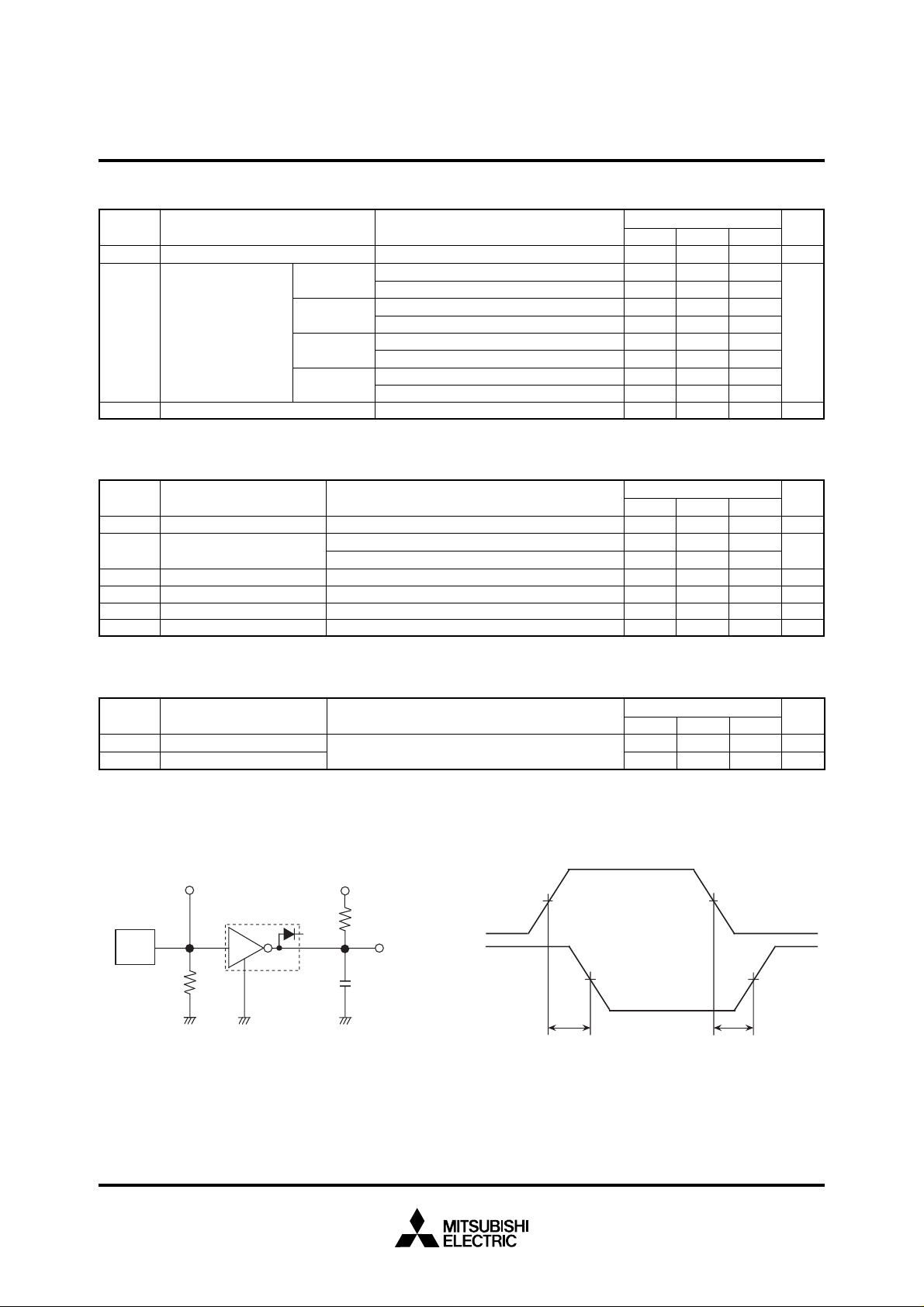
NOTE 1 TEST CIRCUIT
Turn-on time
Turn-off time
INPUT
Measured device
PG
50Ω
(1)Pulse generator (PG) characteristics : PRR = 1kHz,
tw = 10µs, tr = 6ns, tf = 6ns, Zo = 50Ω, V
(2)Input-output conditions : R
(3)Electrostatic capacity C
connections and input capacitance at probes
OPEN
L
= 220Ω, Vo = 35V
L
includes floating capacitance at
CL = 15pF (note 1)
Vo
R
L
OUTPUT
L
C
IH
= 3V
TIMING DIAGRAM
INPUT
OUTPUT
50%
ton toff
Limits
min typ max
—
—
125
250
—
—
50%
ns
ns
50%50%
Jan. 2000
Page 3

PRELIMINARY
Notice: This is not a final specification.
Some parametric limits are subject to change.
TYPICAL CHARACTERISTICS
MITSUBISHI SEMICONDUCTOR <TRANSISTOR ARRAY>
M63813P/FP/GP/KP
7-UNIT 300mA TRANSISTOR ARRAY WITH CLAMP DIODE
Thermal Derating Factor Characteristics
2.0
M63813P
1.5
M63813FP
1.0
M63813GP
M63813KP
0.5
Power dissipation Pd (W)
0
0 25 50 75 10085
Ambient temperature Ta (°C)
Duty Cycle-Collector Characteristics
(M63813P)
400
300
200
•The collector current values
100
Collector current Ic (mA)
represent the current per circuit.
•Repeated frequency ≥ 10Hz
•The value the circle represents the value of
the simultaneously-operated circuit.
•Ta = 25°C
0
20 40 60 80
0
0.744
0.520
0.418
0.406
100
1~4
5
6
7
Input Characteristics
8
Ta = –40°C
6
(mA)
I
4
Input current I
2
0
02015105
Input voltage V
Duty Cycle-Collector Characteristics
(M63813P)
400
300
200
•The collector current values
100
represent the current per circuit.
Collector current Ic (mA)
•Repeated frequency ≥ 10Hz
•The value the circle represents the value of
the simultaneously-operated circuit.
•Ta = 85°C
0
0
20 40 60 80
Ta = 25°C
Ta = 85°C
I
(V)
100
1~2
3
4
5
6
7
Duty cycle (%)
Duty Cycle-Collector Characteristics
400
(M63813FP)
300
200
•The collector current values
100
Collector current Ic (mA)
represent the current per circuit.
•Repeated frequency ≥ 10Hz
•The value the circle represents the value of
the simultaneously-operated circuit.
•Ta = 25°C
0
20 40 60 80
0
Duty cycle (%)
100
1~3
4
5
6
7
Duty cycle (%)
Duty Cycle-Collector Characteristics
400
(M63813FP)
300
200
•The collector current values
represent the current per circuit.
100
Collector current Ic (mA)
•Repeated frequency ≥ 10Hz
•The value the circle represents the value of
the simultaneously-operated circuit.
•Ta = 85°C
0
0
20 40 60 80
Duty cycle (%)
100
1
2
3
4
5
6
7
Jan. 2000
Page 4

PRELIMINARY
Notice: This is not a final specification.
Some parametric limits are subject to change.
MITSUBISHI SEMICONDUCTOR <TRANSISTOR ARRAY>
M63813P/FP/GP/KP
7-UNIT 300mA TRANSISTOR ARRAY WITH CLAMP DIODE
Duty Cycle-Collector Characteristics
400
(M63813GP/KP)
300
200
•The collector current values
100
Collector current Ic (mA)
represent the current per circuit.
•Repeated frequency ≥ 10Hz
•The value the circle represents the value of
the simultaneously-operated circuit.
•Ta = 25°C
0
0
20 40 60 80
Duty cycle (%)
Output Saturation Voltage
Collector Current Characteristics
250
Ta = 25°C
IB = 3mA
200
150
100
Collector current Ic (mA)
50
IB = 2mA
I
B
= 0.5mA
I
B
= 1.5mA
I
B
= 1mA
100
1~2
3
4
5
6
7
Duty Cycle-Collector Characteristics
400
(M63813GP/KP)
300
200
•The collector current values
100
Collector current Ic (mA)
represent the current per circuit.
•Repeated frequency ≥ 10Hz
•The value the circle represents the value of
the simultaneously-operated circuit.
•Ta = 85°C
0
0
20 40 60 80
Duty cycle (%)
Output Saturation Voltage
Collector Current Characteristics
100
Ta = 25°C
80
V
I
V
I
= 6V
= 7V
60
40
20
Collector current Ic (mA)
V
V
I
= 2V
I
= 3V
VI = 5V
V
I
= 4V
100
1
2
3
4
5
6
7
0
0 0.2 0.4 0.6 0.8
Output saturation voltage V
Output Saturation Voltage
Collector Current Characteristics
100
II = 2mA
80
Ta = –40°C
60
40
20
Collector current Ic (mA)
0
0 0.05 0.10 0.15 0.20
Output saturation voltage V
CE(sat)
Ta = 25°C
Ta = 85°C
CE(sat)
(V)
(V)
0
0 0.05 0.10 0.15 0.20
Output saturation voltage V
DC Amplification Factor
Collector Current Characteristics
3
10
VCE 10V
7
Ta = 25°C
5
FE
3
2
2
10
7
5
3
DC amplification factor h
2
1
10
0
2357 2357
10
10
1
10
Collector current Ic (mA)
CE(sat)
2
23 57
(V)
10
3
Jan. 2000
Page 5

PRELIMINARY
Notice: This is not a final specification.
Some parametric limits are subject to change.
MITSUBISHI SEMICONDUCTOR <TRANSISTOR ARRAY>
M63813P/FP/GP/KP
7-UNIT 300mA TRANSISTOR ARRAY WITH CLAMP DIODE
Grounded Emitter Transfer Characteristics
50
VCE = 4V
40
Ta = 25°C
Ta = 85°C
0 0.4 0.8 1.2 1.6 2.0
Input voltage V
I
Collector current Ic (mA)
30
20
10
0
Clamping Diode Characteristics
250
200
(mA)
F
150
Ta = 85°C
Ta = –40°C
(V)
Grounded Emitter Transfer Characteristics
250
VCE = 4V
200
Ta = 85°C
150
Ta = 25°C
100
Collector current Ic (mA)
50
0
012345
Input voltage V
Ta = –40°C
I
(V)
100
Ta = 25°C
50
Forward bisa current I
0
0 0.4 0.8 1.2 1.6 2.0
Forward bias voltage V
Ta = –40°C
F
(V)
Jan. 2000
 Loading...