

Page 1
PRELIMINARY
Notice: This is not a final specification.
Some parametric limits are subject to change.
MITSUBISHI SEMICONDUCTOR <TRANSISTOR ARRAY>
M63807P/FP/KP
8-UNIT 300mA TRANSISTOR ARRAY
DESCRIPTION
M63807P/FP/KP are eight-circuit Single transistor arrays.
The circuits are made of NPN transistors. Both the semiconductor integrated circuits perform high-current driving with
extremely low input-current supply.
FEATURES
●
Three package configurations (P, FP, and KP)
●
Medium breakdown voltage (BVCEO ≥ 35V)
●
Synchronizing current (IC(max) = 300mA)
●
Low output saturation voltage
●
Wide operating temperature range (Ta = –40 to +85°C)
APPLICATION
Driving of digit drives of indication elements (LEDs and
lamps) with small signals
FUNCTION
The M63807P/FP/KP each have eight circuits consisting of
NPN transistor. The transistor emitters are all connected to
the GND pin. The transistors allow synchronous flow of
300mA collector current. A maximum of 35V voltage can be
applied between the collector and emitter.
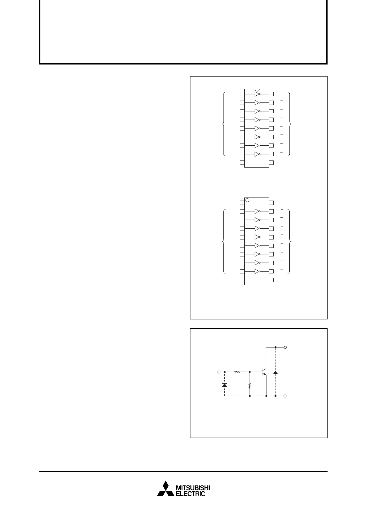
PIN CONFIGURATION
1
IN1→
→
IN2
2
→
3
IN3
→
4
IN4
INPUT
→
5
IN5
→
613
IN6
→
IN7
7
8
→
IN8
GND
9
Package type
1
→
2
IN1
→
IN2
3
→
4
IN3
→
5
IN4
INPUT OUTPUT
IN5
IN6
IN7
IN8
GND
→
6
→
7
→
8
→
9
10
18
17
16
15
14
12
11
10
18P4G(P)
20
19
18
17
16
15
14
13
12
11
20P2N-A(FP)
Package type
20P2E-A(KP)
→
O1
→
O2
→
O3
→
O4
OUTPUT
→
O5
→
O6
→
O7
→
O8
→
NC
NCNC
→
O1
→
O2
→
O3
→
O4
→
O5
→
O6
→
O7
→
O8
→
NC
NC : No connection
CIRCUIT DIAGRAM
INPUT
The diode, indicated with the dotted line, is parasitic, and
cannot be used.
10.5K
10K
The eight circuits share the GND.
OUTPUT
GND
Unit: Ω
Jan. 2000
Page 2
MITSUBISHI SEMICONDUCTOR <TRANSISTOR ARRAY>
PRELIMINARY
Notice: This is not a final specification.
Some parametric limits are subject to change.
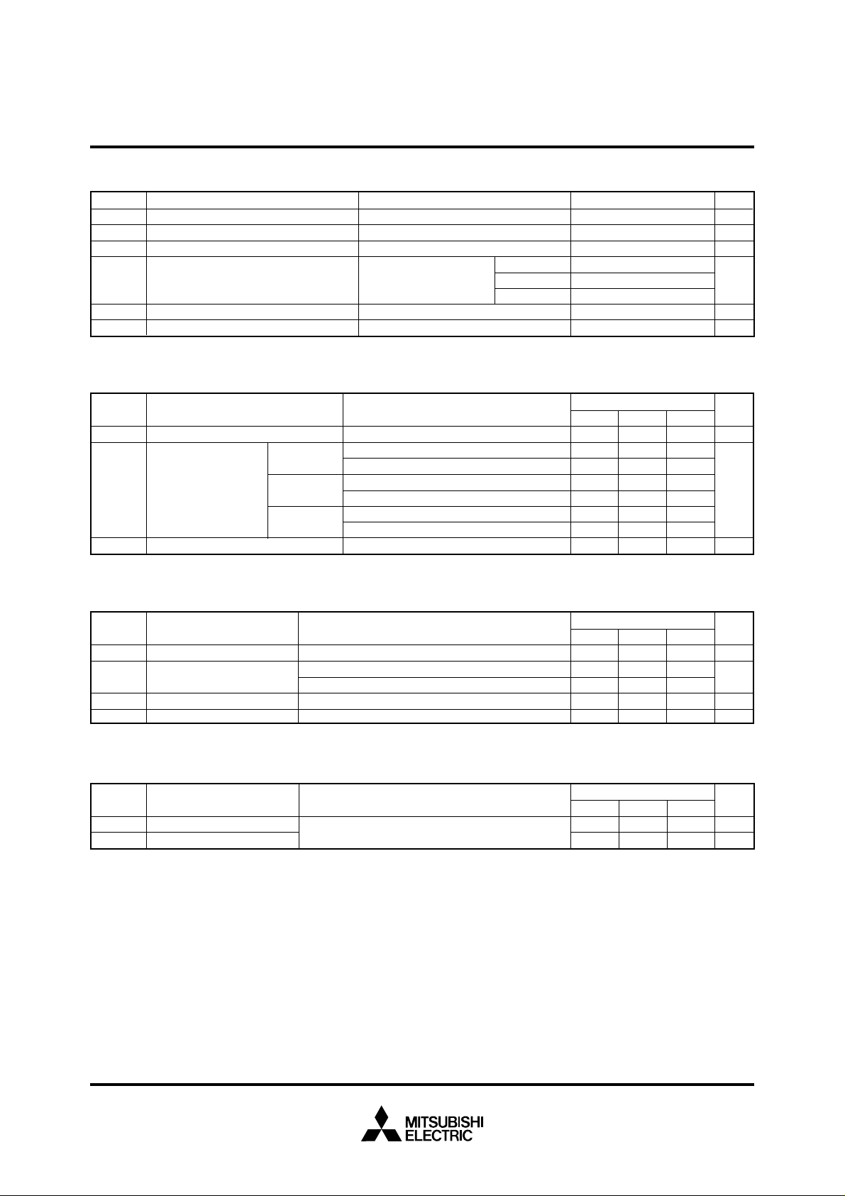
ABSOLUTE MAXIMUM RATINGS (Unless otherwise noted, Ta = –40 ~ +85°C)
VCEO
IC
VI
Pd
Topr
Tstg
Collector-emitter voltage
Collector current
Input voltage
Power dissipation
Operating temperature
Storage temperature
Output, H
Current per circuit output, L
Ta = 25°C, when mounted
on board
RECOMMENDED OPERATING CONDITIONS (Unless otherwise noted, Ta = –40 ~ +85°C)
Symbol UnitParameter Test conditions
VO V0
C
I
VIN Input voltage
Output voltage
Collector current
(Current per 1 circuit when 8 circuits
are coming on simultaneously)
M63807P
M63807FP
M63807KP
Duty Cycle no more than 50%
Duty Cycle no more than 100%
Duty Cycle no more than 30%
Duty Cycle no more than 100%
Duty Cycle no more than 12%
Duty Cycle no more than 100%
8-UNIT 300mA TRANSISTOR ARRAY
M63807P
M63807FP
M63807KP
M63807P/FP/KP
RatingsSymbol Parameter Conditions Unit
–0.5 ~ +35
300
–0.5 ~ +35
1.79
1.10
0.68
–40 ~ +85
–55 ~ +125
Limits
min typ max
—
0
0
0
0
0
0
0
—
—
—
—
—
—
—
250
170
250
130
250
100
mA
W
°C
°
35
mA
30
V
V
C
V
ELECTRICAL CHARACTERISTICS (Unless otherwise noted, Ta = 25°C)
Symbol UnitParameter Test conditions
V
(BR) CEO
CE(sat)
V
VIN(on)
hFE
Collector-emitter breakdown voltage
Collector-emitter saturation voltage
“On” input voltage
DC amplification factor
I
CEO = 10µA
IN = 1mA, IC = 10mA
I
IN = 2mA, IC = 150mA
I
IN = 1mA, IC = 10mA
I
V
CE = 10V, IC = 10mA
SWITCHING CHARACTERISTICS (Unless otherwise noted, Ta = 25°C)
Symbol UnitParameter Test conditions
ton
toff
Turn-on time
Turn-off time
CL = 15pF (note 1)
Limits
min typ max
35
—
—
7.5
50
min typ max
—
—
—
—
—
11.0
—
Limits
120
240
—
0.2
0.8
15.0
—
—
—
V
V
V
—
ns
ns
Jan. 2000
Page 3

PRELIMINARY
Notice: This is not a final specification.
Some parametric limits are subject to change.
MITSUBISHI SEMICONDUCTOR <TRANSISTOR ARRAY>
M63807P/FP/KP
8-UNIT 300mA TRANSISTOR ARRAY
NOTE 1 TEST CIRCUIT
INPUT
Measured device
PG
50Ω
(1)Pulse generator (PG) characteristics : PRR = 1kHz,
tw = 10µs, tr = 6ns, tf = 6ns, Zo = 50Ω, V
(2)Input-output conditions : R
(3)Electrostatic capacity C
connections and input capacitance at probes
TYPICAL CHARACTERISTICS
Thermal Derating Factor Characteristics
2.0
M63807P
1.5
M63807FP
1.0
M63807KP
0.5
Power dissipation Pd (W)
Vo
R
L
OUTPUT
L
C
IH
L
= 220Ω, Vo = 35V
L
includes floating capacitance at
= 11V
0.931
0.572
0.354
TIMING DIAGRAM
50%
INPUT
OUTPUT
(mA)
I
Input current I
50%
ton toff
4
3
2
1
50%
50%
Input Characteristics
Ta = –40°C
Ta = 25°C
Ta = 85°C
0
0
25 50 75 10085
Ambient temperature Ta (°C)
Duty Cycle-Collector Characteristics
(M63807P)
400
300
200
•The collector current values
100
Collector current Ic (mA)
represent the current per circuit.
•Repeated frequency ≥ 10Hz
•The value the circle represents the value of
the simultaneously-operated circuit.
•Ta = 25°C
0
20 40 60 80
0
Duty cycle (%)
100
0
030252015105
Input voltage V
I
(V)
Duty Cycle-Collector Characteristics
(M63807P)
400
➀
~
➄
➅
➆
➇
300
200
•The collector current values
100
represent the current per circuit.
Collector current Ic (mA)
•Repeated frequency ≥ 10Hz
•The value the circle represents the value of
the simultaneously-operated circuit.
•Ta = 85°C
0
0
20 40 60 80
100
~
➂
➀
➃
➄
➅
➆
➇
Duty cycle (%)
Jan. 2000
Page 4

PRELIMINARY
Notice: This is not a final specification.
Some parametric limits are subject to change.
MITSUBISHI SEMICONDUCTOR <TRANSISTOR ARRAY>
M63807P/FP/KP
8-UNIT 300mA TRANSISTOR ARRAY
Duty Cycle-Collector Characteristics
400
(M63807FP)
300
200
•The collector current values
100
Collector current Ic (mA)
represent the current per circuit.
•Repeated frequency ≥ 10Hz
•The value the circle represents the value of
the simultaneously-operated circuit.
•Ta = 25°C
0
0
20 40 60 80
Duty cycle (%)
Duty Cycle-Collector Characteristics
400
(M63807KP)
300
200
•The collector current values
100
Collector current Ic (mA)
represent the current per circuit.
•Repeated frequency ≥ 10Hz
•The value the circle represents the value of
the simultaneously-operated circuit.
•Ta = 25°C
0
0
20 40 60 80
100
100
➀~➂
➃
➄
➅
➆
➇
~
➀
➂
➃
➄
➅
➆
➇
Duty Cycle-Collector Characteristics
400
300
(M63807FP)
➀
➁
➂
200
•The collector current values
100
Collector current Ic (mA)
represent the current per circuit.
•Repeated frequency ≥ 10Hz
•The value the circle represents the value of
the simultaneously-operated circuit.
•Ta = 85°C
0
0
20 40 60 80
100
➃
➄
➅
➆
➇
Duty cycle (%)
Duty Cycle-Collector Characteristics
(M63807KP)
400
➁
300
200
➀
➁
➂
➃
➄
100
➅
➆
➇
•The collector current values
100
Collector current Ic (mA)
represent the current per circuit.
•Repeated frequency ≥ 10Hz
•The value the circle represents the value of
the simultaneously-operated circuit.
•Ta = 85°C
0
0
20 40 60 80
Duty cycle (%)
Output Saturation Voltage
Collector Current Characteristics
250
200
Ta = 25°C
I
B
= 3mA
B
= 2mA
I
150
100
I
Collector current Ic (mA)
50
0
0 0.2 0.4 0.6 0.8
Output saturation voltage V
I
B
I
B
= 1mA
B
= 0.5mA
CE(sat)
= 1.5mA
(V)
Duty cycle (%)
Output Saturation Voltage
Collector Current Characteristics
100
Ta = 25°C
80
V
V
I
I
= 28V
= 24V
60
40
20
Collector current Ic (mA)
0
0 0.05 0.10 0.15 0.20
Output saturation voltage V
I
V
V
I
I
= 16V
V
= 12V
= 8V
CE(sat)
I
V
= 20V
(V)
Jan. 2000
Page 5

PRELIMINARY
Notice: This is not a final specification.
Some parametric limits are subject to change.
MITSUBISHI SEMICONDUCTOR <TRANSISTOR ARRAY>
M63807P/FP/KP
8-UNIT 300mA TRANSISTOR ARRAY
Output Saturation Voltage
Collector Current Characteristics
100
II = 2mA
80
Ta = –40°C
60
40
20
Collector current Ic (mA)
0
0 0.05 0.10 0.15 0.20
Output saturation voltage V
Grounded Emitter Transfer Characteristics
50
VCE = 4V
40
30
Ta = 85°C
Ta = 25°C
Ta = 85°C
CE(sat)
(V)
Ta = –40°C
DC Amplification Factor
Collector Current Characteristics
3
10
V
CE
10V
7
Ta = 25°C
5
FE
3
2
2
10
7
5
3
DC amplification factor h
2
1
10
0
10
2357 2357
10
1
Collector current Ic (mA)
Grounded Emitter Transfer Characteristics
250
VCE = 4V
Ta = 85°C
200
150
Ta = 25°C
10
2
23 57
10
3
20
Collector current Ic (mA)
10
0
0 1.0 2.0 3.0 4.0 5.0
Input voltage V
Ta = 25°C
I
(V)
100
Collector current Ic (mA)
50
0
048121620
Ta = –40°C
Input voltage V
I
(V)
Jan. 2000
 Loading...