

Page 1
MITSUBISHI SEMICONDUCTOR <TRANSISTOR ARRAY>
M63800FP
7-UNIT 500mA SOURCE TYPE DARLINGTON TRANSISTOR ARRAY WITH CLAMP DIODE
DESCRIPTION
M63800FP is a seven-circuit output-sourcing Darlington
transistor array. The circuits are made of PNP and NPN transistors. This semiconductor integrated circuit performs highcurrent driving with extremely low input-current supply.
FEATURES
Á High breakdown voltage (BV
CEO ≥ 50V)
Á High-current driving (Io(max) = –500mA)
Á With output clamping diodes
Á
Driving available with CMOS IC output of 6-16V or with TTL output
Á Wide operating temperature range (Ta = –20 to +75°C)
Á Output current-sourcing type
APPLICATION
Drives of relays, printers, LEDs, fluorescent display tubes
and lamps, and interfaces between MOS-bipolar logic systems and relays, solenoids, or small motors
FUNCTION
The M63800FP has seven circuits, which are made of input
inverters and current-sourcing outputs. The outputs are
made of PNP transistors and NPN Darlington transistors.
The PNP transistor base current is constant. A spike-killer
clamping diode is provided between each output pin and
GND. V
S (pin 8) and GND (pin 9) are used commonly among
the eight circuits.
The input has resistance of 3kΩ, and a maximum of 10V can
be applied. The output current is 500mA maximum. Supply
voltage V
S is 50V maximum.
The M63800FP is enclosed in a molded small flat package,
enabling space-saving design.
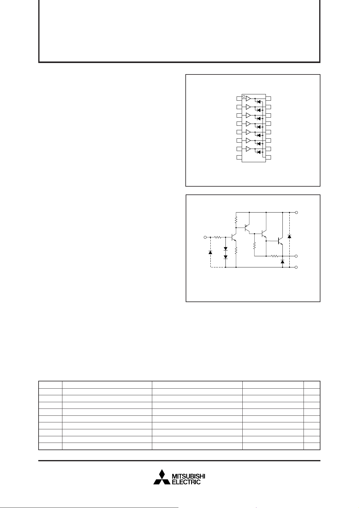
PIN CONFIGURATION
→O1
→O2
→O3
OUTPUT
→O4
→O5
→O6
→O7
9
GNDV
INPUT
IN2→
IN3→
IN4→
IN5→
IN6→
IN7→
S
1IN1→
2
3
4
5
6
7
8
16
15
14
13
12
11
10
Package type 16P2N-A
CIRCUIT DIAGRAM
20K
INPUT
The diode, indicated with the dotted line, is parasitic, and cannot
be used.
3K
7.2K
1.5K
The seven circuits share the V
3K
S
and GND.
S
V
OUTPUT
GND
Unit : Ω
ABSOLUTE MAXIMUM RATINGS (Unless otherwise noted, Ta = –20 ~ +75°C)
#
VCEO
VS
VI
IO
IF
VR
Pd
Topr
Tstg
# : Unused I/O pins must be connected to GND.
Collector-emitter voltage
Supply voltage
Input voltage
Output current
Clamping diode forward current
#
Clamping diode reverse voltage
Power dissipation
Operating temperature
Storage temperature
Output, L
Current per circuit output, H
Ta = 25°C, when mounted on board
RatingsSymbol Parameter Conditions
–0.5 ~ +50
50
–0.5 ~ +10
–500
–500
50
1.00
–20 ~ +75
–55 ~ +125
Unit
V
V
V
mA
mA
V
W
°C
°C
Aug. 1999
Page 2
MITSUBISHI SEMICONDUCTOR <TRANSISTOR ARRAY>
M63800FP
7-UNIT 500mA SOURCE TYPE DARLINGTON TRANSISTOR ARRAY WITH CLAMP DIODE
RECOMMENDED OPERATING CONDITIONS (Unless otherwise noted, Ta = –20 ~ +75°C)
2.4
Limits
—
0
0
—
–350
50
V
mA
0
—
–100
5
—
0
0.2
10
V
V
Limits
+
1.6
0.6
2.9
5.6
max
100
2.4
2.0
1.0
5.0
15.0
–2.4
100
µA
V
mA
mA
V
µA
min typ
—
—
—
1.45
—
—
—
—
–1.2
—
—
—
Symbol Unit
S
V
Supply voltage
Output current
IO
(Current per 1 circuit when 7 circuits
are coming on si-
multaneously)
VIH
VIL
“H” input voltage
“L” input voltage
Parameter
Duty Cycle
no more than 7%
Duty Cycle
no more than 40%
min typ max
ELECTRICAL CHARACTERISTICS (Unless otherwise noted, Ta = –20 ~ +75°C)
Symbol UnitParameter Test conditions
#
IS (leak)
V
CE (sat)
II
IS
VF
IR
+ : The typical values are those measured under ambient temperature (Ta) of 25°C. There is no guarantee that these values are obtained under any
conditions.
# : Unused I/O pins must be connected to GND.
Supply leak current
Collector-emitter saturation voltage
Input current
Supply current
Clamping diode forward voltage
#
Clamping diode reverse current
VS = 50V, VI = 0.2V
S = 10V, VI = 2.4V , IO = –350mA
V
S = 10V, VI = 2.4V , IO = –100mA
V
I = 3V
V
I = 10V
V
S = 50V, VI = 3V (all input)
V
F = –350mA
I
R = 50V
V
SWITCHING CHARACTERISTICS (Unless otherwise noted, Ta = 25°C)
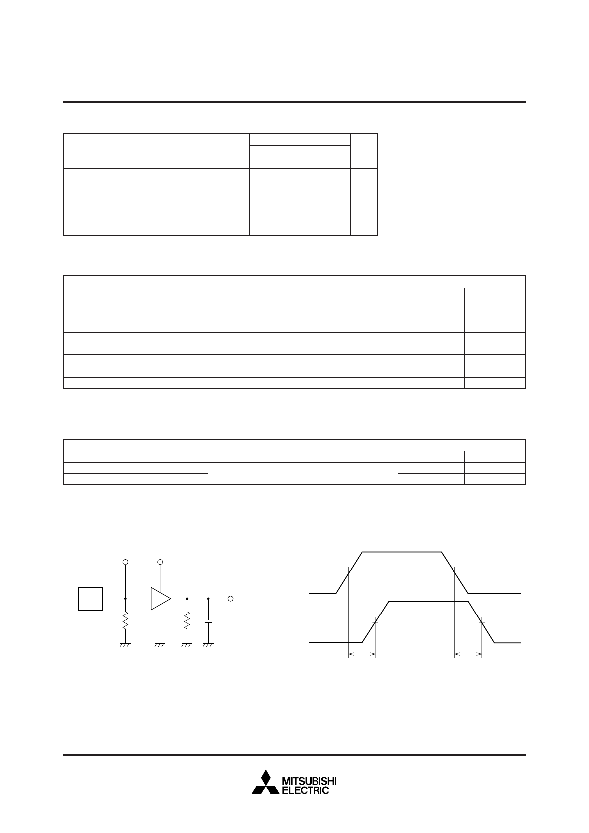
Symbol UnitParameter Test conditions
ton
toff
Turn-on time
Turn-off time
C
L = 15pF (note 1)
TIMING DIAGRAMNOTE 1 TEST CIRCUIT
V
INPUT
PG
50Ω C
(1) Pulse generator (PG) characteristics : PRR = 1kHz,
tw = 10µs, tr = 6ns, tf = 6ns, Z
I
= 0 to 2.4V
V
(2) Input-output conditions : R
(3) Electrostatic capacity C
connections and input capacitance at probes
S
Measured device
OUTPUT
L
R
L
O
= 50Ω
L
= 30Ω, VS = 10V
L
includes floating capacitance at
INPUT
OUTPUT
Limits
min typ max
—
—
50% 50%
50% 50%
ton
100
4800
toff
ns
—
ns
—
Aug. 1999
Page 3

7-UNIT 500mA SOURCE TYPE DARLINGTON TRANSISTOR ARRAY WITH CLAMP DIODE
TYPICAL CHARACTERISTICS
MITSUBISHI SEMICONDUCTOR <TRANSISTOR ARRAY>
M63800FP
Thermal Derating Factor Characteristics
2.0
1.5
1.0
0.5
Power dissipation Pd (W)
0
0
25 50 75 100
Ambient temperature Ta (°C)
Duty-Cycle-Output Current Characteristics
–500
–400
–300
–200
•The output current values
Output current IO (mA)
represent the current per circuit.
–100
•Repeated frequency ≥ 10Hz
•The value in the circle represents the
value of the simultaneously-operated circuit.
•Ta = 25°C
0
0
20 40 60 80 100
Output Saturation Voltage
–500
–400
Output Current Characteristics
VS = 10V
VI = 2.4V
Ta = 75°C
Ta = 25°C
Ta = –20°C
–300
–200
Output current IO (mA)
–100
0
0
0.5 1.0 1.5 2.0 2.5
Output saturation voltage V
CE (sat) (V)
Duty-Cycle-Output Current Characteristics
–500
➀
–400
–300
➀
➁
➂
➃
➄
➅
➆
–200
•The output current values
Output current IO (mA)
–100
represent the current per circuit.
•Repeated frequency ≥ 10Hz
•The value in the circle represents the
value of the simultaneously-operated circuit.
0
0
20 40 60 80 100
•Ta = 75°C
➁
➂
➃
➄
➅
➆
Duty cycle (%)
Duty cycle (%)
Grounded Emitter Transfer Characteristics Clamping Diode Characteristics
–500
–400
–300
–200
Output current IO (mA)
–100
VS = 20V
VS-VO = 4V
Ta = 75°C
Ta = 25°C
Ta = –20°C
0
0
0.2 0.4 0.6 0.8 1.0
Input voltage VI (V)
500
400
Ta = 75°C
Ta = 25°C
Ta = –20°C
300
200
100
Forward bias current IF (mA)
0
0 0.5 1.0 1.5
Forward bias voltage VF (V)
2.0
Aug. 1999
Page 4

MITSUBISHI SEMICONDUCTOR <TRANSISTOR ARRAY>
M63800FP
7-UNIT 500mA SOURCE TYPE DARLINGTON TRANSISTOR ARRAY WITH CLAMP DIODE
1.0
VS = 20V
0.8
(mA)
I
0.6
0.4
Input current I
0.2
0
0
Input Characteristics
Ta = 75°C
Ta = 25°C
Ta = –20°C
12345
Input voltage V
I
(V)
5
4
(mA)
I
3
2
Input current I
1
0
0
Input Characteristics
VS = 20V
Ta = 75°C
Ta = 25°C
Ta = –20°C
246810
Input voltage V
I
(V)
Aug. 1999
 Loading...