

Page 1
MITSUBISHI SEMICONDUCTOR (LSI)
GND
GND
LOIN
MU
LO
RSL
SL
V
RSP
HW
HV
HU
GND
GNDHBFG
TOIN
LOIN
OSC
FO
RTO
OPIN-SPIN
V
VM
M63015FP
SPINDLE MOTOR AND 4CH ACTUATOR DRIVER
DESCRIPTION
This M63015FP is 1 chip driver IC for spindle motor and 4 channel
actuators. All of the motor and actuator of optical disk drive system
(CD-ROM etc.) can be drived by only this IC.
This IC has current control drive system for Focus,Tracking,
Spindle and Slide channel drive, also has a direct PWM control
system for Spindle and Slide channels drive due to reducing IC
power dissipation.
This IC has three voltage supply terminals (for Spindle,
Slide/Loading and Focus/Tracking) , and these voltage supply can
be set separately.
Further more this IC has an operational amplifier for Slide input,
FG amplifier, thermal shut down circuit, standby circuit, channel
select function, reverse rotation detect circuit and Short braking
select.
APPLICATION
CD-ROM, DVD, DVD-ROM, DVD-RAM ,Optical disc related
system, etc.
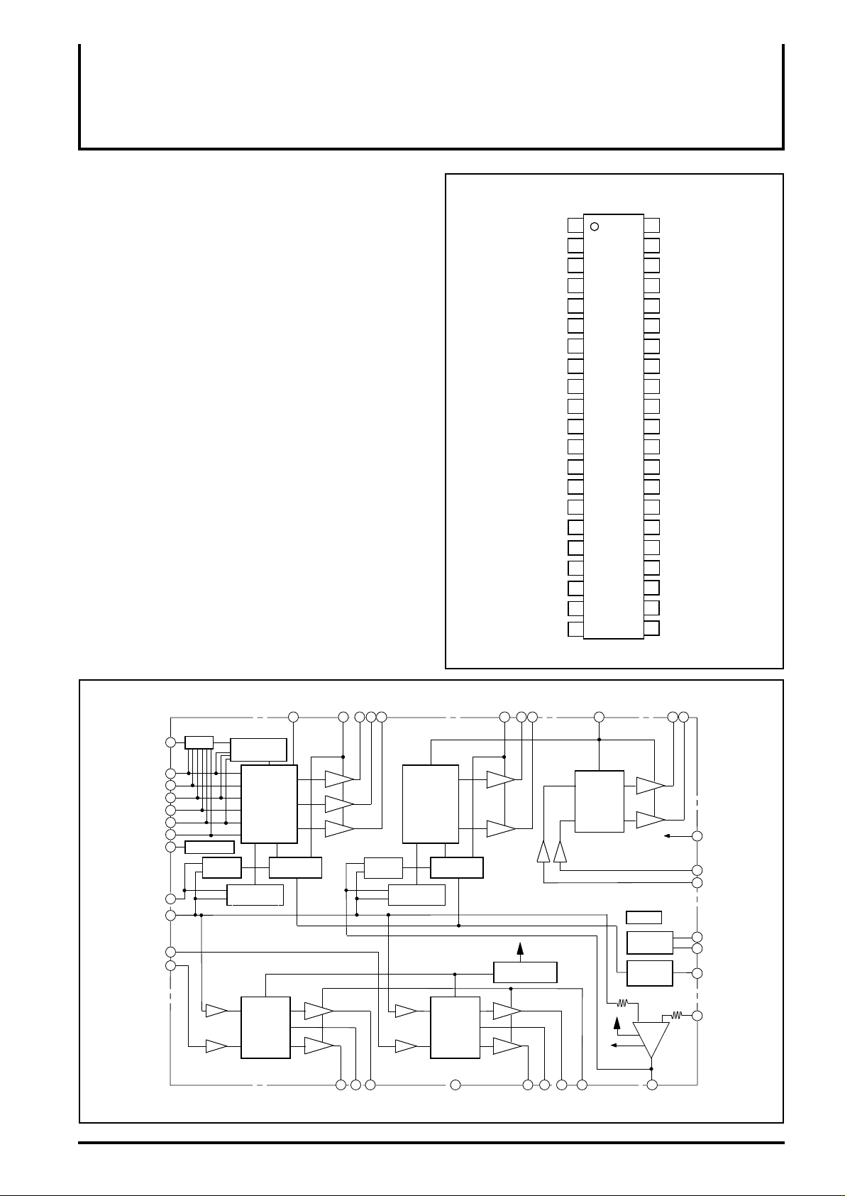
PIN CONFIGURATION (TOP VIEW)
+
1
MU1
2
2
3
VM23
4
+
LO-
7
8
SL+
-
W
13
14
U
15 28
HW-
16
+
17
18
HV-
+
19
HU-
20
21
+
Outline 42P9R-K/B
42
RFO
41
40
5
39
VM4
385
376
TO+
TO-
36
FO-
35
349
M63015FP
3310
SLIN
3211
3112
30
29
FOIN
27
26
REF
25
24
23
22
-
CC
+
1
BLOCK DIAGRAM
FG
HU+
HU-
HV+
HVHW+
HW-
HB
SPIN
REF
TOIN
FOIN
FG
Hall Bias
VM1
s
s
Reverse
Detect
Spindle Slide
Direction
comp.
Focus
Current
comp.
ss
TO+
CTL
amp.
RSPUV
RTO
CTL
amp.
TO-
W
Direction
comp.
Current
comp.
Reg
Tracking
GND
SL+
RSL
VM1
Regulator
FO+
SL-
RFO
FO-
VM23
ss
Loading
VM4
10K
Reg
5VCC
5V power
supply
TSD
BIAS
Frequency
generator
+ -
SLIN
2 K
LO+
LO-
5VCC
LOIN+
LOIN-
MU1
MU2
OSC
OPIN-
Page 2
C
DESCRIPTIN OF PIN
O
lifi
M
Slide/Loading)
M
TS)
C
N
Pin No.
1
2
3
4
5
6
7
8
9
10
11
12
13
14
15
16
17
18
19
20
21
Symbol
LOIN+
MU1
MU2
VM23
LO+
LOGND
RSL
SL+
SLGND
W
V
U
RSP
HW-
HW+
HV-
HV+
HUHU+
SPINDLE MOTOR AND 4CH ACTUATOR DRIVER
Function
Loading control input(+)
mute 1
mute 2
otor Power Suppry 3(for
Loading non-inverted output
Loading inverted output
GND
Slide current sense
Slide non-inverted output 34
Slide inverted output
GND 32
Motor drive output W
Motor drive output V 30
Motor drive output U
Spindle current sensie
HW- sensor amp. input
HW+ sensor amp. input
HV- sensor amp. input
HV+ sensor amp. input
HU- sensor amp. input
HU+ sensor amp. input
Pin No. Symbol Function
42
41
40
39
38
37
36
35
33
31
29
28
27
26
25
24
23
22
MITSUBISHI SEMICONDUCTOR (LSI)
M63015FP
LOINRFO
RTO
5VCC 5V Power Suppry
VM4
TO+
TOFOFO+
GND
SLIN
OPINOSC
GND
FOIN
TOIN
SPIN
REF
FG
HB
VM1
Loading control input(-)
urrent feedback terminal for Focus
urrent feedback terminal for Tracking
otor Power Suppry 4(for FS and
Tracking non-inverted output
Tracking inverted output
Focus inverted output
Focus non-inverted output
GND
Slide control input
perational amp
er imverted input
PWM carrier oscilation set
GND
Focus control voltage input
Tracking control voltage input
Spindle control voltage input
Reference voltage input
Frequency generator output
Bias for Hall Sensor
Motor Power Suppry 1(for Spindle)
ABSOLUTE MAXIMUM RATINGS (Ta=25˚C, unless otherwise noted)
Symbol
5VCC
VM1
VM23
VM4
IoA
IoB
IoC
5V power supply
Motor power supply 1
Motor power supply 23
Motor power supply 4
Motor output current A 1.5
Motor output current B
Motor output current C 1.0
Maximum input voltage of terminals
Pt
Kq
T
j
opr
T
Tstg
ote 1 : The ICs must be operated within the Pt (power dissipation) or the area of safety operation.
Power dissipation 2.6
Thermal derating 20.8
Junction temperature 150
Operating temperature -20~+75
Storage temperature -40~+150
Parameter
Conditions
Spindle power supply
Slide and loading power supply
Focus and tracking power supply
Spindle output current Note1
Slide output current Note1
Focus,Tracking and Loading output current Note1
MU1,MU2,Hw-,Hw+,Hv-,Hv+,Hu-,Hu+,REF,SPIN,
TOIN, FOIN, OSC,OPIN-,LOIN-,LOIN+
Free air and on the grass epoxy board 70mmX70mmX1.6mm
Free air and on the grass epoxy board 70mmX70mmX1.6mm
RECOMMENDED OPERATING CONDITIONS (Ta=25˚C, unless otherwise noted)
Symbol UnitParameter
VM1
VM23
VM4
IoA
IoB
Fosc
VM1 power supply (forspindle)
VM23 power supply (for slide and loading)
VM4 power supply (for focus and tracking)
Spindle and slide output current Note 2
Focus, tracking and loading output current
Focus, tracking and loading output current
Limits
min. typ. max.
6 13.2
12
4.5 13.2 V12
4.5
–
–
30
0.5
–
5
13.2
1.0
0.8
120 kHz
V
V
A
A0.5
Ratings
7
15
15
15
1.0
CC
0~5V
Unit
V
V
V
V
A
A
A
VVin
W
mW/˚C
˚C
˚C
˚C
Page 3

TYPICAL CHARACTERISTICS
This IC'
POWER-SSOP
6.0
5.0
4.0
3.0
2.0
1.0
POWER DISSIPATION (Pdp)W
Using N-type board:3.6W
Using P-type,O-type
board:2.6W
MITSUBISHI SEMICONDUCTOR (LSI)
M63015FP
SPINDLE MOTOR AND 4CH ACTUATOR DRIVER
s package is
improving the board on which the IC is
mounted enables a large power dissipation
without a heat sink.
For example, using an 1 layer glass epoxy
resin board, the IC's power dissipation is
2.6W at least. And it comes to 3.6W by
using an improved 2 layer board.
The information of the N, P, O type board is
shown in attached.
, so
0
0
25
50 100
75
125 150
AMBIENT TEMPERATURE Ta (˚C)
ELECTRICAL CHARACTERISTICS (Ta=25˚C, 5VCC=VM4=5V,VM1=VM23=12V unless otherwise noted.)
Parameter Test conditionsSymbol
Common
Icc1
Icc2
Fosc
VinOP
IinOP
VofOP
VoutOP
VinREF
IinREF
VMULO
VMUHI
IMU
Spindle
Vdyc1
Vdead1Vdead1+
Vin1
Gvo1
Vlim1F
Vlim1R
VHcom
VHmin
VHB
IHB
FGD
Slide
Vdyc2
Vdead2-
Vdead2+
Vin2
Gvo2
Vlim2
Tdon
Tdoff
Tdsw
Ileak
Supply current
Sleep current
PWM carrier frequency
OPamp input voltage range
OPamp input current
OPamp input offset voltage
OPamp output voltage range
REF input voltage range
REF input voltage range
MUTE terminal low voltage 0.8 V
MUTE terminal high voltage V
Mute terminal input current
Dynamic range of output V
Control voltage dead zone1
Control voltage input range 1 5V
Control gain 1 1.15
Control limit 1F
Control limit 1R 0.41 V
Hall sensor amp.common mode input range
Hall sensor amp.input signal level
HB output voltage 1.2 V
HB terminal sink current 30 mV
FG duty 30 mV
Dynamic range of output
Control voltage dead zone 2
Control voltage input range 2
Control gain 2
Control limit 2 0.58 V
Output turn-on delay 2.0
Output turn-off delay
Output switching delay 10.0 µsec
Output leak current 100
5VCC,VM1, VM23, VM4 current
5VCC,VM1, VM23, VM4 current under Sleep (MU1 = MU2 =0V).
OSC : with 180pF
OPINOPIN-=1.65V
REF=1.65V(OPIN-=OPOUT ;buffer)
Io=-2.0~+2.0mA
VREF=1.65V
MU1,MU2
MU1,MU2
MU1,MU2 at 5V input voltage
Io=0.5 [A]
SPIN<REF [REVERSE]
REF<SPIN [FORWARD]
SPIN
Ilim1F=Vlim1F/ Rs [A] [FORWARD]
Ilim1R=Vlim1R/ Rs [A] [REVERSE]
Hu+,Hu-,Hv+,Hv-,Hw+ ,Hwat Load current (IHB)=10mA
MU1=MU2=0V or MU1=MU2=5V orMU1=5V/MU2=0V
at FG frequency=3kHz,hall input signal level 80mVp-p
Io=0.5 [A]
at VM23=5[V]
at VM23=12[V]
SLIN < REF
REF < SLIN
SLIN
Gio2=Gvo2/ Rs [A/V]
Ilim2=Vlim2/ Rs [A]
The time taken to turn on the output after the Rs voltage goes above the
command value.
The time taken to turn off the output after the Rs voltage goes down the
command value.
The time when all the output Tr.s are turned off during the switching of the
output Tr.
-0
-1.0
-10
0.5
1.0
-10
3.0
10.3
-80
0
0
0.85
0.4
0.27
1.3
60
0.6
3.3
10.3
-80
0
0
0.85
0.43
-100
Limits
Typ. Max.Min.
60
110
-0.15
10.8
-40
+40
1.0
0.5
0.34
0.85
3.8
10.8
-40
+40
1.0
0.5
1.0
3.5
5.0
Unit
78
mA
30
µA
KHz
5
V
0
µA
+10
4.5
mV
V
3.3 V
+10 µA
500 µA
0mV
+80 mV
V/VGio1=Gvo1/ Rs [A/V]
0.6 V
3.7
VHu+,Hu-,Hv+,Hv-,Hw+ ,Hw-
mVp-p
V
0mV
+80 mV
5V
1.15 V/V
µsec
7.0 µsec
µAMU1=MU2=5v,MU1=MU2=0v
Page 4
MITSUBISHI SEMICONDUCTOR (LSI)
r
M63015FP
SPINDLE MOTOR AND 4CH ACTUATOR DRIVER
ELECTRICAL CHARACTERISTICS (Ta=25˚C, 5VCC=VM4=5V,VM1=VM23=12V unless otherwise noted.)(cont.)
3.3
10.3
16.6
-100
-50
3.8
6.8
-6.7
Limits
Typ. Max.Min.
3.8
10.8
0
18
0
0
4.2
7.6
0
-8.0
0-5
Loading
Vdyc3
Vin3
Gvo3
Voff1
Focus/Tracking
Vdyc4
Vin4
Gvo4
Voff 2
Dynamic range of output V
Control voltage input range3
Control gain 3
Output offset voltage
Dynamic range of output
Control voltage input range 4
Control gain 4
Output offset voltage
Parameter Test conditionsSymbol
Io=0.5[A]
LOIN+,LOIN-
(LO+) - (LO-)
(LOIN+) - (LOIN-)
(LO+) - (LO-)
Io=0.5[A]
VM1=12[V]
FOIN,TOIN
RFO (RTO)-FO-(TO-)
FOIN(TOIN)-REF
RFO (RTO)-FO-(TO-) at REF=FOIN(TOIN)=1.65V
VM23=5[V]
VM23=12[V]
LOIN+=LOIN-=5V
LOIN+=LOIN-=1.65V
VM4=5[V]
VM4=12[V]
5
19.3
+100
+50
5
-9.4 dB
+5
Unit
V
dB
mV
mV
V
V
mV
THERMAL CHARACTERISTICS
ParameterSymbol
Thermal shut downTSD
● Channel select function
Logic control Drive channel Brake select
MU1 MU2
SELECT4
SELECT3
SELECT2
SELECT1
This IC has two MUTE terminal (MU1 and MU2).
It is possible to control ON / OFF of each channel by external logic
inputs.
It has four kinds of function for select.In case of SELECT1, the bias
of all circuit becomes OFF.
Therefore, this mode is available in order to reduce the powe
dissipation when the waiting mode.
In case of SELECT2,it is possible to select the PWM reverse
braking to take the brake of Spindle motor.
H
L
H
L
H
H
L
L
Loading Slide Focus Tracking Spindle Opamp
On
On
On
Off
On
Off
On
Off
Function starttemperatureofic
Typ. Max.Min.
On
On
On
Off
Also,in case of SELECT4,it is possible to select the short braking
when in the same.
In case of SELECT3,it is possible to do OFF the slide channel.
Regard with making OFF the loading channel in case of
SELECT2,SELECT3 and SELECT4,please refer to
[Loading channel].
On
On
On
Off
Function stop temperature of ic
Typ. Max.Min.
130160 ˚C
On
On
On
Off
On
On
On
Off
Unit
(SPIN<REF)
Short
Short
PWM
-
Page 5

● Loading channel
The loading channel is the circuit of BTL voltage drive. This circuit
has the referential input. Output swing is determined with ∆Vin X 8.
Also,it is possible for this channel to use for the slide motor , the
focus coil and the tracking coil.
The input terminal is high impedance. It is possible to do variable a
gain by external resistor.
The output becomes high impedance in case of both input voltage
becomes under 0.5 volts. It is possible for the input terminal to
operate from 0 volts.The following table and diagram show an
application in case of two MCU port and one MCU port for the
loading motor.In case of one MCU port, if use three state port, it is
possible for this channel to have the stop function.
MITSUBISHI SEMICONDUCTOR (LSI)
M63015FP
SPINDLE MOTOR AND 4CH ACTUATOR DRIVER
VM23
Forward
M
Reverse
LOIN+
LOIN-
LOADING
Channel
LO+
+
Vo
-
LO-
LO-
VM23
2
Coil
-
+
LO+
Application.1 (Two port H/L control)
Logic control
P1 P2
5V 5V
05V
5V 0
00
Situation of loading channel Output voltage swing
Short brake --> Stop Vo= 0 [V]
Reverse rotation Vo= - 8X5XR1/(R1+2XR2)
Forward rotation Vo= 8X5XR1/(R1+2XR2)
Off [ High impedance output] Off
Vo
Output
voltage [V]
Gvo = 8 [v/v]
Vo=[LO+]-[LO-]
=8 X([LOIN+]-[LOIN-])
LO+
+
Coil
-
[LOIN+]-[LOIN-] (V)
LO-
Application.2 (One port H/L control)
Logic control
P1
5V
Z
(Hi impedance)
0
Situation of loading channel
Forward rotation
Short brake --> Stop
Reverse rotation
Output voltage swing
Vo=2.5[V] X8X R2
(R1/2)+R2+R3
Vo= 0 [V]
Vo=- 2.5[V] X8X R2
(R1/2)+R2+R3
Page 6

MITSUBISHI SEMICONDUCTOR (LSI)
REF
SPIN
RSP
R
R
CTL
VM1R
M
Rh5V
F
R
M63015FP
SPINDLE MOTOR AND 4CH ACTUATOR DRIVER
P1
5v
P1
0v
P2
application.1
( Two port H/L control)
5v
0v
P2
R2
R1
R2
LOIN+
LOIN-
● Spindle channel
The relationship between the differential voltage between SPIN
and REF and the torque is shown in right Figure. The voltage
gain[Gvo] is 1.0 [V/V].
The current gain[Gio] is 2.0A/V (at sensing resistor : 0.5 ohm,and
R1=∞,R2=0ohm) in forward torque directions, and the dead zone is
from 0mV to 80mV (at R1=∞,R2=0ohm) .
The coil current gain under the reverse torque is the same with in
forward torque directions.And the limitation function gets on when
the differential voltage of VM1(12V)~RSP is 0.5V at forward and
0.3V at reverse.
Therefore current-gain-control and current-limit of this IC is
determined with sensing resister value, and more detail control
can be determined with setting a gain-resister outer this IC as
below.
5v
Z
P1
0v
application.2
(One port H/Z/L control)
Current limit
Dead zone
Gio
P1
lim1F
IL(A)
R2R3
orward Torque
Dead zone
lim1R
Current limit
5V
R1
LOIN+
LOIN-
R1
Gio
CTL -REF (V)
The example of current-gain and current-limit of spindle
Gio* [A/V]
[A]
1.00
0.66
0.50
Ilim1R
[A]
R1=∞
R2=0 ohm
R1=R2
1.00
1.33
0.66
0.50
Gio*= R1 / [(R1+R2)•Rs] [A/V]
R1=2•R2
0.66
0.44
0.33
2
1.65v
Rs [Ω]
Ilim1F
0.50 0.68 2.00
0.75 0.45
1.00 0.34 1.00
everse torque
s
HB
HU+
HU-
HV+
GND
HV-
HW+
HW-
U
V
W
1
Page 7

MITSUBISHI SEMICONDUCTOR (LSI)
CTL
CTL
REF
SLIN
RSL
VM
R
K
K
OPIN
R
R
SLIN
OPIN
R1R2SLIN
OPIN
C1SL+SL
M
R
M63015FP
SPINDLE MOTOR AND 4CH ACTUATOR DRIVER
● Slide channel
The relationship between the differential voltage between SLIN and
REF and the torque is shown in right Figure. The voltage gain[Gvo]
is 1.0 [V/V]. The current gain is 2.0A/V (at sensing resistor : 0.5
ohm and R1=R2) in forward torque directions, and the dead zone
is from 0mV to 60mV (at R1=R2=16kohm).
The coil current gain under the reverse torque is the same with in
forward torque directions.And the limitation function gets on when
the differential voltage of VM23(12V)~RSL is 0.5V.
Therefore current-gain-control and current-limit of this IC is
determined with sensing resister value.In the input part,built-in an
inverted amplifier. It is possible to control more detail by setting
external circuit.
Forward
everse Torque
Gio
Dead zone
Current limit
s
IL (A)
Current limit
23
Dead zone
CTL -REF (V)
Gio
Reverse
1
2
-
-
2
10
-
+
The example of current-gain and current-limit of slide.
Rs [Ω]
Ilim [A]
0.50
0.75 0.66
1.00
1.00
0.50 1.00
Gio* [A/V]
R1=R2
2.00
1.33
2•R1=R2
1.00
0.66
0.50
Gio*= R1 / [(R1+R2)•Rs] [A/V]
Forward
-
GND
The input resisters, the 10kΩ resister to the non-inverted input and,
the 2kΩ resister to the inverted input, are built-in the operational amplifier.
Therefore the composition value of the external input resisters(R1 R2)
should be set 8kΩ because of the compensation for the input offset voltage.
Reverse
Page 8

MITSUBISHI SEMICONDUCTOR (LSI)
M63015FP
SPINDLE MOTOR AND 4CH ACTUATOR DRIVER
● Focus/tracking channel
The focus and tracking channel is the current feedback control
drive of MITSUBISHI original.The focus and tracking is the same
composition.
The relationship between the differential voltage between FOIN
and REF and the output current is shown in right Figure.
The voltage gain is 0.4 [V/V].Therefore, the current gain is 0.8[A/V]
in case of the sensing resistor is 0.5 ohm.
The maximum range of output swing is limited around 7.5 volts,in
case of VM4 is above 10 volts.
Coil
current [A]
FOIN
REF
2.5R
2.5R
VM4
R
R
+
R
FO-
R
R
RFO
R
FO+
Rs
Coil
VM4
2
Rs
Coil
IL=Vrs/Rs
FO-
RFO
-
+
FO+
IL
Gio=1.0A/V
at Rs=0.33 ohm
Vcoil
Vrs
0
-
Output
voltage [V]
Vrs=(RFO - [FO-])
=0.4 X (FOIN - REF)
FOIN - REF (V)
FO+
+
Coil
-
FOIN - REF (V)
RFO
Rs
FO-
Page 9

● Direct PWM operation
M
M
The spindle and the slide channel is controlled by the direct PWM
control.
Also,built-in the current limit circuit. This IC controls the motor
current directly.
MITSUBISHI SEMICONDUCTOR (LSI)
M63015FP
SPINDLE MOTOR AND 4CH ACTUATOR DRIVER
FORWARD Current path timing 1.
Rs
Current path 1
SL+
Current
path 1
SL-
VM23
RSL
GND
Current
path 2
FORWARD Current path timing 2.
SL+
Current path 2
Control value
VM23
Rs
RSL
SL-
GND
Control value
Io=Vrs / Rs
Motor current
carrier period
Time
Page 10

MITSUBISHI SEMICONDUCTOR (LSI)
M63015FP
SPINDLE MOTOR AND 4CH ACTUATOR DRIVER
● PWM carrier frequency setting
PWM carrier frequency is decided by charging and discharging the
capacitor that is connected to OSC terminal outer IC. Examination
of the relationship the capacitor connected to OSC terminal and
PWM carrier frequency is given in following table.
Capacitor [pF]
Carrier Frequency [kHz]
330 220
65 90
Note : This PWM carrier frequency is typ value.
180
110
130
140
110
160
● Recommendation of short brake mode at spindle drive
This IC has two brake mode, PWM-BRAKE-MODE and SHORTBRAKE-MODE. In this IC recommendation, SHORT-BRAKEMODE is superior to PWM-BRAKE-MODE to reducing the power
dissipation and to avoid breaking down of this IC.
(By excessive reverse torque current in braking a motor with
PWM-BRAKE from high-speed-rotation with being excessive BackEMF, this IC could be broken.)
● The relationship between hall-amplifier-input and
output-current-commutation/FG output at spindle
drive
The relationship between the hall elements, the motor output
current and FG output(18pulse/rotation)
are shown in bellow Figure.
Hw+ Hv+ Hu+
Hall
input
● FG function duty at spindle drive
The FG terminal outputs the square pulse signal synchronizing
with the hall inputs (Hu+,Hu-,Hv+, Hv-,Hw+,Hw-) timing. and, the
FG terminal is open-collector output. (cf. FG timing chart on the
previous page)
● FG function duty at spindle drive
FG function DUTY is shown in a below equation at rihgt Figure.
FG DUTY [%] =
Hall
input
FG
output
Ton
Ton + Toff
Hw+ Hv+ Hu+
Ton
Toff
FG pull-up R:10kΩ
FG output voltage:5V
FG output frequency:3kHz
(SPM motor rev 10000rpm)
Hall input signal level : 80mVp-p
5V
FG High voltage threshold:3.2V
FG Low voltage threshold:0.8V
0V
● Phase delay circuit at slide
Phase delay circuit is built in the IC to detect an output spike
current, when the motor current direction is switching.
In switching the motor current direction, Phase delay circuit switchoff all output trangister of H-bridge for 3µsec.
Output
current
FG
output
Hall elements
VUW
+
0
W
U
W
V
U
Forward
SPIN > REF
V
W
U
V
V
U
V
W
W
Outer roter
U
Reverse
SPIN < REF
In this IC, since output tranjister is NPN-type tranjister, motor coil
current (Io) is larger than sensing resistance current about 20mA
(TYP.) according to base current of output tranjister.
Therefore please design output current with consisting these base
current.
● Output current setting at slide
Page 11

I/O circuit
VM
RSP
UVW
GND
MITSUBISHI SEMICONDUCTOR (LSI)
M63015FP
SPINDLE MOTOR AND 4CH ACTUATOR DRIVER
● FOIN,TOIN,SPIN
LOIN+, LOINOPIN-,REF
5VCC
2K
● HB
5VCC
● VM4,FO+,FO-,TO+,TO-
● Hu+,Hu-
Hv+,HvHw+,Hw-
5VCC
2K
● MU1,MU2
5VCC
2K
8K
30K
● FG ● VM1,RSP,U,V,W
5VCC
5VCC
1
10K
● OSC
5VCC
2K
2K
2K
VM1
VM4
FO+
GND
● VM23,RSL,SL+,SL-,LO+,LO-
VM23
RSL
SL+
GND
FO-
SL-
TO+
TO-
LO+ LO-
9Vmax
REG
Page 12

THE BOARDS FOR THERMAL DERATIN
G
EVALUATION
Board material
Glass-epoxy FR-4
Size
70X70mm
thickness
t=1.6mm
1 and 2 layers
material : copper
thickness : t=18µm
N-type
board
[2 layer]
MITSUBISHI SEMICONDUCTOR (LSI)
M63015FP
SPINDLE MOTOR AND 4CH ACTUATOR DRIVER
1st layer [TOP view] 2nd layer [BACK view]
POWER-SSOP
O-type
board
[2 layer]
P-type
board
[1 layer]
42P9R-K/B
Heat sink
Lead
mounted IC
Chip
Evaluation board
Page 13

MITSUBISHI SEMICONDUCTOR (LSI)
M63015FP
SPINDLE MOTOR AND 4CH ACTUATOR DRIVER
The notes on designing the layout of the board
This IC has direct PWM controls for the Spindle channel and the
Slide channel drive, therefore the circuits of the IC are influenced
more easily by the PWM switching noise than those have linear
controls. Please refer to the following notes on the ocasion of
designing the layout pattern of the board on which the IC is
mounted.
The bad influence of the PWM noise differs in each board,
therefore please consider the following notes as the reference
materials for designing the board.
Note 1
It is necessary for some application in order to reduce the PWM
noise that pass condensers are connected between power supply
pins(VM23:4pin, VM1:22pin, VM4:38 pin, 5VCC:39pin) and GND
pin, even if the power supplies of the application already have pass
condensers. The closer the connection points of the condensers
are to the pins, the more effective it is to reduce the noise.
Please refer to the values of the condensers on the page of [An
example of the values of the external parts.
(The value of the condensors is only a reference value. It differs in
each application because the bad influence of PWM noise relates
to the layout pattern of the board.)
Note 5
The closer the GND side of the capacitor connected with OSC pin
(30 pin) is to the GND pin(33pin), which is the nearest GND to the
GND of the small signal circuit inside the IC, the less the bad
influence of the PWM noise on the GND line comes to be.
cf. [application circuit]
Note 2
The feedback point of the Spindle channel [the Slide channel] is
the connected point to the VM1(22pin) [the VM23(4pin)] line from
the RSP(15pin) [RSL(8pin)] pin through the sensing resistor
RSP[RSL]. Therefore the closer the feedback point is to the power
supply pin, the more stable the circuits are for the PWM noise.
cf. [application circuit]
Note 3
The farther the large current output lines(especially PWM output
lines of the Spindle CH. and the Slide CH.) which are indicated as
wide lines in the Fig. [application circuit] are to the small signal
input lines, the less the bad influence of the PWM noise comes to
be without the cross-talk between a large current output line and a
small input signal line.
Note 4
In case the PWM switching noise influences the REF input, it is
necessary for some application that a condenser is connected
between REF pin(25pin) and GND pin. The closer the connection
points of the condensers are to the pins, the more effective it is to
reduce the noise. (This is the same as note1.)
cf.[application circuit], [An example of the values of the external
parts]
Page 14

APPLICATION EXAMPLE
MITSUBISHI SEMICONDUCTOR (LSI)
M63015FP
SPINDLE MOTOR AND 4CH ACTUATOR DRIVER
5 ~12v
Slide, Loading
M
M
Loading
SLIDE
M
note2
RSP
RSL
R6
R2
R7
MCU
5V
5V
TS
FS
C1
DSP
6v~12v
C3
note5
RTO
C3
C3
10K
*Pull-up
Resistance
R9
R9
RFO
C3
R8
LOIN+
1
MU1
2
MU2
3
VM23
4
LO+
5
6
LOGND
7
RSL
8
SL+
9
+
C5
C4
+
SL-
10
GND
11
12
W
13
V
14
U
RSP
15
16
HW-
17
HW+
18
HVHV+
19
20
HU-
21
HU+
M63015FP
LOIN-
RFO
RTO
5VCC
VM4
TO+
TOFO-
FO+
GND
SLIN
OPIN-
OSC
GND
FOIN
TOIN
SPIN
REF
FG
HB
VM1
R10
42
41
40
39
38
37
36
35
34
33
32
31
30
29
28
27
26
25
24
23
22
+
C2
1.65v
+
C7
C6
C8
C9
R5
R3 R4
R1
note2
Rh
An example of the values of the external parts
These values are only examples, not the guaranteed values. And the values differ in each application.
External parts name
RSP
RSL
RFO, RTO
Rh
R1,R2,R3,R4,R5,R6
R7, R8
R9, R10
C1
C2
C3
C4,C5,C6,C7
C8
Typ.value
0.33
0.5
0.33
200
10
10
10
330
180
0.1-0.01
10-33
0.1
C9 470 pF
Unit
Ω
Ω
Ω
Ω
kΩ
kΩ
kΩ
pF
pF
µF
µF
µF
Note
Ilim1F=1.5[A], Ilim1R=1.0[A], Gain=3.0[A/V]
Ilim=1.0[A], Gain=2.0[A/V]
Gain=1.2[A/V]
Fosc=110kHz
Capacitors against output oscillation in a cold atomosphere.
(The capacitors are not necessary in some application)
Pass condenser for power supply Note 1
REF input noise filter condenser
(The capacitors are not necessary in some application) Note 4
FG output noise filter condenser
(The capacitors are not necessary in some application)
Page 15

PACKAGE OUTLINE
MITSUBISHI SEMICONDUCTOR (LSI)
M63015FP
SPINDLE MOTOR AND 4CH ACTUATOR DRIVER
42P9R-B
HSSOP42-P-450-0.8
E
HE
G
Z1
Lead MaterialWeight(g)JEDEC CodeEIAJ Package Code
Cu Alloy
42
1
D
e
y
z
Detail G
22
F
21
b
A
A2
A1
M
X
L1
Detail F
L
C
e1
Recommended Mount Pad
Symbol
A
1
A
A2
b
c
D
E
e
HE
L
1
L
z
Z1
x
y
b2
e1
l2
e
b2
l2
Dimension in Millimeters
Min Nom Max
—
—
0.27
0.23
17.3
8.2
—
11.63
0.3
—
—
—
—
——
0
—
——
1.27
—
0.10
2.0
0.32
0.25
17.5
8.4
0.8
11.93
0.5
1.765
0.75
—
—
—
¡
0.5
11.43
——
2.2
0.2
—
0.37
0.3
17.7
8.6
—
12.23
0.7
—
—
0.9
0.16
0.1
10
—
¡
Plastic 42pin 450mil HSSOP
 Loading...