

Page 1
M63013FP
Preliminary
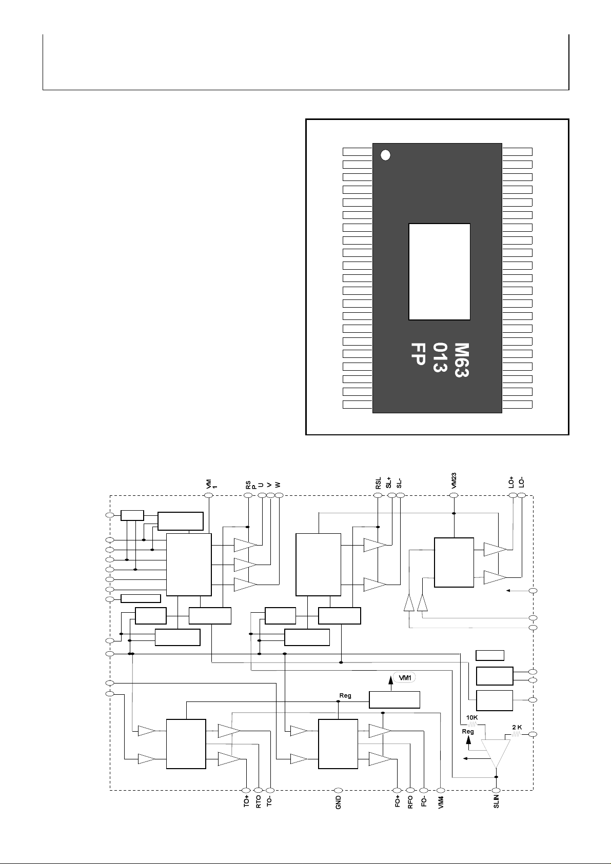
PIN CONFIGURATION
(Top View)
Package outline : 42 PIN POWER SSOP (42P9R-B)
123456789101112131415161718192021
GND
GND
LOIN+
MU2
LO+
RSL
SL-
VURSP
HW+
HV+
HU+
This IC is 1 chip driver IC for spindle motor and 4 channel
actuators. All of the motor and actuator of optical disk drive
system (CD-ROM etc.) can be drived by only this IC.
This IC has current control drive system for Focus, Tracking,
Spindle and Slide channel drive, also has a direct PWM
control system for Spindle and Slide channels drive due to
reducing IC power dissipation.
This IC has three voltage supply terminals (for Spindle,
Slide/Loading and Focus/Tracking) , and these voltage
supply can be set separately.
Further more this IC has an operational amplifier for Slide
input, FG amplifier, thermal shut down circuit, standby circuit,
channel select function, reverse rotation detect circuit and
Short braking select.
252627282930313233343536373839404142222324
GND
GNDHBFG
TOIN
LOIN-
OSC
FO+
RTO
OPIN-
SPIN
5VCC
VM1
FG
Reverse
Detect
CTL
amp.
Frequency
generator
Direction
comp.
CTL
amp.
Direction
comp.
Hall Bias
Regulator
BIAS
TSD
FG
HU+
HU-
HV+
HV-
HW+
HW-HBREF
SPIN
TOIN
FOIN
OPIN-
OSC
MU2
MU1
+ -
sssss
s
5VCC
LOIN-
5VCC
5Vpower
supply
LOIN+
Current
comp.
Current
comp.
[FEATURES]
MITSUBISHI SEMICONDUCTORS
SPINDLE MOTOR AND 4CH ACTUATOR DRIVER
MU1
VM23
LO-
SL+
W
HW-
HV-
HU-
[APPLICATION]
CD-ROM, DVD, DVD-ROM, DVD-RAM ,Optical disc related system,etc
RFO
VM4
TOTO+
FO-
SLIN
FOIN
REF
[BLOCK DIAGRAM]
Spindle Slide
Focus
Tracking
1
( / 17)
Loading
REV990607
Page 2
M63013FP
Preliminary
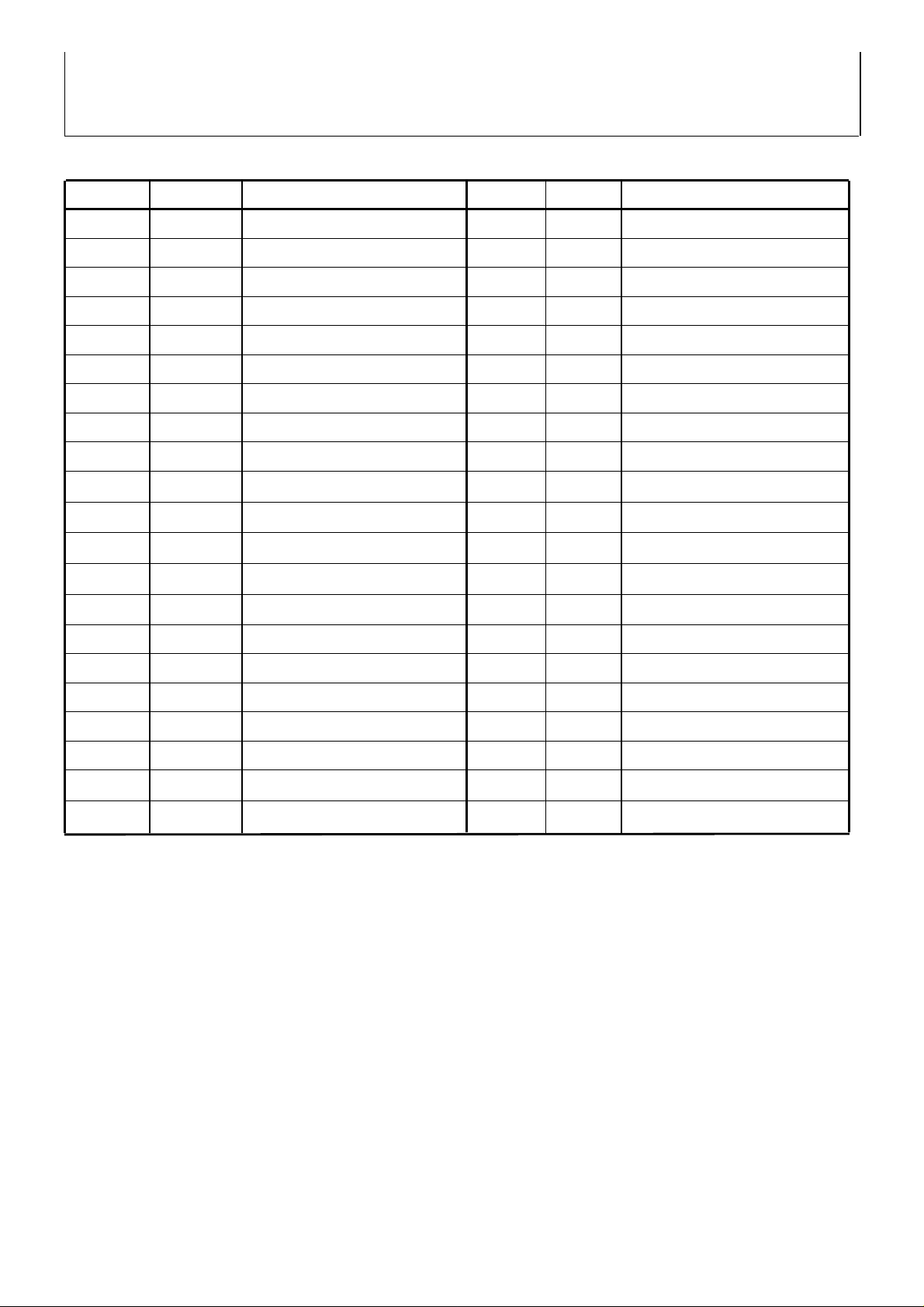
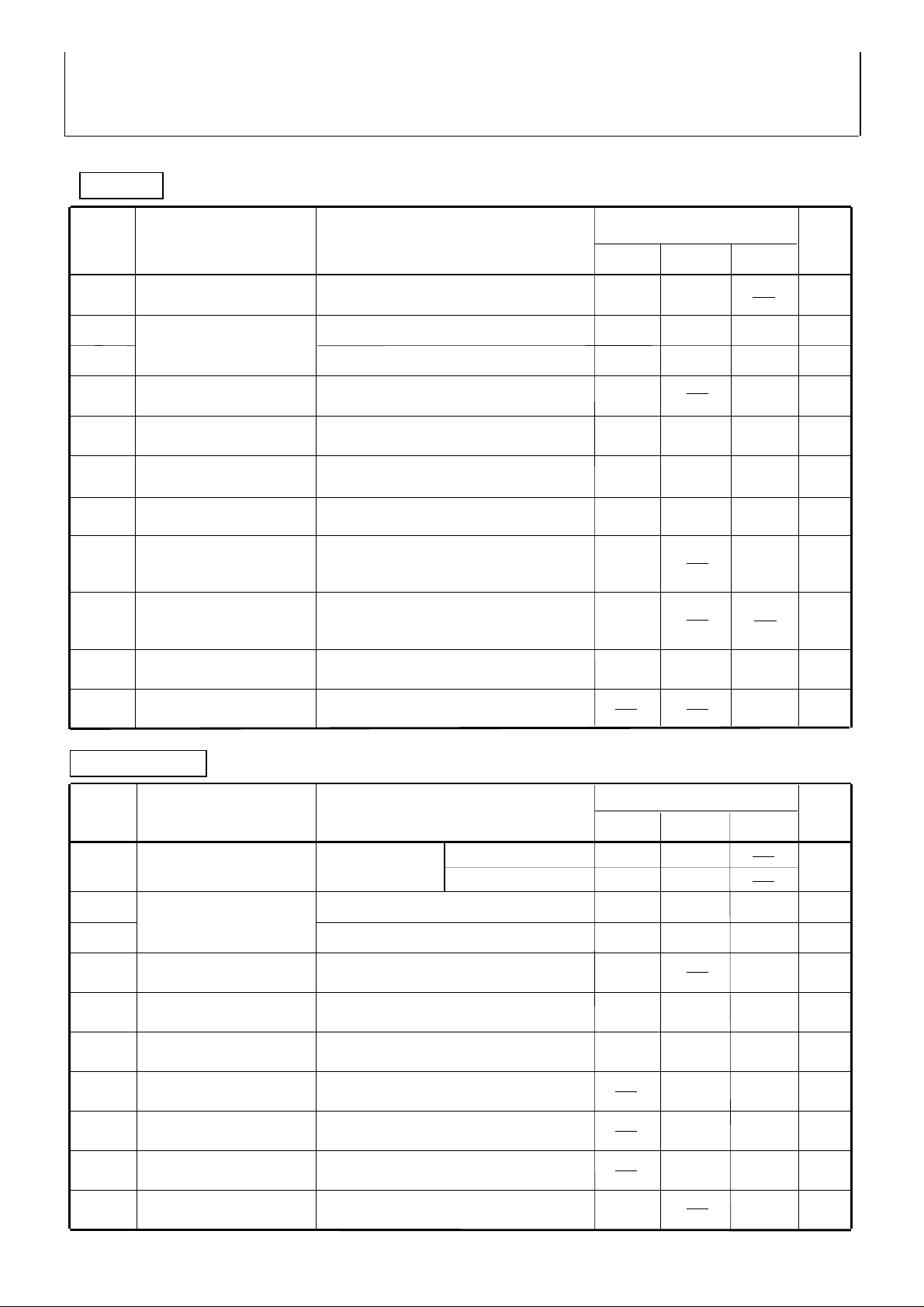
SYMBOL
SYMBOL
TERMINAL
TERMINAL FUNCTION
TERMINAL
TERMINAL FUNCTION
1234567815161718192122232425262728363738394041
42
Loading non-inverted output
LO+
Loading inverted output
LO-
HW-
HW+
HV- sensor amp. input
HV-
RSL
Slide current sense
Motor drive output U
U
Spindle current sensie
RSP
GND
GND
GND
GND1420
29
HW+ sensor amp. input
HW- sensor amp. input
HV+ sensor amp. input
HV+
HU- sensor amp. input
HU-
HU+
HU+ sensor amp. input
35
9
SL+
Slide non-inverted output
34
10
SL-
Slide inverted output
33
GND
GND
11
GND
GND32OPIN-
12
W
Motor drive output W
31
13
V
Motor drive output V
30
MU2
mute 2
mute 1
MU1
VM23
LOIN+
Loading control input(+)
SLIN
Slide control input
SPIN
Tracking control voltage input
PWM carrier oscilation set
OSC
HB
Bias for Hall Sensor
FG
Frequency generator output
FOIN
Focus control voltage input
TOIN
Spindle control voltage input
Focus inverted output
FO-
TO-
Tracking inverted output
TO+
Tracking non-inverted output
VM4
REF
Focus non-inverted output
FO+
Reference voltage input
VM1
Operational amplifier imverted input
Motor Power Suppry 3(for Slide/Loading)
Motor Power Suppry 4(for FS and TS)
Motor Power Suppry 1(for Spindle)
LOIN-
Loading control input(-)
5VCC
5V Power Suppry
RFO
RTO
Current feedback terminal for Focus
Current feedback terminal for Tracking
[PIN FUNCTION]
MITSUBISHI SEMICONDUCTORS
SPINDLE MOTOR AND 4CH ACTUATOR DRIVER
2
( / 17)
REV990607
Page 3
M63013FP
Preliminary
SYMBOL
PARAMETER
CONDITIONS
RATING
Unit
Motor power supply 4
Focus and Tracking power supply
Motor Output Current A
Free Air and on the grass epoxy board
Thermal derating
Operating temperature
Maximum input voltage
*note1 ; The ICs must be operated within the Pt (power dissipation) or the area of safety operation
*note 1
Focus,Tracking and Loading output current
MU1,MU2,Hw-,Hw+,Hv-,Hv+,Hu-,Hu+,REF,
SPIN,TOIN,FOIN,OSC,OPIN-,LOIN-,LOIN+
Free Air and on the grass epoxy board
Motor power supply 1
5V power supply
Motor Output Current B
*note 1
Spindle and Slide output current
with external shottky diode
SYMBOL
PARAMETER
LIMITS
VM1 power supply(for Spindle)
VM4 power supply(for Focus and Tracking)
Spindle and Slide OutputCurrent
Focus, Tracking and Loading Output Current
Motor power supply 2
VM23 power supply(for Slide and Loading)
[ABSOLUTE MAXIMUM RATING] (Ta=25ºC)
MITSUBISHI SEMICONDUCTORS
SPINDLE MOTOR AND 4CH ACTUATOR DRIVER
5VCC
VM1
VM23
Motor power supply 23
Spindle power supply
Slide and Loading power supply
VM4
IoA
IoB
Vin
of terminals
Pt
Power dissipation
Kθ mW / ºC
Tj
Junction temperature
Topr
Tstg
Storage temperature
7
15
15
15
1.2
1.0
0 to 5VCC
2.6
20.8
150
-20 to +75
-40 to +150
V
V
V
V
A
A
V
W
ºC
ºC
ºC
The spindle and slide output terminal is needed external shottky diode between each output and GND
when it is used above 0.6A. Discription(IoA) is case of with external shottky diode.
[RECOMMENDED OPERATING CONDITIONS] (Ta=25ºC )
minimum typical maximum
VM1
VM23 4.5
VM4
IoA
*note2
IoB
*note2
The spindle and slide output terminal is needed external shottky diode between each output and GND
when it is used above 0.6A. Discription(IoA) is case of with external shottky diode.
6
30
12
12
5
0.5
0.5
13.2
13.2
13.24.5
1.0
0.8
120
Unit
V
V
V
A
A
KHzFosc
3
( / 17)
REV990607
Page 4
M63013FP
Preliminary
Ambient Temperature Ta (ºC)
(W)
Icc1
Icc2mAFosc
KHz
5VCC,VM1, VM23, VM4 current
µA
5VCC,VM1, VM23, VM4 current under Sleep
SYMBOL
PARAMETER
Supply current
CONDITIONS
MIN
TYP
MAX
PWM carrier frequency
(MU1 = MU2 =0V)
OSC : with 180pF
VinREF
V
REF input voltage range
VMULO
V
MUTE terminal low voltage
MU1,MU2
VMUHI
V
IMU
µA
Mute terminal input current
at 5V input voltage
IinREF
µA
REF input voltage range
VREF=1.65V
(Ta=25ºC, 5VCC=VM4=5V,VM1=VM23=12V unless otherwise noted.)
VinOP
V5OPamp input voltage range
IinOP
OPamp input current
µA
VofOP
OPamp input offset voltage
VoutOP
V
OPamp output voltage range
MUTE terminal high voltage
MU1,MU2
MU1,MU2
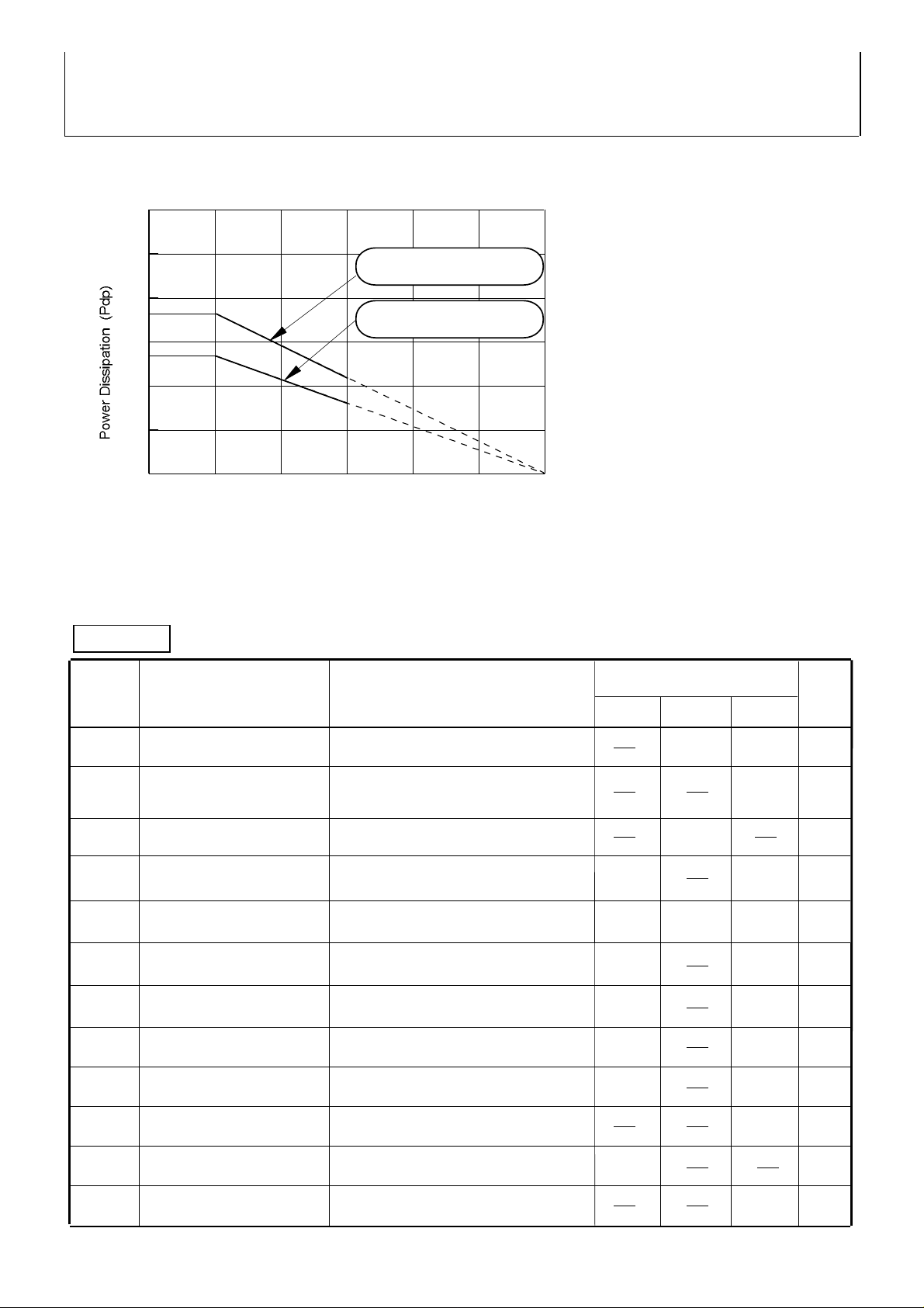
[THERMAL DERATING]
6.0
5.0
4.0
3.0
2.0
1.0
0 25 50 75 100 125 150
SPINDLE MOTOR AND 4CH ACTUATOR DRIVER
3.6W
using N-type board
2.6W
using P-type board
MITSUBISHI SEMICONDUCTORS
This IC's package is POWER-SSOP,
so improving the board on which the IC
is mounted enables a large power
dissipation without a heat sink.
For example, using an 1 layer glass
epoxy resin board, the IC's power
dissipation is 2.6W at least. And it
comes to 3.6W by using an improved 2
layer board.
The information of the N, P type board
is shown in attached.
[ELECTRICAL CHARACTERISTICS]
Common
Sleep current
OPIN-
OPIN-=1.65V
REF=1.65V(OPIN-=OPOUT ;buffer)
-10
0.5Io=-2.0 to +2.0mA
LIMITS
Unit
60
78
30
110
0
0-1.0 -0.15
+10
mV
4.5
4
( / 17)
1.0
-10
3.0
3.3
+10
0.8
500
REV990607
Page 5
M63013FP
Preliminary
Vdyc1
Vdead1-
V
Vin1
V
mV
SYMBOL
PARAMETER
Dynamic range of output
CONDITIONS
LIMITS
MIN
TYP
MAX
Control voltage input range 1
Control voltage dead zone 1
SPIN
Gvo1
V/V
Control gain 1
Gio1=Gvo1/ Rs [A/V]
Vlim1F
V
Control limit 1F
VHmin
mVp-p
VHBVHB output voltage
IHB
mA
HB terminal sink current
VHcom
V
common mode input range
Hall sensor amp.
input signal level
Hall sensor amp.
mV
Vdead1+
SPIN<REF
REF<SPIN
Ilim1F=Vlim1F/ Rs [A]
at Load current (IHB)=10mA
[REVERSE]
[FORWARD]
Hu+,Hu-,Hv+,Hv-,Hw+ ,Hw-
Hu+,Hu-,Hv+,Hv-,Hw+ ,Hw-
(Ta=25ºC, 5VCC=VM4=5V,VM1=VM23=12V unless otherwise noted.)
Vdead2-
V
Vin2
V
mV
SYMBOL
MIN
TYP
MAX
Control voltage input range 2
Control voltage dead zone 2
SLIN
Gvo2
V/V
Control gain 2
Vlim2
V
Control limit 2
Tdon
Output turn-on delay
Tdoff
Output turn-off delay
mV
Vdead2+
SLIN < REF
REF < SLIN
Tdsw
Output switching delay
Ileak
Output leak current
MU1=MU2=5v,MU1=MU2=0v
Vdyc2
Dynamic range of output
(Ta=25ºC, 5VCC=VM4=5V,VM1=VM23=12V unless otherwise noted.)
MU1=MU2=0V or MU1=MU2=5V or
MU1=5V/MU2=0V
at VM23=5[V]
at VM23=12[V]
[REVERSE]
[FORWARD]
Vlim1R
Control limit 1R
Ilim1R=Vlim1R/ Rs [A]
V
[ELECTRICAL CHARACTERISTICS]
Spindle
MITSUBISHI SEMICONDUCTORS
SPINDLE MOTOR AND 4CH ACTUATOR DRIVER
Unit
Io=0.5 [A]
-80
0
0.85
0.4
1.3
60
10.810.3
-40
+40
+80
50
1.0 1.15
0.5
0.410.27 0.34
3.7
1.20.6 0.85
30
0
0.6
Slide
PARAMETER
LIMITS
CONDITIONS
3.83.3
Io=0.5 [A]
-80
0
10.810.3
-40
+40
0
Gio2=Gvo2/ Rs [A/V]
Ilim2=Vlim2/ Rs [A] 0.5
0.85
0.43
1.0
3.5
5.0
-100
0
+80
5
1.15
0.58
2.01.0
7.0
10.0
100
Unit
µsec
µsec
µsec
µA
5
( / 17)
REV990607
Page 6
M63013FP
Preliminary
MIN
TYP
MAX
MIN
TYP
MAX
FUNCTION START TEMPERATURE OF IC
FUNCTION STOP TEMPERATURE OF IC
Thermal Shut Down
Vdyc3
V
Vin3VSYMBOL
PARAMETER
CONDITIONS
LIMITS
MIN
TYP
MAX
Control voltage input range3
Gvo3
Control gain 3
Voff1
mV
Output offset voltage
Dynamic range of output
LOIN+,LOIN-
(Ta=25ºC 5VCC=VM4=5V,VM1=VM23=12V unless otherwise noted.)
VM23=5[V]
VM23=12[V]
Vdyc4
V
Vin4VSYMBOL
PARAMETER
CONDITIONS
LIMITS
MIN
TYP
MAX
Control voltage input range 4
Gvo4
dB
Control gain 4
Voff2
Output offset voltage
Dynamic range of output
FOIN,TOIN
(Ta=25ºC, 5VCC=VM4=5V,VM1=VM23=12V unless otherwise noted.)
VM4=5[V]
VM4=12[V]
mV18dB
mV
[ELECTRICAL CHARACTERISTICS]
Loading
MITSUBISHI SEMICONDUCTORS
SPINDLE MOTOR AND 4CH ACTUATOR DRIVER
Unit
Focus / Tracking
Io=0.5[A]
(LO+) - (LO-)
(LOIN+) - (LOIN-)
(LO+) - (LO-)
Io=0.5[A]
VM1=12[V]
RFO (RTO)-FO-(TO-)
FOIN(TOIN)-REF
RFO (RTO)-FO-(TO-)
at REF=FOIN(TOIN)=1.65V
LOIN+=LOIN-=5V
LOIN+=LOIN-=1.65V
0
16.6
-100
0
-5
3.83.3
10.810.3
5
19.3
0
0
+100
+50-50
Unit
4.23.8
7.66.8
5
-8.0-6.7
0
-9.4
+5
[THERMAL CHARACTERISTICS]
SYMBOL PARAMETER
TSD
160
6
( / 17)
130
Unit
ºC
REV990607
Page 7

M63013FP
Preliminary
This IC has two MUTE terminal (MU1 and MU2).
It is possible to control ON / OFF of each channel by external logic inputs.
It has four kinds of function for select.In case of SELECT1, the bias of all circuit becomes OFF.
Therefore, this mode is available in order to reduce the power dissipation when the waiting mode.
In case of SELECT2,it is possible to select the PWM reverse braking to take the brake of Spindle motor.
Also,in case of SELECT4,it is possible to select the short braking when in the same.
In case of SELECT3,it is possible to do OFF the slide channel.
Regard with making OFF the loading channel in case of SELECT2,SELECT3 and SELECT4,please refer to
[Loading channel].
Logic
control
Drive
channel
Channel select function
MU1 MU2 Loading Slide Focus Tracking Spindle Opamp (SPIN<REF)
SELECT4
SELECT3
SELECT2
SELECT1
H H On On On On On On Short
L H On Off On On On On Short
H L On On On On On On PWM
L L Off Off Off Off Off Off --
MITSUBISHI SEMICONDUCTORS
SPINDLE MOTOR AND 4CH ACTUATOR DRIVER
Brake select
Loading channel
The loading channel is the circuit of BTL voltage drive. This circuit has the referential input. Output swing is determined
with DVin X 8. Also,it is possible for this channel to use for the slide motor , the focus coil and the tracking coil.
The input terminal is high impedance. It is possible to do variable a gain by external resistor.
The output becomes high impedance in case of both input voltage becomes under 0.5 volts. It is possible for the input
terminal to operate from 0 volts.The following table and diagram show an application in case of two MCU port and one
MCU port for the loading motor.In case of one MCU port, if use three state port, it is possible for this channel to have
the stop function.
VM23
Forward
M
Reverse
LOIN+
LOIN-
LOADING
Channel
LO+
+
Vo
-
LO-
7
( / 17)
REV990607
Page 8

M63013FP
Preliminary
Logic
control
Situation of loading channel
Output voltage swing
Logic control
Situation of loading channel
Output voltage swing
(R1/2)+R2+R3
(R1/2)+R2+R3
MITSUBISHI SEMICONDUCTORS
SPINDLE MOTOR AND 4CH ACTUATOR DRIVER
VM23
2
LO-
Output
voltage [V]
Vo
Coil
Gvo = 8 [v/v]
Vo=[LO+]–[LO-]
=8 x ([LOIN+]–[LOIN-])
LO+
application.1 (MCU :Two port H/L control)
[LOIN+]– [LOIN-] (V)
P1 P2
5V 5V Short brake --> Stop Vo= 0 [V]
0
5V
0 0
5V Reverse rotation Vo= - 8x5xR1/(R1+2xR2)
0
Forward rotation Vo= 8x5xR1/(R1+2xR2)
Off [ High impedance output] Off
LO+
+
Coil
-
LO-
application.2 (MCU :One port H/Z/L control)
P1
5V Forward rotation Vo= - 2.5[V] x8x R2
Z
(Hi impedance)
Short brake --> Stop Vo= 0 [V]
0V Reverse rotation Vo= - 2.5[V] x8x R2
P1
5v
P1
0v
5v
P2
0v
application.1
( Two port H/L control)
P2
R2
R1
R2
LOIN+
LOIN-
5v
Z
P1
0v
P1
application.2
(One port H/Z/L control)
5V
R1
LOIN+
R2R3
R1
LOIN-
8
( / 17)
REV990607
Page 9

M63013FP
Preliminary
The relationship between the differential voltage between SPIN and REF and
the torque is shown in right Figure. The voltage gain[Gvo] is 1.0 [V/V].
The current gain[Gio] is 2.0A/V (at sensing resistor : 0.5 ohm,and
R1=∞,R2=0ohm) in forward torque directions, and the dead zone is from 0mV
to 80mV (at R1=∞,R2=0ohm) .
The coil current gain under the reverse torque is the same with in forward
torque directions.And the limitation function gets on when the differential
voltage of VM1(12V) to RSP is 0.5V at forward and 0.3V at reverse.
Therefore current-gain-control and current-limit of this IC is determined with
sensing resister value, and more detail control can be determined with setting
a gain-resister outer this IC as below.
R1=R2
R1=2•R2
Gio*= R1 / [(R1+R2)•Rs] [A/V]
The example of current-gain and current-limit of SPINDLE.
REF
SPIN
RSPR1R2
1.65v
CTL
VM1
Rs
M
Rh
5V
Forward Torque
Reverse Torque
SPINDLE channel
MITSUBISHI SEMICONDUCTORS
SPINDLE MOTOR AND 4CH ACTUATOR DRIVER
current limit
lim1F
Dead zone
Gio
CTL -REF (V)
[A]
Ilim1R
[A]
R1=∞
R2=0 ohm
1.33
Rs [W]
Ilim1F
0.50 0.68 2.00
0.75 0.45
1.00 0.34 1.00
1.00
0.66
0.50
Gio* [A/V]
1.00
0.66
0.50
Gio
Dead zone
lim1R
current limit
0.66
0.44
0.33
HB
HU+
HU-
HV+
HV-
HW+
HW-
U
V
GND
W
9
( / 17)
REV990607
Page 10

M63013FP
Preliminary
The relationship between the differential voltage between SLIN and REF
and the torque is shown in right Figure. The voltage gain[Gvo] is 1.0 [V/V].
The current gain is 2.0A/V (at sensing resistor : 0.5 ohm and R1=R2) in
forward torque directions, and the dead zone is from 0mV to 60mV (at
R1=R2=16kohm).
The coil current gain under the reverse torque is the same with in forward
torque directions.And the limitation function gets on when the differential
voltage of VM23(12V) to RSL is 0.5V.
Therefore current-gain-control and current-limit of this IC is determined with
sensing resister value.In the input part,built-in an inverted amplifier. It is
possible to control more detail by setting external circuit.
Ω]
R1=R2
2•R1=R2
Gio*= R1 / R2•Rs [A/V]
The example of current-gain and current-limit of SLIDE.
REF
SLIN
RSL
VM23
Rs
10K
2K
OPIN-
R1R2CTL
SLIN
OPIN-
R1R2CTL
SLIN
OPIN-
C1
SLIDE channel
MITSUBISHI SEMICONDUCTORS
SPINDLE MOTOR AND 4CH ACTUATOR DRIVER
Forward
current limit
Gio
Dead zone
Dead zone
CTL -REF (V)
Gio
current limit
Reverse
Forward
SL+
-
M
+
SL-
GND
Reverse
Gio* [A/V]
Rs [
0.50 1.00
0.75 0.66
1.00 0.50 1.00
Ilim [A]
2.00
1.33
10
( / 17)
1.00
0.66
0.50
REV990607
Page 11

M63013FP
Preliminary
The focus and tracking channel is the current feedback control
drive of MITSUBISHI original.The focus and tracking is the same
composition.
The relationship between the differential voltage between FOIN
and REF and the output current is shown in right Figure.
The voltage gain is 0.4 [V/V].Therefore, the current gain is
0.8[A/V] in case of the sensing resistor is 0.5 ohm.
The maximum range of output swing is limited around 7.5 volts,in
case of VM4 is above 10 volts.
FOCUS / TRACKING channel
MITSUBISHI SEMICONDUCTORS
SPINDLE MOTOR AND 4CH ACTUATOR DRIVER
Coil
current [A]
FOIN
REF
+
VM4
2.5R
2.5R
R
R
R
FO-
R
R
RFO
R
FO+
Rs
Coil
IL=Vrs / Rs
FO-
Rs
RFO
IL
Gio=1.0A/V
at Rs=0.33 ohm
VM4
2
Coil
FO+
Vcoil
Vrs
11
( / 17)
0
FOIN– REF (V)
Output
voltage [V]
Vrs=(RFO–[FO-])
=0.4 x (FOIN–REF)
FOIN– REF (V)
FO+
+
Coil
-
RFO
Rs
FO-
REV990607
Page 12

M63013FP
Preliminary
MITSUBISHI SEMICONDUCTORS
SPINDLE MOTOR AND 4CH ACTUATOR DRIVER
Direct PWM operation
The spindle and the slide channel is controlled by the direct PWM control.
Also,built-in the current limit circuit. This IC controls the motor current directly.
FORWARD Current path timing 1.
Current path 1
SL+
M
SL-
FORWARD Current path timing 2.
VM23 VM23
Rs
RSL
SL+
M
SL-
GND
Current path 2
Rs
RSL
GND
Control value
Io=Vrs / Rs
Current
path 1
Motor current
Current
path 2
carrier period
12
( / 17)
Control value
Time
REV990607
Page 13

M63013FP
Preliminary
The relationship between the hall elements and the motor output current is shown in bellow Figure.
PWM carrier frequency is decided by charging and discharging the capacitor that is connected to OSC terminal
outer IC. Examination of the relationship the capacitor connected to OSC terminal and PWM carrier frequency
is given in following table.
UVWUVWVUW
This IC has two brake mode, PWM-BRAKE-MODE and SHORT-BRAKE-MODE. In this IC recommendation, SHORTBRAKE-MODE is superior to PWM-BRAKE-MODE to reducing the power dissipation and to avoid braking down of this IC.
(By excessive reverse torque current in braking a motor with PWM-BRAKE from high-speed-rotation with being excessive
Back-EMF, this IC could be broken.)
PWM carrier frequency setting
MITSUBISHI SEMICONDUCTORS
SPINDLE MOTOR AND 4CH ACTUATOR DRIVER
Capacitor [pF] 330 220
65 90
*note) This PWM carrier frequency is TYP value.
180
110
Recommendation of SHORT BRAKE MODE at SPINDLE DRIVE
130
140Carrier Frequency [KHz]
110
160
The relationship between hall-amplifier-input and output-current-commutation at SPINDLE DRIVE
Hw+ Hv+ Hu+
Hall
input
V U W
+
Output
current
0
-
W
U
V
V
U
W
Hall elements
13
( / 17)
Outer roter
REVERSE
SPIN < REF
FORWARD
SPIN > REF
REV990607
Page 14

M63013FP
Preliminary
The FG terminal outputs the square pulse signal synchronizing with the Hall inputs [Hv+, Hv-] timing.
And, the FG terminal is open-collector output.
Phase delay circuit is built in the IC to detect an output spike current, when the motor current direction
is switching.
In switching the motor current direction, Phase delay circuit switch-off all output trangister of H-bridge
for 3µsec.
In this IC, since output tranjister is NPN-type tranjister, motor coil current (Io) is larger than sensing
resistance current about 20mA (TYP.) according to base current of output tranjister.
Therefore please design output current with consisting these base current.
FG function at SPINDLE DRIVE
Phase delay circuit at SLIDE
MITSUBISHI SEMICONDUCTORS
SPINDLE MOTOR AND 4CH ACTUATOR DRIVER
Output current setting at SLIDE
14
( / 17)
REV990607
Page 15

M63013FP
Preliminary
I/O circuit
MITSUBISHI SEMICONDUCTORS
SPINDLE MOTOR AND 4CH ACTUATOR DRIVER
• FOIN, TOIN, SPIN
LOIN+, LOINOPIN-, REF
5VCC
2K
• HB • FG
5VCC
• Hu+, HuHv+, HvHw+, Hw-
5VCC
5VCC
5VCC
2K
• MU1, MU2
5VCC
2K
8K
30K
• VM1, RSP, U, V, W
VM1
RSP
U
10K
V W
• OSC
5VCC
2K
2K
2K
• VM4, FO+, FO-, TO+, TO-
VM4
FO+
GND
• VM23, RSL, SL+, SL-, LO+, LOVM23
RSL
FO-
GND
TO+
TO-
9V max
VM1
INSIDE
REG
SL+ SL-
GND
LO+ LO-
15
( / 17)
REV990607
Page 16

M63013FP
Preliminary
Evaluation board
mounted IC
POWER-SSOP
42P9R-B
<The boards for thermal derating evaluation>
Board material
Glass-epoxy FR-4
Size
70 x 70mm
thickness
N-type
board
MITSUBISHI SEMICONDUCTORS
SPINDLE MOTOR AND 4CH ACTUATOR DRIVER
1st layer [TOP view]
2nd layer [BACK view]
t = 1.6mm
1 and 2 layers
material : copper
[2 layer]
O-type
board
[2 layer]
P-type
board
[1 layer]
Heat sink
Lead
Chip
( / 17)
16
REV990607
Page 17

M63013FP
Preliminary
123456789101112131415161718252627282930313233343536373839404142192021222324GND
OPIN-
GND
GND
OSC
VM23
LO+
RSL
SL-
V
RSP
HW+
HV+
HU+
HBFGREF
MU2
SPIN
LOIN+
TO+
SLIN
TSFSLoading
10K
*Pull-up Resister
6v to 12v
DSP
MCU
MMSLIDE
GND
VM4
5V
1.65v
RSL
RSPR1R2R3R4
5 to 12V
LOIN-
M
RTO
RFOR5R6R7R8R9R10RhR9
<APPLICATION CIRCUIT no.1>
MITSUBISHI SEMICONDUCTORS
SPINDLE MOTOR AND 4CH ACTUATOR DRIVER
Slide
Loading
MU1
LO-
SL+
W
U
HW-
HV-
HU-
RFO
RTO
5VCC
TO-
FO+
FO-
FOIN
TOIN
VM1
C2
C1
17
( / 17)
REV990607
 Loading...